ICGOO在线商城 > 集成电路(IC) > 数据采集 - 数模转换器 > AD5310BRMZ
 Datasheet下载
- 型号: AD5310BRMZ
- 制造商: Analog
- 库位|库存: xxxx|xxxx
- 要求:
| 数量阶梯 | 香港交货 | 国内含税 |
| +xxxx | $xxxx | ¥xxxx |
查看当月历史价格
查看今年历史价格
AD5310BRMZ产品简介:
ICGOO电子元器件商城为您提供AD5310BRMZ由Analog设计生产,在icgoo商城现货销售,并且可以通过原厂、代理商等渠道进行代购。 AD5310BRMZ价格参考¥23.57-¥40.26。AnalogAD5310BRMZ封装/规格:数据采集 - 数模转换器, 10 位 数模转换器 1 8-MSOP。您可以下载AD5310BRMZ参考资料、Datasheet数据手册功能说明书,资料中有AD5310BRMZ 详细功能的应用电路图电压和使用方法及教程。
AD5310BRMZ是由Analog Devices Inc.(ADI公司)生产的一款数模转换器(DAC),属于数据采集系统中的关键组件。它主要用于将数字信号转换为模拟信号,适用于多种应用场景。

 应用场景:

1. 工业自动化与控制:
   AD5310BRMZ在工业自动化中常用于控制系统中的信号调节和反馈。例如,在温度、压力或流量控制中,它可以将来自传感器的数字信号转换为模拟电压或电流信号,用于驱动执行器或显示设备。其高精度和稳定性使其能够满足工业环境中对信号精度和可靠性的要求。

2. 医疗设备:
   在医疗设备中,如心电图机、血压计等,AD5310BRMZ可以用于将测量结果从数字形式转换为模拟信号,便于进一步处理或显示。其低功耗和小尺寸特性非常适合便携式医疗设备的应用,确保设备在电池供电的情况下仍能长时间稳定工作。

3. 通信系统:
   通信系统中,AD5310BRMZ可用于信号调制和解调过程中,将数字信号转换为模拟信号,以实现数据的传输。特别是在无线通信领域,它可以帮助实现更高效的信号处理,提高通信质量和可靠性。

4. 音频处理:
   在音频设备中,如音响、耳机放大器等,AD5310BRMZ可以用于将数字音频信号转换为模拟音频信号,提供高质量的声音输出。其线性度好、噪声低的特点,使得它能够在音频处理中保持良好的音质表现。

5. 测试与测量仪器:
   测试与测量仪器,如示波器、信号发生器等,需要高精度的数模转换来生成精确的测试信号。AD5310BRMZ凭借其高分辨率和低噪声特性,能够为这些仪器提供可靠的信号源,确保测试结果的准确性。

6. 消费电子:
   在消费电子产品中,如智能家电、智能家居设备等,AD5310BRMZ可以用于控制面板、显示屏或其他需要模拟信号输出的模块。其易于集成和使用的特点,使得它在消费电子领域具有广泛的应用前景。

总之,AD5310BRMZ以其高精度、低功耗和小尺寸等优点,广泛应用于工业、医疗、通信、音频处理、测试测量以及消费电子等多个领域,为各种应用提供了可靠的数模转换解决方案。
| 参数 | 数值 |
| 产品目录 | 集成电路 (IC)半导体 |
| 描述 | IC DAC 10BIT R-R W/BUFF 8-MSOP数模转换器- DAC IC 10-Bit Vout 6uS |
| 产品分类 | |
| 品牌 | Analog Devices |
| 产品手册 | |
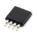
| 产品图片 |
|
| rohs | 符合RoHS无铅 / 符合限制有害物质指令(RoHS)规范要求 |
| 产品系列 | 数据转换器IC,数模转换器- DAC,Analog Devices AD5310BRMZ- |
| 数据手册 | |
| 产品型号 | AD5310BRMZ |
| 产品培训模块 | http://www.digikey.cn/PTM/IndividualPTM.page?site=cn&lang=zhs&ptm=19145http://www.digikey.cn/PTM/IndividualPTM.page?site=cn&lang=zhs&ptm=18614http://www.digikey.cn/PTM/IndividualPTM.page?site=cn&lang=zhs&ptm=26125http://www.digikey.cn/PTM/IndividualPTM.page?site=cn&lang=zhs&ptm=26140http://www.digikey.cn/PTM/IndividualPTM.page?site=cn&lang=zhs&ptm=26150http://www.digikey.cn/PTM/IndividualPTM.page?site=cn&lang=zhs&ptm=26147 |
| 产品目录页面 | |
| 产品种类 | 数模转换器- DAC |
| 位数 | 10 |
| 供应商器件封装 | 8-MSOP |
| 分辨率 | 10 bit |
| 包装 | 管件 |
| 商标 | Analog Devices |
| 安装类型 | 表面贴装 |
| 安装风格 | SMD/SMT |
| 封装 | Tube |
| 封装/外壳 | 8-TSSOP,8-MSOP(0.118",3.00mm 宽) |
| 封装/箱体 | MSOP-8 |
| 工作温度 | -40°C ~ 105°C |
| 工厂包装数量 | 50 |
| 建立时间 | 6µs |
| 接口类型 | SPI |
| 数据接口 | DSP,MICROWIRE™,QSPI™,串行,SPI™ |
| 最大功率耗散 | 1.25 mW |
| 最大工作温度 | + 105 C |
| 最小工作温度 | - 40 C |
| 标准包装 | 50 |
| 特色产品 | http://www.digikey.cn/product-highlights/zh/analog-devices-ad568x-and-ad569x-nanodac/52095http://www.digikey.cn/product-highlights/cn/zh/analog-devices-select-q2-2014-products/4186 |
| 电压参考 | External |
| 电压源 | 单电源 |
| 电源电压-最大 | 5.5 V |
| 电源电压-最小 | 2.7 V |
| 积分非线性 | +/- 4 LSB |
| 稳定时间 | 6 us |
| 系列 | AD5310 |
| 结构 | Resistor String |
| 转换器数 | 1 |
| 转换器数量 | 1 |
| 输出数和类型 | 1 电压,单极1 电压,双极 |
| 输出类型 | Voltage |
| 采样比 | 167 kS/s |
| 采样率(每秒) | 167k |


- 商务部:美国ITC正式对集成电路等产品启动337调查
- 曝三星4nm工艺存在良率问题 高通将骁龙8 Gen1或转产台积电
- 太阳诱电将投资9.5亿元在常州建新厂生产MLCC 预计2023年完工
- 英特尔发布欧洲新工厂建设计划 深化IDM 2.0 战略
- 台积电先进制程称霸业界 有大客户加持明年业绩稳了
- 达到5530亿美元!SIA预计今年全球半导体销售额将创下新高
- 英特尔拟将自动驾驶子公司Mobileye上市 估值或超500亿美元
- 三星加码芯片和SET,合并消费电子和移动部门,撤换高东真等 CEO
- 三星电子宣布重大人事变动 还合并消费电子和移动部门
- 海关总署:前11个月进口集成电路产品价值2.52万亿元 增长14.8%


PDF Datasheet 数据手册内容提取
2.7 V to 5.5 V, 140 µA, Rail-to-Rail Voltage Output 10-Bit DAC in a SOT-23 Data Sheet AD5310 FEATURES FUNCTIONAL BLOCK DIAGRAM Single 10-bit DAC 6-lead SOT-23 and 8-lead µSOIC packages Micropower operation: 140 µA @ 5 V Power-down to 200 nA @ 5 V, 50 nA @ 3 V 2.7 V to 5.5 V power supply Guaranteed monotonic by design Reference derived from power supply Power-on reset to 0 V Three power-down functions Low power serial interface with Schmitt triggered inputs On-chip output buffer amplifier, rail-to-rail operation SYNC interrupt facility Qualified for automotive applications APPLICATIONS Figure 1. Portable battery-powered instruments Digital gain and offset adjustment Programmable voltage and current sources Programmable attenuators GENERAL DESCRIPTION The AD53101 is a single, 10-bit, buffered voltage output DAC The AD5310 is one of a family of pin-compatible DACs. The that operates from a single 2.7 V to 5.5 V supply, consuming AD5300 is the 8-bit version, and the AD5320 is the 12-bit version. 115 µA at 3 V. Its on-chip precision output amplifier allows The AD5300/AD5310/AD5320 are available in 6-lead SOT-23 rail-to-rail output swing. The AD5310 utilizes a versatile 3-wire packages and 8-lead µSOIC packages. serial interface that operates at clock rates of up to 30 MHz and PRODUCT HIGHLIGHTS is compatible with standard SPI™, QSPI™, MICROWIRE®, and 1. Available in 6-lead SOT-23 and 8-lead µSOIC packages. DSP interface standards. 2. Low power, single-supply operation. This part operates The reference for AD5310 is derived from the power supply inputs from a single 2.7 V to 5.5 V supply and typically consumes and, therefore, provides the widest dynamic output range. The 0.35 mW at 3 V and 0.7 mW at 5 V, making it ideal for part incorporates a power-on reset circuit that ensures that the battery-powered applications. DAC output powers up to 0 V and remains there until a valid 3. The on-chip output buffer amplifier allows the output of write takes place to the device. The part contains a power-down the DAC to swing rail-to-rail with a slew rate of 1 V/µs. feature, which reduces the current consumption of the device to 4. Reference derived from the power supply. 200 nA at 5 V and provides software-selectable output loads while 5. High speed serial interface with clock speeds of up to 30 MHz. in power-down mode. The part is put into power-down mode Designed for very low power consumption. The interface over the serial interface. only powers up during a write cycle. The low power consumption of this part in normal operation 6. Power-down capability. When powered down, the DAC makes it ideally suited for portable, battery-operated equipment. typically consumes 50 nA at 3 V and 200 nA at 5 V. The power consumption is 0.7 mW at 5 V, reducing to 1 µW in power-down mode. 1 Patent pending; protected by U.S. Patent No. 5684481. Rev. B Information furnished by Analog Devices is believed to be accurate and reliable. However, no responsibility is assumed by Analog Devices for its use, nor for any infringements of patents or other One Technology Way, P.O. Box 9106, Norwood, MA 02062-9106, U.S.A. rights of third parties that may result from its use. Specifications subject to change without notice. No license is granted by implication or otherwise under any patent or patent rights of Analog Devices. Tel: 781.329.4700 www.analog.com Trademarks and registered trademarks are the property of their respective owners. Fax: 781.461.3113 ©2012 Analog Devices, Inc. All rights reserved.
AD5310 Data Sheet TABLE OF CONTENTS Features .............................................................................................. 1 Output Amplifier ........................................................................ 11 Applications ....................................................................................... 1 Serial Interface ............................................................................ 11 Functional Block Diagram .............................................................. 1 Input Shift Register .................................................................... 11 General Description ......................................................................... 1 SYNC Interrupt .......................................................................... 12 Product Highlights ........................................................................... 1 Power-On Reset .......................................................................... 12 Revision History ............................................................................... 2 Power-Down Modes .................................................................. 12 Specifications ..................................................................................... 3 Microprocessor Interfacing ....................................................... 12 Timing Characteristics ................................................................ 4 Applications Information .............................................................. 14 Absolute Maximum Ratings ............................................................ 5 Using REF19x as a Power Supply for AD5310 ....................... 14 ESD Caution .................................................................................. 5 Bipolar Operation Using the AD5310 ..................................... 14 Pin Configurations and Function Descriptions ........................... 6 Using AD5310 with an Opto-Isolated Interface .................... 14 Typical Performance Characteristics ............................................. 7 Power Supply Bypassing and Grounding ................................ 15 Terminology .................................................................................... 10 Outline Dimensions ....................................................................... 16 Theory of Operation ...................................................................... 11 Ordering Guide .......................................................................... 16 D/A Section ................................................................................. 11 Automotive Products ................................................................. 16 Resistor String ............................................................................. 11 REVISION HISTORY 7/12—Rev. A to Rev. B Updated Format .................................................................. Universal Changes to Features .......................................................................... 1 Change to Figure 9 Caption ............................................................ 7 Changes to AD5310 to ADSP-2101 Interface Section and Figure 27............................................................................... 12 Updated Outline Dimensions ....................................................... 16 Changes to Ordering Guide .......................................................... 16 Added Automotive Products Section........................................... 16 5/99—Rev. 0 to Rev. A Rev. B | Page 2 of 16
Data Sheet AD5310 SPECIFICATIONS V = 2.7 V to 5.5 V; temperature range = −40°C to +105°C R = 2 kΩ to GND; C = 500 pF to GND; all specifications T to T unless DD L L MIN MAX otherwise noted Table 1. Parameter Min Typ Max Unit Test Conditions/Comments STATIC PERFORMANCE1 Resolution 10 Bits Relative Accuracy ±4 LSB See Figure 5 Differential Nonlinearity ±0.5 LSB Guaranteed monotonic by design (see Figure 6) Zero Code Error 5 40 mV All 0s loaded to DAC register (see Figure 9) Full-Scale Error −0.15 −1.25 % of FSR All 1s loaded to DAC register (see Figure 9) Gain Error ±1.25 % of FSR Zero Code Error Drift −20 µV/°C Gain Temperature Coefficient −5 ppm of FSR/°C OUTPUT CHARACTERISTICS2 Output Voltage Range 0 V V DD Output Voltage Settling Time 6 8 µs ¼ scale to ¾ scale change (100 hex to 300 hex) Slew Rate 1 V/µs R = 2 kΩ; 0 pF < C < 500 pF (see Figure 19) L L Capacitive Load Stability 470 pF R = ∞ L 1000 pF R = 2 kΩ L Digital-to-Analog Glitch Impulse 20 nV-s 1 LSB change around major carry (see Figure 22) Digital Feedthrough 0.5 nV-s DC Output Impedance 1 Ω Short-Circuit Current 50 mA V = 5 V DD 20 mA V = 3 V DD Power-Up Time 2.5 µs Coming out of power-down mode, V = 5 V DD 5 µs Coming out of power-down mode, V = 3 V DD LOGIC INPUTS2 Input Current ±1 µA V , Input Low Voltage 0.8 V V = 5 V INL DD V , Input Low Voltage 0.6 V V = 3 V INL DD V , Input High Voltage 2.4 V V = 5 V INH DD V , Input High Voltage 2.1 V V = 3 V INH DD Pin Capacitance 3 pF POWER REQUIREMENTS V 2.7 5.5 V DD I (Normal Mode) DAC active and excluding load current DD V = 4.5 V to 5.5 V 140 250 µA V = V and V = GND DD IH DD IL V = 2.7 V to 3.6 V 115 200 µA V = V and V = GND DD IH DD IL I (All Power-Down Modes) DD V = 4.5 V to 5.5 V 0.2 1 µA V = V and V = GND DD IH DD IL V = 2.7 V to 3.6 V 0.05 1 µA V = V and V = GND DD IH DD IL Power Efficiency I /I 93 % I = 2 mA, V = 5 V OUT DD LOAD DD 1 Linearity calculated using a reduced code range of 12 to 1011. Output unloaded. 2 Guaranteed by design and characterization; not production tested. Rev. B | Page 3 of 16
AD5310 Data Sheet TIMING CHARACTERISTICS V = 2.7 V to 5.5 V; all specifications T to T unless otherwise noted DD MIN MAX Table 2. Limit at T , T MIN MAX Parameter1, 2 V = 2.7 V to 3.6 V V = 3.6 V to 5.5 V Unit Test Conditions/Comments DD DD t 3 50 33 ns min SCLK cycle time 1 t 13 13 ns min SCLK high time 2 t 22.5 13 ns min SCLK low time 3 t4 0 0 ns min SYNC to SCLK rising edge setup time t 5 5 ns min Data setup time 5 t 4.5 4.5 ns min Data hold time 6 t7 0 0 ns min SCLK falling edge to SYNC rising edge t8 50 33 ns min Minimum SYNC high time 1 All input signals are specified with tr = tf = 5 ns (10% to 90% of VDD) and timed from a voltage level of (VIL + VIH)/2. 2 See Figure 2. 3 Maximum SCLK frequency is 30 MHz at VDD = 3.6 V to 5.5 V and 20 MHz at VDD = 2.7 V to 3.6 V. Figure 2. Serial Write Operation Rev. B | Page 4 of 16
Data Sheet AD5310 ABSOLUTE MAXIMUM RATINGS T = 25°C unless otherwise noted Stresses above those listed under Absolute Maximum Ratings A may cause permanent damage to the device. This is a stress Table 3. rating only; functional operation of the device at these or any Parameter Rating other conditions above those indicated in the operational V to GND −0.3 V to +7 V DD section of this specification is not implied. Exposure to absolute Digital Input Voltage to GND −0.3 V to V + 0.3 V DD maximum rating conditions for extended periods may affect V to GND −0.3 V to V + 0.3 V OUT DD device reliability. Operating Temperature Range Industrial (B Version) −40°C to +105°C ESD CAUTION Storage Temperature Range −65°C to +150°C Junction Temperature (T Max) +150°C J SOT-23 Package Power Dissipation (T max − T )/θ J A JA θ Thermal Impedance 240°C/W JA Lead Temperature, Soldering Vapor Phase (60 sec) 215°C Infrared (15 sec) 220°C µSOIC Package Power Dissipation (T max − T )/θ J A JA θ Thermal Impedance 206°C/W JA θ Thermal Impedance 44°C/W JC Lead Temperature, Soldering Vapor Phase (60 sec) 215°C Infrared (15 sec) 220°C Rev. B | Page 5 of 16
AD5310 Data Sheet PIN CONFIGURATIONS AND FUNCTION DESCRIPTIONS Figure 3. SOT-23 Figure 4. µSOIC Table 4. SOT-23 Pin Function Descriptions Pin No. Mnemonic Description 1 V Analog Output Voltage from DAC. The output amplifier has rail-to-rail operation. OUT 2 GND Ground Reference Point for All Circuitry on the Part. 3 V Power Supply Input. These parts can be operated from 2.5 V to 5.5 V, and V should be decoupled to GND. DD DD 4 DIN Serial Data Input. This device has a 16-bit shift register. Data is clocked into the register on the falling edge of the serial clock input. 5 SCLK Serial Clock Input. Data is clocked into the input shift register on the falling edge of the serial clock input. Data can be transferred at rates of up to 30 MHz. 6 SYNC Level Triggered Control Input (Active Low). This is the frame synchronization signal for the input data. When SYNC goes low, it enables the input shift register, and data is transferred in on the falling edges of the following clocks. The DAC is updated following the 16th clock cycle unless SYNC is taken high before this edge, in which case the rising edge of SYNC acts as an interrupt and the write sequence is ignored by the DAC. Rev. B | Page 6 of 16
Data Sheet AD5310 TYPICAL PERFORMANCE CHARACTERISTICS Figure 5. Typical INL Figure 8. INL Error and DNL Error vs. Temperature Figure 6. Typical DNL Figure 9. Zero Code Error and Full-Scale Error vs. Temperature Figure 7. Typical Total Unadjusted Error Figure 10. IDD Histogram with VDD = 3 V and VDD = 5 V Rev. B | Page 7 of 16
AD5310 Data Sheet Figure 11. Source and Sink Current Capability with VDD = 3 V Figure 14. Supply Current vs. Temperature Figure 12. Source and Sink Current Capability with VDD = 5 V Figure 15. Supply Current vs. Supply Voltage Figure 13. Supply Current vs. Code Figure 16. Power-Down Current vs. Supply Voltage Rev. B | Page 8 of 16
Data Sheet AD5310 Figure 17. Supply Current vs. Logic Input Voltage Figure 20. Power-On Reset to 0 V Figure 18. Full-Scale Settling Time Figure 21. Exiting Power-Down (200 Hex Loaded) Figure 19. Half-Scale Settling Time Figure 22. Digital-to-Analog Glitch Impulse Rev. B | Page 9 of 16
AD5310 Data Sheet TERMINOLOGY Gain Error Relative Accuracy Gain error is a measure of the span error of the DAC. It is the For the DAC, relative accuracy or integral nonlinearity (INL) is deviation in slope of the DAC transfer characteristic from the a measure of the maximum deviation, in LSBs, from a straight ideal expressed as a percentage of the full-scale range. line passing through the endpoints of the DAC transfer function. A typical INL vs. code plot is shown in Figure 5. Total Unadjusted Error Total unadjusted error (TUE) is a measure of the output error Differential Nonlinearity that takes all the various errors into account. A typical TUE vs. Differential nonlinearity (DNL) is the difference between the code plot is shown in Figure 7. measured change and the ideal 1 LSB change between any two adjacent codes. A specified differential nonlinearity of ±1 LSB Zero Code Error Drift maximum ensures monotonicity. This DAC is guaranteed mono- Zero code error drift is a measure of the change in zero code tonic by design. A typical DNL vs. code plot is shown in Figure 6. error with a change in temperature. It is expressed in µV/°C. Zero Code Error Gain Error Drift Zero code error is a measure of the output error when zero code Gain error drift is a measure of the change in gain error with (000 hex) is loaded to the DAC register. Ideally, the output should changes in temperature. It is expressed in (ppm of full-scale be 0 V. The zero code error is always positive in the AD5310 range)/°C. because the output of the DAC cannot go below 0 V. It is due to Digital-to-Analog Glitch Impulse a combination of the offset errors in the DAC and output amplifier. Digital-to-analog glitch impulse is the impulse injected into the Zero code error is expressed in mV. A plot of zero code error vs. analog output when the input code in the DAC register changes temperature is shown in Figure 9. state. It is normally specified as the area of the glitch in nV-s and Full-Scale Error is measured when the digital input code is changed by 1 LSB at Full-scale error is a measure of the output error when full-scale the major carry transition (1FF hex to 200 hex). See Figure 22. code (3FF Hex) is loaded to the DAC register. Ideally, the output Digital Feedthrough should be V − 1 LSB. Full-scale error is expressed as a percentage DD Digital feedthrough is a measure of the impulse injected into the of the full-scale range. A plot of full-scale error vs. temperature analog output of the DAC from the digital inputs of the DAC is shown in Figure 9. but is measured when the DAC output is not updated. It is specified in nV-s and is measured with a full-scale code change on the data bus, that is, from all 0s to all 1s and vice versa. Rev. B | Page 10 of 16
Data Sheet AD5310 THEORY OF OPERATION D/A SECTION to the amplifier. Because it is a string of resistors, it is guaranteed monotonic. The AD5310 DAC is fabricated on a CMOS process. The architecture consists of a string DAC followed by an output OUTPUT AMPLIFIER buffer amplifier. Because there is no reference input pin, the The output buffer amplifier is capable of generating rail-to-rail power supply (V ) acts as the reference. Figure 23 shows a DD voltages on its output, which results in an output range of 0 V to block diagram of the DAC architecture. V . It is capable of driving a load of 2 kΩ in parallel with 1000 pF DD to GND. The source and sink capabilities of the output amplifier can be seen in Figure 11 and Figure 12. The slew rate is 1 V/µs with a half-scale settling time of 6 µs with the output loaded. SERIAL INTERFACE The AD5310 has a 3-wire serial interface (SYNC, SCLK, and DIN) that is compatible with SPI, QSPI, and MICROWIRE Figure 23. DAC Architecture interface standards, as well as most DSPs. See Figure 2 for a Because the input coding to the DAC is straight binary, the ideal timing diagram of a typical write sequence. output voltage is given by The write sequence begins by bringing the SYNC line low. Data D from the DIN line is clocked into the 16-bit shift register on the V =V × OUT DD 1024 falling edge of SCLK. The serial clock frequency can be as high as 30 MHz, making the AD5310 compatible with high speed where D is the decimal equivalent of the binary code that is DSPs. On the 16th falling clock edge, the last data bit is clocked loaded to the DAC register; it can range from 0 to 1023. in and the programmed function is executed (that is, a change in DAC register contents and/or a change in the mode of operation). At this stage, the SYNC line can be kept low or be brought high. In either case, it must be brought high for a minimum of 33 ns before the next write sequence so that a falling edge of SYNC can initiate the next write sequence. Because the SYNC buffer draws more current when V = 2.4 V than it does when V = IN IN 0.8 V, SYNC should be idled low between write sequences for even lower power operation of the part. As previously mentioned, however, it must be brought high again just before the next write sequence. INPUT SHIFT REGISTER The input shift register is 16 bits wide (see Figure 25). The first two bits are don’t cares. The next two bits are control bits that Figure 24. Resistor String control which mode of operation the part is in (normal mode or RESISTOR STRING one of the three power-down modes). There is a more complete description of the various modes in the Power-Down Modes The resistor string section is shown in Figure 24. It is simply a section. The next 10 bits are the data bits. These are transferred string of resistors, each of value R. The code loaded to the DAC to the DAC register on the 16th falling edge of SCLK. Finally, register determines at what node on the string the voltage is the last two bits are don’t cares. tapped off to be fed into the output amplifier. The voltage is tapped off by closing one of the switches connecting the string Figure 25. Input Register Contents Rev. B | Page 11 of 16
AD5310 Data Sheet SYNC INTERRUPT the part is in power-down mode. There are three options. The output is connected internally to GND through a 1 kΩ resistor, In a normal write sequence, the SYNC line is kept low for at a 100 kΩ resistor, or it is left open-circuited (three-state). The least 16 falling edges of SCLK, and the DAC is updated on the output stage is illustrated in Figure 26. 16th falling edge. However, if SYNC is brought high before the 16th falling edge, this acts as an interrupt to the write sequence. The shift register is reset, and the write sequence is seen as invalid. Neither an update of the DAC register contents or a change in the operating mode occurs (see Figure 28). POWER-ON RESET The AD5310 contains a power-on reset circuit that controls the output voltage during power-up. The DAC register is filled with Figure 26. Output Stage During Power-Down 0s, and the output voltage is 0 V. It remains there until a valid write sequence is performed to the DAC. This is useful in The bias generator, the output amplifier, the resistor string, and applications where it is important to know the state of the other associated linear circuitry are all shut down when the output of the DAC while it is in the process of powering up. power-down mode is activated. However, the contents of the DAC register are unaffected when in power-down. The time to POWER-DOWN MODES exit power-down is typically 2.5 µs for V = 5 V and 5 µs for DD The AD5310 contains four separate modes of operation. These V = 3 V (see Figure 21). DD modes are software programmable by setting two bits (DB13 MICROPROCESSOR INTERFACING and DB12) in the control register. Table 5 shows how the state AD5310 to ADSP-2101 Interface of the bits corresponds to the mode of operation of the device. Figure 27 shows a serial interface between the AD5310 and the Table 5. Modes of Operation for the AD5310 ADSP-2101. The ADSP-2101 should be set up to operate in the Operating Mode DB13 DB12 SPORT transmit alternate framing mode. The ADSP-2101SPORT Normal Operation 0 0 is programmed through the SPORT control register and should Power-Down Modes be configured as follows: internal clock operation, active low 1 kΩ to GND 0 1 framing, 16-bit word length. Transmission is initiated by writing 100 kΩ to GND 1 0 a word to the Tx register after the SPORT has been enabled. Three-State 1 1 ADSP-2101* AD5310* When both bits are set to 0, the part works normally with its TFS SYNC normal power consumption of 140 µA at 5 V. However, for the DT DIN three power-down modes, the supply current falls to 200 nA at SCLK SCLK 5 V (50 nA at 3 V). Not only does the supply current fall, but the output stage is also internally switched from the output of *ADDITIONAL PINS OMITTED FOR CLARITY Figure 27. AD5310 to ADSP-2101 Interface the amplifier to a resistor network of known values. This has the advantage of knowing the output impedance of the part when Figure 28. SYNC Interrupt Facility Rev. B | Page 12 of 16
Data Sheet AD5310 AD5310 to 68HC11/68L11 Interface transmitted to the AD5310, P3.3 is taken low. The 80C51/80L51 transmits data only in 8-bit bytes; therefore, only eight falling Figure 29 shows a serial interface between the AD5310 and the clock edges occur in the transmit cycle. To load data to the 68HC11/68L11 microcontroller. SCK of the 68HC11/68L11 DAC, P3.3 is left low after the first eight bits are transmitted, drives the SCLK of the AD5310, while the MOSI output drives and a second write cycle is initiated to transmit the second byte the serial data line of the DAC. The SYNC signal is derived of data. P3.3 is taken high following the completion of this from a port line (PC7). The setup conditions for correct cycle. The 80C51/ 80L51 outputs the serial data in a format that operation of this interface are as follows: the 68HC11/68L11 has the LSB first. The AD5310 requires that the MSB of data be should be configured so that its CPOL bit is a 0 and its CPHA received first. The 80C51/80L51 transmit routine should take bit is a 1. When data is being transmitted to the DAC, the SYNC this into account. line is taken low (PC7). With this 68HC11/68L11 configuration, data appearing on the MOSI output is valid on the falling edge of SCK. Serial data from the 68HC11/68L11 is transmitted in 8-bit bytes with only eight falling clock edges occurring in the transmit cycle. Data is transmitted MSB first. To load data to the AD5310, PC7 is left low after the first eight bits are transferred, a second serial write operation is performed to the DAC, and PC7 is taken high at the end of this procedure. Figure 30. AD5310 to 80C51/80L51 Interface AD5310 to MICROWIRE Interface Figure 31 shows an interface between the AD5310 and any MICROWIRE-compatible device. Serial data is shifted out on the falling edge of the serial clock and is clocked into the AD5310 on the rising edge of the SK. Figure 29. AD5310 to 68HC11/68L11 Interface AD5310 to 80C51/80L51 Interface Figure 30 shows a serial interface between the AD5310 and the 80C51/80L51 microcontroller. The setup for the interface is as follows: TXD of the 80C51/80L51 drives SCLK of the AD5310 Figure 31. AD5310 to MICROWIRE Interface while RXD drives the serial data line of the part. The SYNC signal is again derived from a bit-programmable pin on the port. In this case, Port Line P3.3 is used. When data is to be Rev. B | Page 13 of 16
AD5310 Data Sheet APPLICATIONS INFORMATION USING REF19x AS A POWER SUPPLY FOR AD5310 Because the supply current required by the AD5310 is extremely low, an alternative option is to use a REF19x voltage reference (REF195 for 5 V or REF193 for 3 V) to supply the required voltage to the part (see Figure 32). This is especially useful if the power supply is quite noisy or if the system supply voltages are at some value other than 5 V or 3 V (for example, 15 V). The REF19x outputs a steady supply voltage for the AD5310. If the low dropout REF195 is used, the current that it needs to supply to the AD5310 is 140 µA. This is with no load on the output of the DAC. When the DAC output is loaded, the REF195 also needs to supply the Figure 33. Bipolar Operation with the AD5310 current to the load. The total current required (with a 5 kΩ load USING AD5310 WITH AN OPTO-ISOLATED on the DAC output) is INTERFACE 140 µA + (5 V/5 kΩ) = 1.14 mA In process control applications in industrial environments, it is The load regulation of the REF195 is typically 2 ppm/mA, which often necessary to use an opto-isolated interface to protect and results in an error of 2.3 ppm (11.5 µV) for the 1.14 mA current isolate the controlling circuitry from any hazardous common- drawn from it. This corresponds to a 0.002 LSB error. mode voltages that may occur in the area where the DAC is functioning. Opto-isolators provide isolation in excess of 3 kV. Because the AD5310 uses a 3-wire serial logic interface, it only requires three opto-isolators to provide the required isolation (see Figure 34). The power supply to the part also needs to be isolated. This is done by using a transformer. On the DAC side of the transformer, a 5 V regulator provides the 5 V supply required for the AD5310. Figure 32. REF195 as Power Supply to AD5310 BIPOLAR OPERATION USING THE AD5310 The AD5310 is designed for single-supply operation but a bipolar output range is also possible using the circuit shown in Figure 33. This circuit results in an output voltage range of ±5 V. Rail-to-rail operation at the amplifier output is achievable using an AD820 or an OP295 as the output amplifier. The output voltage for any input code can be calculated as follows: D R1+R2 R2 VO =VDD×1024× R1 −VDD×R1 where D represents the input code in decimal (0 to 1023). With VDD = 5 V, R1 = R2 = 10 kΩ, Figure 34. AD5310 with an Opto-Isolated Interface 10×D V = −5V O 1024 This is an output voltage range of ±5 V, with 000 hex corresponding to a −5 V output and 3FF hex corresponding to a +5 V output. Rev. B | Page 14 of 16
Data Sheet AD5310 POWER SUPPLY BYPASSING AND GROUNDING 0.1 µF capacitor provides a low impedance path to ground for high frequencies caused by transient currents due to internal When accuracy is important in a circuit, it is helpful to carefully logic switching. consider the power supply and ground return layout on the board. The printed circuit board containing the AD5310 should have The power supply line itself should have as large a trace as possible separate analog and digital sections, each having their own area to provide a low impedance path and to reduce glitch effects on of the board. If the AD5310 is in a system where other devices the supply line. Clocks and other fast switching digital signals require an AGND to DGND connection, the connection should should be shielded from other parts of the board by digital be made at one point only. This ground point should be as close ground. Avoid crossover of digital and analog signals if possible. as possible to the AD5310. When traces cross on opposite sides of the board, ensure that they run at right angles to each other to reduce feedthrough effects The power supply to the AD5310 should be bypassed with 10 µF through the board. The best board layout technique is the micro- and 0.1 µF capacitors. The capacitors should be physically as strip technique, where the component side of the board is close as possible to the device, with the 0.1 µF capacitor ideally dedicated to the ground plane only and the signal traces are right up against the device. The 10 µF capacitors are the tantalum placed on the solder side. However, this is not always possible bead type. It is important that the 0.1 µF capacitor has low effective with a 2-layer board. series resistance (ESR) and effective series inductance (ESI), such as is the case with common ceramic types of capacitors. This Rev. B | Page 15 of 16
AD5310 Data Sheet OUTLINE DIMENSIONS 3.00 3.20 2.90 3.00 2.80 2.80 1.70 6 5 4 3.00 8 5 5.15 1.60 2.80 3.20 4.90 1.50 1 2 3 2.60 3.00 4.65 2.80 1 4 PIN1 INDICATOR 0.95BSC PIN1 1.90 IDENTIFIER BSC 0.65BSC 1.30 1.15 0.90 0.95 15°MAX 1.45MAX 0.20MAX 0.85 1.10MAX 0.95MIN 0.08MIN 0.75 00..1055MMAINX COMPLIA00N..53T00TMMOAINXJEDECSPSELTAAATNNIENDGARDSMO-178-A140B0°°° B0S.6C0 000...543555 12-16-2008-A CO00P..10L550A.1N0ARICTOYMPLIANT00..T4205OJEDECSTA60°°NDARDS00M..20O39-187-AA 000...854050 10-07-2009-B Figure 35. 6-Lead Small Outline Transistor Package [SOT-23] Figure 36. 8-Lead Mini Small Outline Package [MSOP] (RJ-6) (RM-8) Dimensions shown in millimeters Dimensions shown in millimeters ORDERING GUIDE Model1, 2 Temperature Range Package Description Package Option Branding Information AD5310BRTZ-REEL –40°C to +105°C 6-Lead SOT-23 RJ-6 D3B AD5310BRTZ-REEL7 –40°C to +105°C 6-Lead SOT-23 RJ-6 D3B AD5310BRTZ-500RL7 –40°C to +105°C 6-Lead SOT-23 RJ-6 D3B AD5310BRT-REEL –40°C to +105°C 6-Lead SOT-23 RJ-6 D3B AD5310BRT-REEL7 –40°C to +105°C 6-Lead SOT-23 RJ-6 D3B AD5310BRT-500RL7 –40°C to +105°C 6-Lead SOT-23 RJ-6 D3B AD5310WBRTZ-REEL7 –40°C to +105°C 6-Lead SOT-23 RJ-6 DJW AD5310BRMZ –40°C to +105°C 8-Lead MSOP RM-8 D3B AD5310BRMZ-REEL7 –40°C to +105°C 8-Lead MSOP RM-8 D3B AD5310BRM –40°C to +105°C 8-Lead MSOP RM-8 D3B AD5310BRM-REEL –40°C to +105°C 8-Lead MSOP RM-8 D3B 1 Z = RoHS Compliant Part. 2 W = Qualified for Automotive Applications. AUTOMOTIVE PRODUCTS The AD5310WBRTZ-REEL7 model is available with controlled manufacturing to support the quality and reliability requirements of automotive applications. Note that this automotive model may have specifications that differ from the commercial models; therefore, designers should review the Specifications section of this data sheet carefully. Only the automotive grade product shown is available for use in automotive applications. Contact your local Analog Devices account representative for specific product ordering information and to obtain the specific Automotive Reliability reports for this model. ©2012 Analog Devices, Inc. All rights reserved. Trademarks and registered trademarks are the property of their respective owners. D00933-0-7/12(B) Rev. B | Page 16 of 16
Mouser Electronics Authorized Distributor Click to View Pricing, Inventory, Delivery & Lifecycle Information: A nalog Devices Inc.: AD5310BRT-REEL AD5310BRTZ-REEL7 AD5310BRM AD5310BRTZ-REEL AD5310BRTZ-500RL7 AD5310BRT- REEL7 AD5310BRMZ AD5310BRM-REEL AD5310BRMZ-REEL7 AD5310BRT-500RL7