ICGOO在线商城 > 集成电路(IC) > 数据采集 - 数模转换器 > AD5791ARUZ
 Datasheet下载
- 型号: AD5791ARUZ
- 制造商: Analog
- 库位|库存: xxxx|xxxx
- 要求:
| 数量阶梯 | 香港交货 | 国内含税 |
| +xxxx | $xxxx | ¥xxxx |
查看当月历史价格
查看今年历史价格
AD5791ARUZ产品简介:
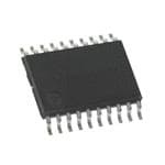
ICGOO电子元器件商城为您提供AD5791ARUZ由Analog设计生产,在icgoo商城现货销售,并且可以通过原厂、代理商等渠道进行代购。 AD5791ARUZ价格参考。AnalogAD5791ARUZ封装/规格:数据采集 - 数模转换器, 20 Bit Digital to Analog Converter 1 20-TSSOP。您可以下载AD5791ARUZ参考资料、Datasheet数据手册功能说明书,资料中有AD5791ARUZ 详细功能的应用电路图电压和使用方法及教程。
AD5791ARUZ是Analog Devices Inc.推出的一款高精度、18位数模转换器(DAC),属于数据采集-数模转换器类别。该器件具有极低的积分非线性(INL)和差分非线性(DNL),确保了出色的静态精度,适用于对精度要求极高的应用场景。

AD5791ARUZ广泛应用于精密测试与测量设备,如数字万用表、自动测试设备(ATE)和校准系统,能够提供稳定可靠的模拟输出信号。在工业控制系统中,它可用于高精度过程控制、阀门调节和传感器激励,确保控制信号的准确性和稳定性。此外,该DAC也适用于医疗仪器,如病人监护设备和成像系统,满足其对信号精度和可靠性的严苛要求。

由于具备低噪声、低温漂和宽电源电压范围等特性,AD5791ARUZ还适合用于精密电源控制、光通信系统中的偏置调节以及航空航天与国防领域的高可靠性系统。其串行接口设计便于与微控制器或FPGA连接,提升了系统集成的灵活性。

总之,AD5791ARUZ凭借其高分辨率和卓越的直流精度,成为需要超高精度模拟输出的关键应用中的理想选择。
| 参数 | 数值 |
| 产品目录 | 集成电路 (IC)半导体 |
| 描述 | IC DAC 20BIT SRL 20TSSOP数模转换器- DAC 1ppm 20B+/-1 LSB INL VOut |
| DevelopmentKit | EVAL-AD5791SDZ |
| 产品分类 | |
| 品牌 | Analog Devices Inc |
| 产品手册 | |
| 产品图片 |
|
| rohs | 符合RoHS无铅 / 符合限制有害物质指令(RoHS)规范要求 |
| 产品系列 | 数据转换器IC,数模转换器- DAC,Analog Devices AD5791ARUZ- |
| 数据手册 | |
| 产品型号 | AD5791ARUZ |
| PCN设计/规格 | |
| 产品培训模块 | http://www.digikey.cn/PTM/IndividualPTM.page?site=cn&lang=zhs&ptm=26125http://www.digikey.cn/PTM/IndividualPTM.page?site=cn&lang=zhs&ptm=26140http://www.digikey.cn/PTM/IndividualPTM.page?site=cn&lang=zhs&ptm=26150http://www.digikey.cn/PTM/IndividualPTM.page?site=cn&lang=zhs&ptm=26147 |
| 产品种类 | 数模转换器- DAC |
| 位数 | 20 |
| 供应商器件封装 | 20-TSSOP |
| 分辨率 | 20 bit |
| 包装 | 管件 |
| 商标 | Analog Devices |
| 安装类型 | 表面贴装 |
| 安装风格 | SMD/SMT |
| 封装 | Tube |
| 封装/外壳 | 20-TSSOP(0.173",4.40mm 宽) |
| 封装/箱体 | TSSOP-20 |
| 工作温度 | -40°C ~ 125°C |
| 工厂包装数量 | 75 |
| 建立时间 | 1µs |
| 接口类型 | SPI |
| 数据接口 | DSP,MICROWIRE™,QSPI™,串行,SPI™ |
| 最大功率耗散 | 126.3 mW |
| 最大工作温度 | + 125 C |
| 最小工作温度 | - 40 C |
| 标准包装 | 1 |
| 电压参考 | External |
| 电压源 | 模拟和数字,双 ± |
| 电源电压-最大 | 5.5 V |
| 电源电压-最小 | 2.7 V |
| 积分非线性 | +/- 4 LSB |
| 稳定时间 | 1 us |
| 系列 | AD5791 |
| 结构 | R-2R |
| 转换器数 | 1 |
| 转换器数量 | 1 |
| 输出数和类型 | 1 电压,双极 |
| 输出类型 | Voltage |
| 采样比 | 1 MSPs |
| 采样率(每秒) | - |


.jpg)


- 商务部:美国ITC正式对集成电路等产品启动337调查
- 曝三星4nm工艺存在良率问题 高通将骁龙8 Gen1或转产台积电
- 太阳诱电将投资9.5亿元在常州建新厂生产MLCC 预计2023年完工
- 英特尔发布欧洲新工厂建设计划 深化IDM 2.0 战略
- 台积电先进制程称霸业界 有大客户加持明年业绩稳了
- 达到5530亿美元!SIA预计今年全球半导体销售额将创下新高
- 英特尔拟将自动驾驶子公司Mobileye上市 估值或超500亿美元
- 三星加码芯片和SET,合并消费电子和移动部门,撤换高东真等 CEO
- 三星电子宣布重大人事变动 还合并消费电子和移动部门
- 海关总署:前11个月进口集成电路产品价值2.52万亿元 增长14.8%


PDF Datasheet 数据手册内容提取
1 ppm, 20-Bit, ±1 LSB INL, Voltage Output DAC Enhanced Product AD5791-EP FEATURES FUNCTIONAL BLOCK DIAGRAM 1 ppm resolution VCC VDD VREFPF VREFPS 1 ppm INL 7.5 nV/√Hz noise spectral density IOVCC AD5791-EP A1 6.8kΩ 6.8kΩ RFB 0.19 LSB long-term linearity stability R1 RFB INV 1< 0µ.s0 5se pttplmin/g° Cti mteem perature drift SSSYCDNLICNK REISNGAHPINSIUFDTTTER 20 RDEAGC 20 2D0-ABCIT VOUT CONTROL 1.4 nV-sec glitch impulse SDO LOGIC 20-lead TSSOP package 6kΩ LDAC Wide power supply range up to ±16.5 V 35 MHz Schmitt triggered digital interface CLR POWER-ON RESET RESET AND CLEAR LOGIC 1.8 V compatible digital interface ENHANCED PRODUCT FEATURES DGND VSS AGND VREFNFVREFNS 10455-001 Figure 1. Supports defense and aerospace applications (AQEC COMPANION PRODUCTS standard) Military temperature range (−55°C to +125°C) Ultra precision op amps: AD8675, AD8676 Controlled manufacturing baseline High voltage op amp: ADA4898-1 One assembly/test site Additional companion products on the AD5791 product page One fabrication site Product change notification Table 1. Related Device Qualification data available on request Part No. Description AD5781 18-bit, 0.5 LSB INL, voltage output DAC APPLICATIONS Medical instrumentation Test and measurement Industrial control High end scientific and aerospace instrumentation GENERAL DESCRIPTION The AD5791-EP1 is a single 20-bit, unbuffered voltage-output valid write to the device takes place. The part provides an digital-to-analog converter (DAC) that operates from a bipolar output clamp feature that places the output in a defined load supply of up to 33 V. The AD5791 accepts a positive reference state. input in the range 5 V to V − 2.5 V and a negative reference DD The AD5791-EP is available in a compact, 20-lead TSSOP input in the range V + 2.5 V to 0 V. The AD5791-EP offers a SS package and operates at the extended automotive temperature relative accuracy specification of ±1 LSB max, and operation is range of −55°C to +125°C. Additional application and technical guaranteed monotonic with a ±1 LSB differential nonlinearity information can be found in the AD5791 data sheet. (DNL) maximum specification. PRODUCT HIGHLIGHTS The part uses a versatile 3-wire serial interface that operates at 1. 1 ppm Accuracy. clock rates up to 35 MHz and that is compatible with standard 2. Wide Power Supply Range up to ±16.5 V. serial peripheral interface (SPI), QSPI™, MICROWIRE™, and 3. Operating Temperature Range: −55°C to +125°C. DSP interface standards. The part incorporates a power-on 4. Low 7.5 nV/√Hz Noise Spectral Density. reset circuit that ensures the DAC output powers up to 0 V in a 5. Low 0.05 ppm/°C Temperature Drift. known output impedance state and remains in this state until a 1 Protected by U.S. Patents No. 7,884,747 and 8,089,380. Other patents pending. Rev. B Document Feedback Information furnished by Analog Devices is believed to be accurate and reliable. However, no responsibility is assumed by Analog Devices for its use, nor for any infringements of patents or other One Technology Way, P.O. Box 9106, Norwood, MA 02062-9106, U.S.A. rights of third parties that may result from its use. Specifications subject to change without notice. No license is granted by implication or otherwise under any patent or patent rights of Analog Devices. Tel: 781.329.4700 ©2012–2018 Analog Devices, Inc. All rights reserved. Trademarks and registered trademarks are the property of their respective owners. Technical Support www.analog.com
AD5791-EP Enhanced Product TABLE OF CONTENTS Features .............................................................................................. 1 Specifications .....................................................................................3 Enhanced Product Features ............................................................ 1 Timing Characteristics .................................................................5 Applications ....................................................................................... 1 Absolute Maximum Ratings ............................................................7 Functional Block Diagram .............................................................. 1 ESD Caution...................................................................................7 Companion Products ....................................................................... 1 Pin Configuration and Function Descriptions ..............................8 General Description ......................................................................... 1 Typical Performance Characteristics ..............................................9 Product Highlights ........................................................................... 1 Outline Dimensions ....................................................................... 17 Revision History ............................................................................... 2 Ordering Guide .......................................................................... 17 REVISION HISTORY 3/2018—Rev. A to Rev. B Changes to Features Section and Enhanced Product Features Section ................................................................................................ 1 Changes to Ordering Guide .......................................................... 17 7/2013—Rev. 0 to Rev. A Changes to t Test Conditions/Comments and Endnote 2 ......... 5 1 Deleted Figure 4 ................................................................................ 7 2/2012—Revision 0: Initial Version Rev. B | Page 2 of 17
Enhanced Product AD5791-EP SPECIFICATIONS V = 12.5 V to 16.5 V, V = −16.5 V to −12.5 V, V = 10 V, V = −10 V, V = 2.7 V to +5.5 V, IOV = 1.71 V to 5.5 V, DD SS REFP REFN CC CC R = unloaded, C = unloaded, all specifications T to T , unless otherwise noted. L L MIN MAX Table 2. Parameter1 Min Typ Max Unit Test Conditions/Comments STATIC PERFORMANCE2 Resolution 20 Bits Integral Nonlinearity Error (Relative Accuracy) −1 ±0.25 +1 LSB V = +10 V, V = −10 V, REFP REFN T = 0°C to 105°C A −1.5 ±0.25 +1.5 LSB V = +10 V, V = −10 V REFP REFN −1.5 ±0.5 +1.5 LSB V = 10 V, V = 0 V3 REFP REFN −3 ±1 +3 LSB V = 5 V, V = 0 V3 REFP REFN Differential Nonlinearity Error −1 ±0.5 +1 LSB V = +10 V, V = −10 V REFP REFN −1.5 ±0.75 +1.5 LSB V = 10 V, V = 0 V REFP REFN −2.5 ±1 +2.5 LSB V = 5 V, V = 0 V REFP REFN Linearity Error Long-Term Stability4 0.16 LSB After 500 hours at T = 125°C A 0.19 LSB After 1000 hours at T = 125°C A 0.11 LSB After 1000 hours at T = 100°C A Full-Scale Error −7 ±0.1 +7 LSB V = +10 V, V = −10 V3 REFP REFN −11 ±0.25 +11 LSB V = 10 V, V = 0 V3 REFP REFN −21 ±0.8 +21 LSB V = 5 V, V = 0 V3 REFP REFN −4 ±0.1 +4 LSB V = +10 V, V = −10 V3, T = 0°C to 105°C REFP REFN A −4 ±0.25 +4 LSB V = 10 V, V = 0 V3, T = 0°C to 105°C REFP REFN A −6 ±0.8 +6 LSB V = 5 V, V = 0 V3, T = 0°C to 105°C REFP REFN A Full-Scale Error Temperature Coefficient ±0.02 ppm FSR/°C Zero-Scale Error −7 ±0.1 +7 LSB V = +10 V, V = −10 V3 REFP REFN −10 ±0.15 +10 LSB V = 10 V, V = 0 V3 REFP REFN −21 ±0.75 +21 LSB V = 5 V, V = 0 V3 REFP REFN −4 ±0.1 +4 LSB V = +10 V, V = −10 V3, T = 0°C to 105°C REFP REFN A −4 ±0.15 +4 LSB V = 10 V, V = 0 V3, T = 0°C to 105°C REFP REFN A −6 ±0.75 +6 LSB V = 5 V, V = 0 V3, T = 0°C to 105°C REFP REFN A Zero-Scale Error Temperature Coefficient3 ±0.04 ppm FSR/°C Gain Error −6 ±0.3 +6 ppm FSR V = +10 V, V = −10 V3 REFP REFN −10 ±0.4 +10 ppm FSR V = 10 V, V = 0 V3 REFP REFN −20 ±0.4 +20 ppm FSR V = 5 V, V = 0 V3 REFP REFN −6 ±0.3 +6 ppm FSR V = +10 V, V = −10 V3, T = 0°C to 105°C REFP REFN A −6 ±0.4 +6 ppm FSR V = 10 V, V = 0 V3, T = 0°C to 105°C REFP REFN A −7 ±0.4 +7 ppm FSR V = 5 V, V = 0 V3, T = 0°C to 105°C REFP REFN A Gain Error Temperature Coefficient3 ±0.04 ppm FSR/°C R1, R Matching 0.01 % FB OUTPUT CHARACTERISTICS3 Output Voltage Range V V V REFN REFP Output Slew Rate 50 V/µs Output Voltage Settling Time 1 µs 10 V step to 0.02%, using the AD845 buffer in unity-gain mode 1 µs 500 code step to ±1 LSB5 Output Noise Spectral Density 7.5 nV/√Hz at 1 kHz, DAC code = midscale 7.5 nV/√Hz at 10 kHz, DAC code = midscale 7.5 nV/√Hz At 100 kHz, DAC code = midscale Output Voltage Noise 1.1 µV p-p DAC code = midscale, 0.1 Hz to 10 Hz bandwidth6 Rev. B | Page 3 of 17
AD5791-EP Enhanced Product Parameter1 Min Typ Max Unit Test Conditions/Comments Midscale Glitch Impulse7 3.1 nV-sec V = +10 V, V = −10 V REFP REFN 1.7 nV-sec V = 10 V, V = 0 V REFP REFN 1.4 nV-sec V = 5 V, V = 0 V REFP REFN MSB Segment Glitch Impulse7 9.1 nV-sec V = +10 V, V = −10 V, see Figure 42 REFP REFN 3.6 nV-sec V = 10 V, V = 0 V, see Figure 43 REFP REFN 1.9 nV-sec V = 5 V, V = 0 V, see Figure 44 REFP REFN Output Enabled Glitch Impulse 45 nV-sec On removal of output ground clamp Digital Feedthrough 0.4 nV-sec DC Output Impedance (Normal Mode) 3.4 kΩ DC Output Impedance (Output Clamped 6 kΩ to Ground) Spurious Free Dynamic Range 100 dB 1 kHz tone, 10 kHz sample rate Total Harmonic Distortion 97 dB 1 kHz tone, 10 kHz sample rate REFERENCE INPUTS3 V Input Range 5 V − 2.5 V V REFP DD V Input Range V + 2.5 V 0 REFN SS DC Input Impedance 5 6.6 kΩ V , V , code dependent, REFP REFN typical at midscale code Input Capacitance 15 pF V , V REFP REFN LOGIC INPUTS3 Input Current8 −1 +1 µA Input Low Voltage, V 0.3 × IOV V IOV = 1.71 V to 5.5 V IL CC CC Input High Voltage, V 0.7 × IOV V IOV = 1.71 V to 5.5 V IH CC CC Pin Capacitance 5 pF LOGIC OUTPUT (SDO)3 Output Low Voltage, V 0.4 V IOV = 1.71 V to 5.5 V, sinking 1 mA OL CC Output High Voltage, V IOV − 0.5 V V IOV = 1.71 V to 5.5 V, sourcing 1 mA OH CC CC High Impedance Leakage Current ±1 µA High Impedance Output Capacitance 3 pF POWER REQUIREMENTS All digital inputs at DGND or IOV CC V 7.5 V + 33 V DD SS V V − 33 −2.5 V SS DD V 2.7 5.5 V CC IOV 1.71 5.5 V IOV ≤ V CC CC CC I 4.2 5.2 mA DD I 4 4.9 mA SS I 600 900 µA CC IOI 52 140 µA SDO disabled CC DC Power Supply Rejection Ratio3, 9 ±0.6 µV/V VDD ± 10%, VSS = 15 V ±0.6 µV/V V ± 10%, V = 15 V SS DD AC Power Supply Rejection Ratio3 95 dB VDD ± 200 mV, 50 Hz/60 Hz, VSS = −15 V 95 dB ∆V ± 200 mV, 50 Hz/60 Hz, V = 15 V SS DD 1 Temperature range: −55°C to +125°C, typical at +25°C and VDD = +15 V, VSS = −15 V, VREFP = +10 V, VREFN = −10 V. 2 Performance characterized with AD8676BRZ voltage reference buffers and AD8675ARZ output buffer. 3 Guaranteed by design and characterization; not production tested. 4 Linearity error refers to both INL error and DNL error, either parameter can be expected to drift by the amount specified after the length of time specified. 5 AD5791-EP configured in ×2 gain mode, 25 pF compensation capacitor on AD797. 6 Includes noise contribution from AD8676BRZ voltage reference buffers. 7 The AD5791-EP is configured in bias compensation mode with a low-pass RC filter on the output. R = 300 Ω, C = 143 pF (total capacitance seen by the output buffer, lead capacitance, and so forth). 8 Current flowing in an individual logic pin. 9 Includes PSRR of AD8676BRZ voltage reference buffers. Rev. B | Page 4 of 17
Enhanced Product AD5791-EP TIMING CHARACTERISTICS V = 2.7 V to 5.5 V; all specifications T to T , unless otherwise noted. CC MIN MAX Table 3. Limit1 Parameter IOV = 1.71 V to 3.3 V IOV = 3.3 V to 5.5 V Unit Test Conditions/Comments CC CC t 2 40 28 ns min SCLK cycle time 1 92 60 ns min SCLK cycle time (readback mode) t 15 10 ns min SCLK high time 2 t 9 5 ns min SCLK low time 3 t 5 5 ns min SYNC to SCLK falling edge setup time 4 t 2 2 ns min SCLK falling edge to SYNC rising edge hold time 5 t 48 40 ns min Minimum SYNC high time 6 t 8 6 ns min SYNC rising edge to next SCLK falling edge ignore 7 t 9 7 ns min Data setup time 8 t 12 7 ns min Data hold time 9 t 13 10 ns min LDAC falling edge to SYNC falling edge 10 t 20 16 ns min SYNC rising edge to LDAC falling edge 11 t 14 11 ns min LDAC pulse width low 12 t 130 130 ns typ LDAC falling edge to output response time 13 t 130 130 ns typ SYNC rising edge to output response time (LDAC tied low) 14 t 50 50 ns min CLR pulse width low 15 t 140 140 ns typ CLR pulse activation time 16 t 0 0 ns min SYNC falling edge to first SCLK rising edge 17 t 65 60 ns max SYNC rising edge to SDO tristate (C = 50 pF) 18 L t 62 45 ns max SCLK rising edge to SDO valid (C = 50 pF) 19 L t 0 0 ns min SYNC rising edge to SCLK rising edge ignore 20 t 35 35 ns typ RESET pulse width low 21 t 150 150 ns typ RESET pulse activation time 22 1 All input signals are specified with tR = tF = 1 ns/V (10% to 90% of IOVCC) and timed from a voltage level of (VIL + VIH)/2. 2 Maximum SCLK frequency is 35 MHz for write mode and 16 MHz for readback mode. Rev. B | Page 5 of 17
AD5791-EP Enhanced Product t1 t7 SCLK 1 2 24 t6 t3 t2 t4 t5 SYNC t9 t8 SDIN DB23 DB0 t10 t11 t12 LDAC VOUT t13 VOUT t14 t15 CLR t16 VOUT t21 RESET t22 VOUT 10455-002 Figure 2. Write Mode Timing Diagram t17 t1 t7 t20 SCLK 1 2 24 1 2 24 t6 t3 t2 t4 t5 t17 t5 SYNC t9 t8 SDIN DB23 DB0 IRNEPGUITSWTEORRTDOSBPEECRIEFAIEDS NOPCONDITION t18 t19 SDO DB23 DB0 REGISTERCONTENTSCLOCKED OUT 10455-003 Figure 3. Readback Mode Timing Diagram Rev. B | Page 6 of 17
Enhanced Product AD5791-EP ABSOLUTE MAXIMUM RATINGS T = 25°C, unless otherwise noted. Transient currents of up to A Stresses at or above those listed under Absolute Maximum 100 mA do not cause SCR latch-up. Ratings may cause permanent damage to the product. This is a stress rating only; functional operation of the product at these Table 4. or any other conditions above those indicated in the operational Parameter Rating section of this specification is not implied. Operation beyond V to AGND −0.3 V to +34 V DD the maximum operating conditions for extended periods may V to AGND −34 V to +0.3 V SS affect product reliability. V to V −0.3 V to +34 V DD SS V to DGND −0.3 V to +7 V This device is a high performance integrated circuit with an CC IOV to DGND −0.3 V to V + 0.3 V or +7 V ESD rating of 1.5 kV, and it is ESD sensitive. Proper precautions CC CC (whichever is less) should be taken for handling and assembly. Digital Inputs to DGND −0.3 V to IOV + 0.3 V or CC +7 V (whichever is less) V to AGND −0.3 V to V + 0.3 V ESD CAUTION OUT DD V to AGND −0.3 V to V + 0.3 V REFPF DD V to AGND −0.3 V to V + 0.3 V REFPS DD V to AGND V − 0.3 V to + 0.3 V REFNF SS V to AGND V − 0.3 V to + 0.3 V REFNS SS DGND to AGND −0.3 V to +0.3 V Operating Temperature Range, T A Industrial −55°C to + 125°C Storage Temperature Range −65°C to +150°C Maximum Junction Temperature, 150°C T max J Power Dissipation (T max − T )/θ J A JA TSSOP Package θ Thermal Impedance 143°C/W JA θ Thermal Impedance 45°C/W JC Lead Temperature JEDEC industry standard Soldering J-STD-020 ESD (Human Body Model) 1.5 kV Rev. B | Page 7 of 17
AD5791-EP Enhanced Product PIN CONFIGURATION AND FUNCTION DESCRIPTIONS INV 1 20 RFB VOUT 2 19 AGND VREFPS 3 AD5791-EP 18 VSS VREFPF 4 TOP VIEW 17 VREFNS (Not to Scale) VDD 5 16 VREFNF RESET 6 15 DGND CLR 7 14 SYNC LDAC 8 13 SCLK VCC 9 12 SDIN IOVCC 10 11 SDO 10455-005 Figure 4. Pin Configuration Table 5. Pin Function Descriptions Pin No. Mnemonic Description 1 INV Connection to Inverting Input of External Amplifier. 2 V Analog Output Voltage. OUT 3 V Positive Reference Sense Voltage Input. A voltage range of 5 V to V − 2.5 V can be connected. A unity gain REFPS DD amplifier must be connected at this pin in conjunction with the V pin. REFPF 4 V Positive Reference Force Voltage Input. A voltage range of 5 V to V − 2.5 V can be connected. A unity gain REFPF DD amplifier must be connected at this pin in conjunction with the V pin. REFPS 5 V Positive Analog Supply Connection. A voltage range of 7.5 V to 16.5 V can be connected; V should be decoupled DD DD to AGND. 6 RESET Active Low Reset Logic Input Pin. Asserting this pin returns the AD5791-EP to its power-on status. 7 CLR Active Low Clear Logic Input Pin. Asserting this pin sets the DAC register to a user defined value and updates the DAC output. The output value depends on the DAC register coding that is being used, either binary or twos complement. 8 LDAC Active Low Load DAC Logic Input Pin. This is used to update the DAC register and, consequently, the analog output. When tied permanently low, the output is updated on the rising edge of SYNC. If LDAC is held high during the write cycle, the input register is updated, but the output update is held off until the falling edge of LDAC. The LDAC pin should not be left unconnected. 9 V Digital Supply Connection. A voltage range of 2.7 V to 5.5 V can be connected. V should be decoupled to DGND. CC CC 10 IOV Digital Interface Supply Pin. Digital threshold levels are referenced to the voltage applied to this pin. A voltage in CC the range of 1.71 V to 5.5 V can be connected. IOV should not be allowed to exceed V . CC CC 11 SDO Serial Data Output Pin. Data is clocked out on the rising edge of the serial clock input. 12 SDIN Serial Data Input Pin. This device has a 24-bit shift register. Data is clocked into the register on the falling edge of the serial clock input. 13 SCLK Serial Clock Input. Data is clocked into the input shift register on the falling edge of the serial clock input. Data can be transferred at clock rates of up to 35 MHz. 14 SYNC Active Low Digital Interface Synchronization Input Pin. This is the frame synchronization signal for the input data. When SYNC is low, it enables the input shift register, and data is then transferred in on the falling edges of the following clocks. The input shift register is updated on the rising edge of SYNC. 15 DGND Ground Reference Pin for Digital Circuitry. 16 V Negative Reference Force Voltage Input. A voltage range of V + 2.5 V to 0 V can be connected. A unity gain REFNF SS amplifier must be connected at this pin in conjunction with the V pin. REFNS 17 V Negative Reference Sense Voltage Input. A voltage range of V + 2.5 V to 0 V can be connected. A unity gain REFNS SS amplifier must be connected at this pin in conjunction with the V pin. REFNF 18 V Negative Analog Supply Connection. A voltage range of −16.5 V to −2.5 V can be connected. V should be SS SS decoupled to AGND. 19 AGND Ground Reference Pin for Analog Circuitry. 20 R Feedback Connection for External Amplifier. FB Rev. B | Page 8 of 17
Enhanced Product AD5791-EP TYPICAL PERFORMANCE CHARACTERISTICS 1.0 0.8 AD8676 REFERENCE BUFFERS TA = +125°C AD8676 REFERENCE BUFFERS 0.8 AD8675 OUTPUT BUFFER TA = +25°C AD8675 OUTPUT BUFFER TA = –40°C 0.6 0.6 0.4 0.4 B) B) LS 0.2 LS 0.2 R ( R ( O 0 O 0 R R R R NL E–0.2 NL E–0.2 I–0.4 I –0.4 –0.6 VREFP = +10V VREFP = +10V VREFN = –10V –0.6 VREFN = 0V TA = –40°C –0.8 VDD = +15V VDD = +15V TA = +125°C VSS = –15V VSS = –15V TA = +25°C –1.00 200000 40000D0AC CO60D0E000 800000 1000000 10455-006 –0.80 200000 40000D0AC CO60D0E000 800000 1000000 10455-009 Figure 5. Integral Nonlinearity Error vs. DAC Code, ±10 V Span Figure 8. Integral Nonlinearity Error vs. DAC Code, ±10 V Span, ×2 Gain Mode 1.5 1.0 1.0 TTTAAA === ++–412025°5°CC°C AADD88667765 ROEUFTEPRUETN BCUEF BFEURFFERS 0.8 AADD88667765 ROEUFTEPRUETN BCUEF BFEURFFERS VVVRRDEEDFF =NP +==1 +–511V00VV 0.6 VSS = –15V 0.4 B) 0.5 B) R (LS R (LS 0.2 RO 0 RO 0 R R NL E NL E–0.2 I–0.5 D–0.4 –1.0 VVRREEFFPN == +01V0V –0.6 TA = +125°C VDD = +15V –0.8 TA = +25°C VSS = –15V TA = –40°C –1.50 200000 40000D0AC CO60D0E000 800000 1000000 10455-007 –1.00 200000 40000D0AC CO60D0E000 800000 1000000 10455-010 Figure 6. Integral Nonlinearity Error vs. DAC Code, +10 V Span Figure 9. Differential Nonlinearity Error vs. DAC Code, ±10 V Span 2.5 1.5 2.0 TTAA == ++12255°C°C AADD88667765 ROEUFTEPRUETN BCUEF BFEURFFERS VVVRRDEDEFF =PN +==1 +051VV0V TA = –40°C 1.0 VSS = –15V 1.5 1.0 INL ERROR (LSB)––010...5050 DNL ERROR (LSB)–00..550 –1.5 VREFP = +5V –1.0 VREFN = 0V TA = +125°C –2.0 VDD = +15V AD8676 REFERENCE BUFFERS TA = +25°C VSS = –15V AD8675 OUTPUT BUFFER TA = –40°C –2.50 200000 40000D0AC CO60D0E000 800000 1000000 10455-008 –1.50 200000 40000D0AC CO60D0E000 800000 1000000 10455-011 Figure 7. Integral Nonlinearity Error vs. DAC Code, +5 V Span Figure 10. Differential Nonlinearity Error vs. DAC Code, +10 V Span Rev. B | Page 9 of 17
AD5791-EP Enhanced Product 2.0 1.0 1.5 TTTAAA === ++–412025°5°CC°C VVVRRDEEDFF =PN +==1 +055VVV ±++1510V0VV S SSPPPAAANNN M MMAAIXNX DD DNNNLLL +±+11500VVV S SSPPPAAANNN M MMINIAN XD D NDNLNLL VSS = –15V 0.5 1.0 B) B) R (LS 0.5 R (LS 0 RO 0 RO R R E E NL –0.5 NL –0.5 D D –1.0 AD8676 REFERENCE BUFFERS –1.0 AD8675 OUTPUT BUFFER –1.5 VDD = +15V AD8676 REFERENCE BUFFERS VSS = –15V AD8675 OUTPUT BUFFER –2.00 200000 40000D0AC CO60D0E000 800000 1000000 10455-012 –1.5–55 –35 –15 5TEMP2E5RATU4R5E (°C)65 85 105 125 10455-015 Figure 11. Differential Nonlinearity Error vs. DAC Code, +5 V Span Figure 14. Differential Nonlinearity Error vs. Temperature 1.0 0.6 AD8676 REFERENCE BUFFERS TA = +25°C 0.8 AD8675 OUTPUT BUFFER TA = –40°C 0.5 INL MAX VREFP = +10V TA = +125°C 0.6 VREFN = 0V VDD = +15V 0.4 0.4 VSS = –15V B) B) 0.3 LS 0.2 LS TA = 25°C R ( R ( 0.2 VREFP = +10V NL ERRO–0.20 NL ERRO 0.1 VAARDDE88F66N77 65= RO–E1U0FTVEPRUETN BCUEF BFEURFFERS D I 0 –0.4 INL MIN –0.6 –0.1 –0.8 –0.2 –1.00 200000 40000D0AC CO60D0E000 800000 1000000 10455-013 –0.132.5 13.0 13.5 14.0VDD/1|V4S.5S| (V)15.0 15.5 16.0 16.5 10455-016 Figure 12. Differential Nonlinearity Error vs. DAC Code, ±10 V Span, Figure 15. Integral Nonlinearity Error vs. Supply Voltage, ±10 V Span ×2 Gain Mode 2.0 1.5 ±10V SPAN MAX INL +10V SPAN MAX INL +5V SPAN MAX INL ±10V SPAN MIN INL INL MAX 1.5 +10V SPAN MIN INL +5V SPAN MIN INL 1.0 B) 1.0 SB) 0.5 VTAR E=F P2 5=° C+5V OR (LS 0.5 RROR (L 0 VAARDDE88F66N77 65= RO0EVUFTEPRUETN BCUEF BFEURFFERS R E ER 0 NL L I–0.5 N I –0.5 –1.0 INL MIN AD8676 REFERENCE BUFFERS –1.0 AD8675 OUTPUT BUFFER –1.5–55 –35VVDSSD– ==1 5–+1155VV5TEMP2E5RATU4R5E (°C)65 85 105 125 10455-014 –1.–572..55 –83..59 –95..53 –160..75 –191VV..51DSDS (–(1VV12))0..55 –1132..59 –1144..52 –1155..55 –1166..55 10455-017 Figure 13. Integral Nonlinearity Error vs. Temperature Figure 16. Integral Nonlinearity Error vs. Supply Voltage, +5 V Span Rev. B | Page 10 of 17
Enhanced Product AD5791-EP 0.4 0.6 TA = 25°C 0.3 DNL MAX VREFP = +5V 0.5 VREFN = 0V AD8676 REFERENCE BUFFERS 0.2 SB) AD8675 OUTPUT BUFFER L R (LSB) 0.1 TVAR E=F P2 5=° C+10V RROR (0.4 RO 0 VREFN = –10V E E0.3 R AD8676 REFERENCE BUFFERS L E A NL –0.1 AD8675 OUTPUT BUFFER SC D O-0.2 R –0.2 ZE 0.1 –0.3 DNL MIN –0.142.5 13.0 13.5 14.0VDD/1|V4S.5S| (V)15.0 15.5 16.0 16.5 10455-018 –072..55 –83..59 –95..53 –160..75 –191VV..15DSDS (–(1VV12))0..55 –1132..59 –1144..52 –1155..55 –1166..55 10455-021 Figure 17. Differential Nonlinearity Error vs. Supply Voltage, ±10 V Span Figure 20. Zero-Scale Error vs. Supply Voltage, +5 V Span 0.4 0.20 TA = 25°C DNL MAX VREFP = +10V 0.2 0.15 VREFN = –10V AD8676 REFERENCE BUFFERS AD8675 OUTPUT BUFFER B) 0 SB) 0.10 NL ERROR (LS––00..42 TVVAAARRDD EE88=FF66 PN277 5 65==° ROC+0E5VUVFTEPRUETN BCUEF BFEURFFERS LE ERROR (L 0.050 D A –0.6 DNL MIN DSC MI–0.05 –0.8 –0.10 –1.0 7.5 8.5 9.5 10.5 11.5 12.5 13.5 14.5 15.5 16.5 –2.5 –3.9 –5.3 –6.7 –9VV.1DSDS (–(VV1))0.5 –12.9 –14.2 –15.5 –16.5 10455-019 –0.1512.5 13.0 13.5 14.0VDD/1|V4S.5S| (V)15.0 15.5 16.0 16.5 10455-022 Figure 18. Differential Nonlinearity Error vs. Supply Voltage, +5 V Span Figure 21. Midscale Error vs. Supply Voltage, ±10 V Span 0.6 0.2 0.1 0.5 B) 0 R (LS0.4 LSB) –0.1 ZERO-SCALE ERRO00..32 TVVAAARRDD EE88=FF66 PN277 5 65==° ROC+–E11U00FTVVEPRUETN BCUEF BFEURFFERS MIDSCALE ERROR ( ––––0000....5342 TVAR E=F P2 5=° C+5V 0.1 VREFN = 0V –0.6 AD8676 REFERENCE BUFFERS AD8675 OUTPUT BUFFER 102.5 13.0 13.5 14.0VDD/1|V4S.5S| (V)15.0 15.5 16.0 16.5 10455-020 –0.–772..55 –83..59 –95..53 1–06..57 1–19VV..51DSDS (–(1VV12))0..55 –1132..59 –1144..52 –1155..55 –1166..55 10455-023 Figure 19. Zero-Scale Error vs. Supply Voltage, ±10 V Span Figure 22. Midscale Error vs. Supply Voltage, +5 V Span Rev. B | Page 11 of 17
AD5791-EP Enhanced Product –0.015 0.10 –0.035 VTAR E=F P2 5=° C+10V 0.05 TVAR E=F P2 5=° C+5V VREFN = –10V VREFN = 0V –0.055 AD8676 REFERENCE BUFFERS 0 AD8676 REFERENCE BUFFERS OR (LSB)–0.075 AD8675 OUTPUT BUFFER pm FSR)––00..1005 AD8675 OUTPUT BUFFER ERR–0.095 OR (p–0.15 E R AL–0.115 ER–0.20 C N L-S–0.135 GAI–0.25 L FU–0.155 –0.30 –0.35 –0.175 –0.40 7.5 8.5 9.5 10.5 11.5 12.5 13.5 14.5 15.5 16.5 –0.19512.5 13.0 13.5 14.0VDD/1|V4S.5S| (V)15.0 15.5 16.0 16.5 10455-024 –2.5 –3.9 –5.3 –6.7 –9VV.1DSDS (–(VV1))0.5 –12.9 –14.2 –15.5 –16.5 10455-027 Figure 23. Full-Scale Error vs. Supply Voltage, ±10 V Span Figure 26. Gain Error vs. Supply Voltage, +5 V Span 0.25 0.6 0.20 0.4 INL MAX B) S E ERROR (L 00..1150 ROR (LSB) 0.20 TVVAADSDS D8= 6= =27 5–+6°1 1RC55VEVFERENCE BUFFERS L R A E AD8675 OUTPUT BUFFER L-SC 0.05 TA = 25°C INL –0.2 UL VREFP = +5V F VREFN = 0V 0 AD8676 REFERENCE BUFFERS –0.4 AD8675 OUTPUT BUFFER INL MIN –0.05–72..55 –83..59 –95..53 1–06..57 1–19VV..15DSDS (–(1VV12))0..55 –1132..59 –1144..52 –1155..55 –1166..55 10455-025 –0.65.0 5.5 6.0 6.5 V7R.E0FP/|V7.R5EFN|8 (.0V) 8.5 9.0 9.5 10.0 10455-028 Figure 24. Full-Scale Error vs. Supply Voltage, +5 V Span Figure 27. Integral Nonlinearity Error vs. Reference Voltage –0.30 0.4 TA = 25°C DNL MAX –0.35 VVRREEFFPN == +–1100VV 0.3 AD8676 REFERENCE BUFFERS 0.2 FSR)–0.40 AD8675 OUTPUT BUFFER B) 0.1 OR (ppm –0.45 ROR (LS–0.10 TVVADSS D= = =2 5–+°11C55VV ERR–0.50 L ER–0.2 AADD88667765 ROEUFTEPRUETN BCUEF BFEURFFERS GAIN –0.55 DN–0.3 –0.4 –0.60 –0.5 DNL MIN –0.6512.5 13.0 13.5 14.0VDD/1|V4S.5S| (V)15.0 15.5 16.0 16.5 10455-026 –0.65.0 5.5 6.0 6.5 V7R.E0FP/|V7.R5EFN|8 (.0V) 8.5 9.0 9.5 10.0 10455-029 Figure 25. Gain Error vs. Supply Voltage, ±10 V Span Figure 28. Differential Nonlinearity Error vs. Reference Voltage Rev. B | Page 12 of 17
Enhanced Product AD5791-EP 0.60 –0.30 TA = 25°C VDD = +15V 0.55 –0.35 VSS = –15V AD8676 REFERENCE BUFFERS SB) R) AD8675 OUTPUT BUFFER L S OR (0.50 m F–0.40 E ERR0.45 OR (pp–0.45 ERO-SCAL0.40 VVATADSDS D8= 6= =27 5–+6°1 1RC55VEVFERENCE BUFFERS GAIN ERR–0.50 Z AD8675 OUTPUT BUFFER 0.35 –0.55 0.305.0 5.5 6.0 6.5 V7R.E0FP/|V7.R5EFN|8 (.0V) 8.5 9.0 9.5 10.0 10455-030 –0.605.0 5.5 6.0 6.5 V7R.E0FP/|V7.R5EFN|8 (.0V) 8.5 9.0 9.5 10.0 10455-033 Figure 29. Zero-Scale Error vs. Reference Voltage Figure 32. Gain Error vs. Reference Voltage 0.15 2.0 AD8676 REFERENCE BUFFERS ±10V SPAN 1.5 AD8675 OUTPUT BUFFER +10V SPAN 0.10 VDD = +15V +5V SPAN MIDSCALE ERROR (LSB)––000...0105050 VVATADSDS D8= 6= =27 5–+6°1 1RC55VEVFERENCE BUFFERS ULL-SCALE ERROR (LSBs)–––01110.....505050 VSS = –15V AD8675 OUTPUT BUFFER F–2.0 –0.15 –2.5 –0.205.0 5.5 6.0 6.5 V7R.E0FP/|V7.R5EFN|8 (.0V) 8.5 9.0 9.5 10.0 10455-031 –3.0–55 –35 –15 5TEMP2E5RATU4R5E (°C)65 85 105 125 10455-034 Figure 30. Midscale Error vs. Reference Voltage Figure 33. Full-Scale Error vs. Temperature 0.15 2.0 ±10V SPAN 1.8 +10V SPAN 0.10 +5V SPAN 1.6 OR (LSB) 0.05 R (LSBs)11..42 R 0 O R R E E ER 1 CAL–0.05 ALE 0.8 FULL-S–0.10 VVTADSS D= = =2 5–+°11C55VV MIDSC00..64 AD8676 REFERENCE BUFFERS AD8676 REFERENCE BUFFERS AD8675 OUTPUT BUFFER –0.15 AD8675 OUTPUT BUFFER 0.2 VDD = +15V VSS = –15V –0.205.0 5.5 6.0 6.5 V7R.E0FP/|V7.R5EFN|8 (.0V) 8.5 9.0 9.5 10.0 10455-032 0–55 –35 –15 5TEMP2E5RATU4R5E (°C)65 85 105 125 10455-035 Figure 31. Full-Scale Error vs. Reference Voltage Figure 34. Midscale Error vs. Temperature Rev. B | Page 13 of 17
AD5791-EP Enhanced Product 5 5 ±10V SPAN TA = 25°C 4 +10V SPAN 4 +5V SPAN IDD 3 3 s) B S 2 2 L OR ( 1 A) 1 R m CALE ER–10 I, I (DDSS –10 S O-–2 –2 R E Z–3 AD8676 REFERENCE BUFFERS –3 AD8675 OUTPUT BUFFER ISS –4 VDD = +15V –4 VSS = –15V –5–55 –35 –15 5TEMP2E5RATU4R5E (°C6)5 85 105 125 10455-036 –5–20 –15 –10 –5VDD/V0SS (V) 5 10 15 20 10455-039 Figure 35. Zero-Scale Error vs. Temperature Figure 38. Power Supply Currents vs. Power Supply Voltages 4 AD8676 REFERENCE BUFFERS ±10V SPAN 3 AD8675 OUTPUT BUFFER +10V SPAN VDD = +15V +5V SPAN 2 VSS = –15V R) pm FS 1 VVDSSD == –+1155VV ROR (p –10 3 VVARRDEE8FF6PN7 6== R+–E1100FVVERENCE BUFFERS R OUTPUT UNBUFFERED E N –2 LOAD = 10MΩ||20pF AI G –3 –4 –5–55 –35 –15 5TEMP2E5RATU4R5E (°C6)5 85 105 125 10455-037 4 CH3 5V CH4 5V 200ns 10455-040 Figure 36. Gain Error vs. Temperature Figure 39. Rising Full-Scale Voltage Step 900 800 TA = 25°C IIINOOCVVRCCCCE A==S 55IVVN,,G LLOOGGIICC VVOOLLTTAAGGEE VVVDSRSDE F ==P –+=11 5+5V1V0V 700 DIOEVCCRCE =A 3SVIN, LGOGIC VOLTAGE VARDE8F6N7 6= R–E10FVERENCE BUFFERS INCREASING OUTPUT UNBUFFERED 600 IOVCC = 3V, LOGIC VOLTAGE LOAD = 10MΩ||20pF DECREASING (µA)C500 3 OIC400 I 300 200 100 00 1 LO2GIC INPUT3 VOLTAGE4 (V) 5 6 10455-038 4 CH3 5V CH4 5V 200ns 10455-041 Figure 37. IOICC vs. Logic Input Voltage Figure 40. Falling Full-Scale Voltage Step Rev. B | Page 14 of 17
Enhanced Product AD5791-EP 10.8 3.0 ±10VVREF 5VVREF OUTPUT GAIN OF 1 OUTPUT GAIN OF 1 2.6 10.6 BIAS COMPENSATION MODE BIAS COMPENSATION MODE 20pF COMPENSATION CAPACITOR 20pF COMPENSATION CAPACITOR RC LOW-PASS FILTER ec) 2.2 RC LOW-PASS FILTER NEGATIVE CODE 10.4 –s CHANGE V mV) 10.2 CH (n 1.8 PCOHASNITGIVEE CODE (UT GLIT 1.4 VO 10.0 PUT 1.0 T U 9.8 O 0.6 9.6 0.2 9.40 1 2 TIME (µs)3 4 5 10455-042 –0.21638465536114688163840212992262144311296360448409600458752C507904OD557056E606208655360704512753664802816851968901120950272999424 10455-045 Figure 41. 500 Code Step Settling Time Figure 44. 6 MSB Segment Glitch Energy for +5 V VREF 10 40 5V VREF ±10VVREF 9 OUTPUT GAIN OF 1 NEGATIVE CODE OUTPUT GAIN OF 1 BIAS COMPENSATION MODE CHANGE BIAS COMPENSATION MODE c) 8 2R0Cp LFO CWO-MPPAESNSS FAILTTIOENR CAPACITOR 30 20pF COMPENSATION CAPACITOR –se 7 RC LOW-PASS FILTER V H (n 6 20 TC V) LI 5 POSITIVE CODE m TPUT G 4 CHANGE V (OUT 10 U 3 O 0 2 1 –10 CX = 143pF + 0pF CX = 143pF + 220pF 0 CX = 143pF + 470pF 1638465536114688163840212992262144311296360448409600458752C507904OD557056E606208655360704512753664802816851968901120950272999424 10455-043 –20–1.0 –0.5 0 TIM0E.5 (µs) 1C.X0 = 143pF1 .+5 1,000pF2.0 10455-046 Figure 42. 6 MSB Segment Glitch Energy for ±10 V VREF Figure 45. Midscale Peak-to-Peak Glitch for ±10 V 4.0 800 10VVREF TA = 25°C MIDSCALE CODE LOADED 3.5 OBIUATSP CUOT MGPAEINN SOAFT 1ION MODE 600 VVDSSD == –+1155VV OADU8T6P7U6T R UENFBEURFEFNECREE BDUFFERS LITCH (nV–sec) 223...050 2R0Cp LFO CWO-MPPAESNSS FAILTNCTIEHOEGANRNA CGTAIEVPEA CCIOTODER PCOHASNITGIVEE CODE OLTAGE (nV) 420000 VVRREEFFPN == +–1100VV G V PUT 1.5 PUT 0 UT UT O 1.0 O–200 0.5 –400 01638465536114688163840212992262144311296360448409600458752C507904OD557056E606208655360704512753664802816851968901120950272999424 10455-044 –6000 1 2 3 T4IME (S5econd6s) 7 8 9 10 10455-047 Figure 43. 6 MSB Segment Glitch Energy for +10 V VREF Figure 46. Voltage Output Noise, 0.1 Hz to 10 Hz Bandwidth Rev. B | Page 15 of 17
AD5791-EP Enhanced Product 100 350 VVVCVDSRROSDEED FF ==EPN –+===11 5M+–5V11VID00VVSCALE V)320500 TVVVVADSRRS DEE= FF = =PN2 5 –+==°11 C5+–5V11V00VV m AD8675 OUTPUT BUFFER Hz) GE (200 A SD (nV/ 10 T VOLT150 N PU100 T U O 50 0 10.1 1 10FREQU1E0N0CY (Hz)1k 10k 100k 10455-048 –50–1 0 1 2TIME (µs3) 4 5 6 10455-049 Figure 47. Noise Spectral Density vs. Frequency Figure 48. Glitch Impulse on Removal of Output Clamp Rev. B | Page 16 of 17
Enhanced Product AD5791-EP OUTLINE DIMENSIONS 6.60 6.50 6.40 20 11 4.50 4.40 4.30 6.40 BSC 1 10 PIN 1 0.65 BSC 0.15 1.20 MAX 0.20 0.05 0.09 0.75 0.30 8° 0.60 COPLANARITY 0.19 SEATING 0° 0.45 0.10 PLANE COMPLIANT TO JEDEC STANDARDS MO-153-AC Figure 49. 20-Lead Thin Shrink Small Outline Package [TSSOP] (RU-20) Dimensions shown in millimeters ORDERING GUIDE Model1 Temperature Range INL Package Description Package Option AD5791SRU-EP −55°C to +125°C ±1.5 LSB 20-Lead TSSOP RU-20 AD5791SRUZ-EP −55°C to +125°C ±1.5 LSB 20-Lead TSSOP RU-20 1 Z = RoHS Compliant Part ©2012–2018 Analog Devices, Inc. All rights reserved. Trademarks and registered trademarks are the property of their respective owners. D10455-0-4/18(B) Rev. B | Page 17 of 17
Mouser Electronics Authorized Distributor Click to View Pricing, Inventory, Delivery & Lifecycle Information: A nalog Devices Inc.: EVAL-AD5791SDZ AD5791BRUZ AD5791ARUZ EV-LTZ1000-REFZ