ICGOO在线商城 > 集成电路(IC) > 数据采集 - 数模转换器 > AD5324BRMZ
 Datasheet下载
- 型号: AD5324BRMZ
- 制造商: Analog
- 库位|库存: xxxx|xxxx
- 要求:
| 数量阶梯 | 香港交货 | 国内含税 |
| +xxxx | $xxxx | ¥xxxx |
查看当月历史价格
查看今年历史价格
AD5324BRMZ产品简介:
ICGOO电子元器件商城为您提供AD5324BRMZ由Analog设计生产,在icgoo商城现货销售,并且可以通过原厂、代理商等渠道进行代购。 AD5324BRMZ价格参考。AnalogAD5324BRMZ封装/规格:数据采集 - 数模转换器, 12 位 数模转换器 4 10-MSOP。您可以下载AD5324BRMZ参考资料、Datasheet数据手册功能说明书,资料中有AD5324BRMZ 详细功能的应用电路图电压和使用方法及教程。
AD5324BRMZ 是由 Analog Devices Inc.(亚德诺半导体)生产的一款数据采集领域的数模转换器(DAC)。其主要应用场景包括但不限于以下领域:

1. 工业自动化与控制
   AD5324BRMZ 可用于工业自动化系统中的信号生成和控制。例如,在可编程逻辑控制器(PLC)或分布式控制系统(DCS)中,它能够将数字信号转换为模拟信号,以驱动执行器、电机或其他设备。

2. 仪器仪表
   在精密测量仪器中,这款 DAC 可用于生成精确的电压或电流信号。例如,校准设备、数据记录仪或测试仪器需要高精度的信号输出时,AD5324BRMZ 能够满足需求。

3. 通信系统
   该器件适用于通信设备中的信号调制与解调。例如,在无线通信基站或有线通信设备中,它可以生成所需的模拟信号以支持信号传输。

4. 消费电子
   在某些高端消费电子产品中,如音频设备、家用自动化系统等,AD5324BRMZ 可用于提供高质量的信号输出。例如,音频设备中可能需要生成精确的模拟音频信号。

5. 医疗设备
   医疗领域对高精度信号的要求较高,AD5324BRMZ 可用于医疗仪器中生成精确的模拟信号。例如,在监护仪、超声波设备或诊断仪器中,它可以帮助实现信号的精确控制。

6. 汽车电子
   在现代汽车中,AD5324BRMZ 可用于车载控制系统中生成模拟信号。例如,用于发动机控制单元(ECU)、传感器接口或娱乐系统的信号处理。

 特性总结:
- 多通道设计:AD5324BRMZ 是一款 4 通道 DAC,适合需要多路信号输出的应用。
- 高分辨率:12 位分辨率确保了输出信号的高精度。
- 小型封装:采用 LFCSP 封装,节省空间,适合紧凑型设计。
- 宽工作电压范围:支持多种电源环境,适应性强。

综上所述,AD5324BRMZ 的应用场景广泛,尤其在需要高精度、多通道信号输出的领域表现出色。
| 参数 | 数值 |
| 产品目录 | 集成电路 (IC)半导体 |
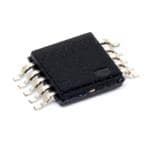
| 描述 | IC DAC 12BIT QUAD VOUT 10-MSOP数模转换器- DAC IC 12-BIT QUAD 8uS |
| 产品分类 | |
| 品牌 | Analog Devices |
| 产品手册 | |
| 产品图片 |
|
| rohs | 符合RoHS无铅 / 符合限制有害物质指令(RoHS)规范要求 |
| 产品系列 | 数据转换器IC,数模转换器- DAC,Analog Devices AD5324BRMZ- |
| 数据手册 | |
| 产品型号 | AD5324BRMZ |
| 产品培训模块 | http://www.digikey.cn/PTM/IndividualPTM.page?site=cn&lang=zhs&ptm=19145http://www.digikey.cn/PTM/IndividualPTM.page?site=cn&lang=zhs&ptm=18614http://www.digikey.cn/PTM/IndividualPTM.page?site=cn&lang=zhs&ptm=26125http://www.digikey.cn/PTM/IndividualPTM.page?site=cn&lang=zhs&ptm=26140http://www.digikey.cn/PTM/IndividualPTM.page?site=cn&lang=zhs&ptm=26150http://www.digikey.cn/PTM/IndividualPTM.page?site=cn&lang=zhs&ptm=26147 |
| 产品目录页面 | |
| 产品种类 | 数模转换器- DAC |
| 位数 | 12 |
| 供应商器件封装 | 10-MSOP |
| 分辨率 | 12 bit |
| 包装 | 管件 |
| 商标 | Analog Devices |
| 安装类型 | 表面贴装 |
| 安装风格 | SMD/SMT |
| 封装 | Tube |
| 封装/外壳 | 10-TFSOP,10-MSOP(0.118",3.00mm 宽) |
| 封装/箱体 | MSOP-10 |
| 工作温度 | -40°C ~ 105°C |
| 工厂包装数量 | 50 |
| 建立时间 | 8µs |
| 接口类型 | SPI |
| 数据接口 | DSP,MICROWIRE™,QSPI™,串行,SPI™ |
| 最大功率耗散 | 5 mW |
| 最大工作温度 | + 105 C |
| 最小工作温度 | - 40 C |
| 标准包装 | 50 |
| 电压参考 | External |
| 电压源 | 单电源 |
| 电源电压-最大 | 5.5 V |
| 电源电压-最小 | 2.5 V |
| 积分非线性 | +/- 10 LSB |
| 稳定时间 | 8 us |
| 系列 | AD5324 |
| 结构 | Resistor String |
| 转换器数 | 4 |
| 转换器数量 | 4 |
| 输出数和类型 | 4 电压,单极4 电压,双极 |
| 输出类型 | Voltage |
| 采样比 | 125 kSPs |
| 采样率(每秒) | - |


- 商务部:美国ITC正式对集成电路等产品启动337调查
- 曝三星4nm工艺存在良率问题 高通将骁龙8 Gen1或转产台积电
- 太阳诱电将投资9.5亿元在常州建新厂生产MLCC 预计2023年完工
- 英特尔发布欧洲新工厂建设计划 深化IDM 2.0 战略
- 台积电先进制程称霸业界 有大客户加持明年业绩稳了
- 达到5530亿美元!SIA预计今年全球半导体销售额将创下新高
- 英特尔拟将自动驾驶子公司Mobileye上市 估值或超500亿美元
- 三星加码芯片和SET,合并消费电子和移动部门,撤换高东真等 CEO
- 三星电子宣布重大人事变动 还合并消费电子和移动部门
- 海关总署:前11个月进口集成电路产品价值2.52万亿元 增长14.8%


PDF Datasheet 数据手册内容提取
2.5 V to 5.5 V, 500 μA, Quad Voltage Output 12-Bit DAC in 10-Lead Package AD5324-EP FEATURES GENERAL DESCRIPTION Enhanced product features The AD5324-EP1 is a quad 12-bit buffered voltage output DAC Supports defense and aerospace applications (AQEC) in a 10-lead MSOP package that operates from a single 2.5 V to Military temperature range (−55°C to +125°C) 5.5 V supply, consuming 500 μA at 3 V. Its on-chip output Controlled manufacturing baseline amplifiers allows rail-to-rail output swing to be achieved with a One assembly/test site slew rate of 0.7 V/μs. A 3-wire serial interface is used; it operates One fabrication site at clock rates up to 30 MHz and is compatible with standard SPI, Enhanced product change notification QSPI™, MICROWIRE™, and DSP interface standards. Qualification data available on request The references for the four DACs are derived from one reference 4 buffered 12-Bit DACs in 10-lead MSOP pin. The outputs of all DACs can be updated simultaneously using S Version: ±10 LSB INL the software LDAC function. The part incorporates a power-on Low power operation: 500 μA @ 3 V, 600 μA @ 5 V reset circuit, and ensures that the DAC outputs power up to 0 V 2.5 V to 5.5 V power supply and remains there until a valid write takes place to the device. Guaranteed monotonic by design over all codes The part contains a power-down feature that reduces the current Power-down to 80 nA @ 3 V, 200 nA @ 5 V consumption of the device to 200 nA at 5 V (80 nA at 3 V). Double-buffered input logic Output range: 0 V to V The low power consumption of this part in normal operation REF Power-on reset to 0 V makes it ideally suited to portable battery-operated equipment. The Simultaneous update of outputs (LDAC function) power consumption is 3 mW at 5 V, and 1.5 mW at 3 V, reducing On-chip, rail-to-rail output buffer amplifiers to 1 μW in power-down mode. Temperature range –55°C to +125°C Full details about this enhanced product are available in the APPLICATIONS AD5324 data sheet, which should be consulted in conjunction with this data sheet. Portable battery-powered instruments Digital gain and offset adjustment 1 Protected by U.S. Patent No. 5,969,657; other patents pending. Programmable voltage and current sources Programmable attenuators Industrial process control FUNCTIONAL BLOCK DIAGRAM VDD REFIN AD5324-EP LDAC BUFFER INPUT DAC STRING REGISTER REGISTER DAC A VOUTA BUFFER SCLK INPUT DAC STRING E REGISTER REGISTER DAC B VOUTB C AC SYNC TERFLOGI INPUT DAC STRING BUFFER IN REGISTER REGISTER DAC C VOUTC DIN BUFFER INPUT DAC STRING REGISTER REGISTER DAC D VOUTD POWER-ON RESET POWER-DOWN LOGIC GND 08971-001 Figure 1. Rev. 0 Information furnished by Analog Devices is believed to be accurate and reliable. However, no responsibility is assumed by Analog Devices for its use, nor for any infringements of patents or other One Technology Way, P.O. Box 9106, Norwood, MA 02062-9106, U.S.A. rights of third parties that may result from its use. Specifications subject to change without notice. No license is granted by implication or otherwise under any patent or patent rights of Analog Devices. Tel: 781.329.4700 www.analog.com Trademarks and registered trademarks are the property of their respective owners. Fax: 781.461.3113 ©2010 Analog Devices, Inc. All rights reserved.
AD5324-EP TABLE OF CONTENTS Features .............................................................................................. 1 Timing Characteristics .................................................................5 Applications ....................................................................................... 1 Absolute Maximum Ratings ............................................................6 General Description ......................................................................... 1 ESD Caution...................................................................................6 Functional Block Diagram .............................................................. 1 Pin Configuration and Function Descriptions ..............................7 Revision History ............................................................................... 2 Typical Performance Characteristics ..............................................8 Specifications ..................................................................................... 3 Outline Dimensions ....................................................................... 11 AC Characteristics ........................................................................ 4 Ordering Guide .......................................................................... 11 REVISION HISTORY 4/10—Revision 0: Initial Version Rev. 0 | Page 2 of 12
AD5324-EP SPECIFICATIONS V = 2.5 V to 5.5 V; V = 2 V; R = 2 kΩ to GND; C = 200 pF to GND; all specifications T to T , unless otherwise noted. DD REF L L MIN MAX Table 1. S Version Parameter Min Typ Max Unit Conditions/Comments DC PERFORMANCE1 Resolution 12 Bits Relative Accuracy ±2 ±10 LSB Differential Nonlinearity2 ±0.2 ±1 LSB Guaranteed monotonic by design over all codes Offset Error ±0.4 ±3 % of FSR See Figure 2 Gain Error ±0.15 ±1 % of FSR See Figure 2 Lower Dead Band 20 60 mV Lower dead band exists only if offset error is negative Offset Error Drift3 –12 ppm of FSR/°C Gain Error Drift3 –5 ppm of FSR/°C DC Power Supply Rejection Ratio3 –60 dB ΔV = ±10% DD DC Crosstalk3 200 μV R = 2 kΩ to GND or V L DD DAC REFERENCE INPUTS3 V Input Range 0.25 V V REF DD V Input Impedance 37 45 kΩ Normal operation REF >10 MΩ Power-down mode Reference Feedthrough –90 dB Frequency = 10 kHz OUTPUT CHARACTERISTICS3 Minimum Output Voltage4 0.001 V Measurement of the minimum and maximum Maximum Output Voltage4 V – 0.001 V drive capability of the output amplifier DD DC Output Impedance 0.5 Ω Short Circuit Current 25 mA V = 5 V DD 16 mA V = 3 V DD Power-Up Time 2.5 μs Coming out of power-down mode V = 5 V DD 5 μs Coming out of power-down mode V = 3 V DD LOGIC INPUTS3 Input Current ±1 μA V , Input Low Voltage 0.8 V V = 5 V ± 10% IL DD 0.6 V V = 3 V ± 10% DD 0.5 V V = 2.5 V DD V , Input High Voltage 2.4 V V = 5 V ± 10% IH DD 2.1 V V = 3 V ± 10% DD 2.0 V V = 2.5 V DD Pin Capacitance 3 pF POWER REQUIREMENTS V 2.5 5.5 V DD I (Normal Mode)5 DD V = 4.5 V to 5.5 V 600 900 μA V = V and V = GND DD IH DD IL V = 2.5 V to 3.6 V 500 700 μA V = V and V = GND DD IH DD IL I (Power-Down Mode) DD V = 4.5 V to 5.5 V 0.2 1 μA V = V and V = GND DD IH DD IL V = 2.5 V to 3.6 V 0.08 1 μA V = V and V = GND DD IH DD IL 1 DC specifications tested with the outputs unloaded. 2 Linearity is tested using a reduced code range: Code 115 to Code 3981. 3 Guaranteed by design and characterization, not production tested. 4 For the amplifier output to reach its minimum voltage, offset error must be negative. For the amplifier output to reach its maximum voltage, V = V and offset plus REF DD gain error must be positive. 5 I specification is valid for all DAC codes; interface inactive; all DACs active; load currents excluded. DD Rev. 0 | Page 3 of 12
AD5324-EP AC CHARACTERISTICS V = 2.5 V to 5.5 V; R = 2 kΩ to GND; C = 200 pF to GND; all specifications T to T , unless otherwise noted. DD L L MIN MAX Table 2. S Version2 Parameter1 Min Typ Max Unit Conditions/Comments Output Voltage Settling Time V = V = 5 V REF DD 8 10 μs ¼ scale to ¾ scale change (0x400 to 0xC00) Slew Rate 0.7 V/μs Major-Code Transition Glitch Energy 12 nV-sec 1 LSB change around major carry Digital Feedthrough 1 nV-sec Digital Crosstalk 1 nV-sec DAC-to-DAC Crosstalk 3 nV-sec Multiplying Bandwidth 200 kHz V = 2 V ± 0.1 V p-p REF Total Harmonic Distortion –70 dB V = 2.5 V ± 0.1 V p-p; frequency = 10 kHz REF 1 Guaranteed by design and characterization, not production tested. 2 Temperature range (S Version): −55°C to +125°C; typical at +25°C. Rev. 0 | Page 4 of 12
AD5324-EP TIMING CHARACTERISTICS V = 2.5 V to 5.5 V; all specifications T to T , unless otherwise noted. DD MIN MAX Table 3. Limit at T , T MIN MAX Parameter1, 2, 3 V = 2.5 V to 3.6 V V = 3.6 V to 5.5 V Unit Conditions/Comments DD DD t 40 33 ns min SCLK cycle time 1 t 16 13 ns min SCLK high time 2 t 16 13 ns min SCLK low time 3 t 16 13 ns min SYNC to SCLK falling edge setup time 4 t 5 5 ns min Data setup time 5 t 4.5 4.5 ns min Data hold time 6 t 0 0 ns min SCLK falling edge to SYNC rising edge 7 t 80 33 ns min Minimum SYNC high time 8 1 Guaranteed by design and characterization, not production tested. 2 All input signals are specified with tr = tf = 5 ns (10% to 90 % of V ) and timed from a voltage level of (V + V )/2. DD IL IH 3 See Figure 2. t1 SCLK t8 t4 t3 t2 t7 SYNC t6 t5 DIN DB15 DB0 00929-002 Figure 2. Serial Interface Timing Diagram Rev. 0 | Page 5 of 12
AD5324-EP ABSOLUTE MAXIMUM RATINGS T = 25°C, unless otherwise noted. A Stresses above those listed under Absolute Maximum Ratings may cause permanent damage to the device. This is a stress Table 4. rating only; functional operation of the device at these or any Parameter1 Rating other conditions above those indicated in the operational V to GND –0.3 V to +7 V DD section of this specification is not implied. Exposure to absolute Digital Input Voltage to GND –0.3 V to V + 0.3 V DD maximum rating conditions for extended periods may affect Reference Input Voltage to GND –0.3 V to V + 0.3 V DD device reliability. V A through V D to GND –0.3 V to V + 0.3 V OUT OUT DD Operating Temperature Range ESD CAUTION Industrial (EP Version) –55°C to +125°C Storage Temperature Range –65°C to +150°C Junction Temperature (T max) 150°C J 10-Lead MSOP Power Dissipation (TJ max – TA)/ θJA θ Thermal Impedance 206°C/W JA θ Thermal Impedance 44°C/W JC Reflow Soldering Peak Temperature 220°C Time at Peak Temperature 10 sec to 40 sec 1 Transient currents of up to 100 mA do not cause SCR latch-up. Rev. 0 | Page 6 of 12
AD5324-EP PIN CONFIGURATION AND FUNCTION DESCRIPTIONS VDD 1 10 SYNC VOUTA 2 AD5324-EP 9 SCLK VOUTB 3 TOP VIEW 8 DIN VROEUFTICN 45 (Not to Scale) 76 GVONUDTD 08971-003 Figure 3. MSOP Pin Configuration Table 5. Pin Function Descriptions Pin No. Mnemonic Description 1 V Power Supply Input. This part can be operated from 2.5 V to 5.5 V and the supply can be decoupled to GND. DD 2 V A Buffered Analog Output Voltage from DAC A. The output amplifier has rail-to-rail operation. OUT 3 V B Buffered Analog Output Voltage from DAC B. The output amplifier has rail-to-rail operation. OUT 4 V C Buffered Analog Output Voltage from DAC C. The output amplifier has rail-to-rail operation. OUT 5 REFIN Reference Input Pin for All Four DACs. It has an input range from 0.25 V to V . DD 6 V D Buffered Analog Output Voltage from DAC D. The output amplifier has rail-to-rail operation. OUT 7 GND Ground Reference Point for All Circuitry on the Part. 8 DIN Serial Data Input. This device has a 16-bit shift register. Data is clocked into the register on the falling edge of the serial clock input. The DIN input buffer is powered down after each write cycle. 9 SCLK Serial Clock Input. Data is clocked into the input shift register on the falling edge of the serial clock input. Data can be transferred at clock speeds up to 30 MHz. The SCLK input buffer is powered down after each write cycle. 10 SYNC Active Low Control Input. This is the frame synchronization signal for the input data. When SYNC goes low, it enables the input shift register and data is transferred in on the falling edges of the following 16 clocks. If SYNC is taken high before the 16th falling edge of SCLK, the rising edge of SYNC acts as an interrupt and the write sequence is ignored by the device. Rev. 0 | Page 7 of 12
AD5324-EP TYPICAL PERFORMANCE CHARACTERISTICS 12 2.0 TA = 25°C MAX INL VDD = 5V 1.5 8 1.0 OR (LSB) 04 R (LSB) 0.05 MMAINX D DNNLL R O R R L E ER 0.5 IN –4 1.0 –8 1.5 MIN INL –12 2.0 0 500 1000 1500 C2O00D0E 2500 3000 3500 4000 08971-004 80 60 40 20 T0EMPE20RATU4R0E (°6C0) 80 100 120 140 08971-023 Figure 4. Typical INL Plot Figure 7. INL and DNL Error vs. Temperature 1.0 0.2 VTAD D= =2 55°VC 0.1 VTAR E=F 2=5 °2CV GAIN ERROR 0.5 0 B) ROR (LS 0 OR (%) ––00..21 R R E R NL E –0.3 D –0.5 –0.4 OFFSET ERROR –0.5 –1.00 500 1000 1500 C2O00D0E 2500 3000 3500 4000 08971-005 –0.60 1 2 VDD3 (V) 4 5 6 08971-008 Figure 5. Typical DNL Plot Figure 8. Offset Error and Gain Error vs. V DD 0.8 5 0.7 5V SOURCE 0.6 4 0.5 GAIN ERROR ROR (%) 00..34 (V)OUT 3 3V SOURCE R V E 0.2 2 0.1 3V SINK 5V SINK 0 OFFSET ERROR 1 –0.1 –0.2 0 –80 –60 –40 –20 T0EMPE2R0ATU4R0E(°6C0) 80 100 120 140 08971-022 0 1 SINK2/SOURCE 3CURRENT4 (mA) 5 6 08971-009 Figure 6. Offset Error and Gain Error vs. Temperature Figure 9. V Source and Sink Current Capability OUT Rev. 0 | Page 8 of 12
AD5324-EP 600 1000 TA = 25°C VDD = 5V TA = 25°C 500 VREF = 2V 900 400 800 A) A) VDD = 5V (µD 300 (µD 700 D D I I 200 600 VDD = 3V 500 100 400 0 ZERO SCALE CODE FULL SCALE 08971-010 0 0.5 1.0 1.5 2.0VLO2G.I5C (V)3.0 3.5 4.0 4.5 5.0 08971-013 Figure 10. Supply Current vs. DAC Code Figure 13. Supply Current vs. Logic Input Voltage 600 TA = 25°C –40°C VDD = 5V 500 VREF = 5V 400 +25°C CH1 VOUTA +105°C A) µ (D 300 D I 200 SCLK CH2 100 02.5 3.0 3.5 VD4D.0 (V) 4.5 5.0 5.5 08971-011 CH1 1V, CH2 5V, TIME BASE = 1µs/DIV 08971-014 Figure 11. Supply Current vs. Supply Voltage Figure 14. Half-Scale Settling (¼ to ¾ Scale Code Change) 0.5 TA = 25°C VDD = 5V VREF = 2V 0.4 CH1 VDD 0.3 A) µ (D –40°C D I 0.2 +25°C CH2 VOUTA 0.1 +105°C 02.5 3.0 3.5 VD4D.0 (V) 4.5 5.0 5.5 08971-012 CH1 2V, CH2 200mV, TIME BASE = 200µs/DIV 08971-015 Figure 12. Power-Down Current vs. Supply Voltage Figure 15. Power-On Reset to 0 V Rev. 0 | Page 9 of 12
AD5324-EP 10 TA = 25°C VDD = 5V VREF = 2V 0 CH1 VOUTA –10 –20 B) d ( –30 CH2 SCLK –40 –50 CH1 500mV, CH2 5V, TIME BASE = 1µs/DIV 08971-016 –6010 100 1kFREQU1E0NkCY (Hz1)00k 1M 10M 08971-019 Figure 16. Exiting Power-Down to Midscale Figure 19. Multiplying Bandwidth (Small-Signal Frequency Response) 0.02 VDD = 5V TA = 25°C V) 0.01 Y VDD = 3V VDD = 5V OR ( FREQUENC SCALE ERR 0 L- L U F–0.01 300 350 400 I4D5D0 (µA) 500 550 600 08971-017 –0.020 1 2 VRE3F (V) 4 5 6 08971-020 Figure 17. I Histogram with V = 3 V and V = 5 V Figure 20. Full-Scale Error vs. V DD DD DD REF 2.50 2.49 V) DIV (UT mV/ VO 1 2.48 2.47 1µs/DIV 08971-018 150ns/DIV 08971-021 Figure 18. Major-Code Transition Glitch Energy Figure 21. DAC-to-DAC Crosstalk Rev. 0 | Page 10 of 12
AD5324-EP OUTLINE DIMENSIONS 3.10 3.00 2.90 3.10 10 6 5.15 3.00 4.90 2.90 4.65 1 5 PIN 1 0.50 BSC 0.95 0.85 1.10 MAX 0.75 0.80 00..1055 00..3137 SPELAANTIENG 00..2038 80°° 00..6400 COPLANARITY 0.10 COMPLIANT TO JEDEC STANDARDS MO-187-BA Figure 22. 10-Lead Mini Small Outline Package [MSOP] (RM-10) Dimensions shown in millimeters ORDERING GUIDE Model1 Temperature Range Package Description Package Option Branding AD5324SRMZ-EP-RL7 –55°C to +125°C 10-Lead Mini Small Outline Package (MSOP) RM-10 DFT 1 Z = RoHS Compliant Part. Rev. 0 | Page 11 of 12
AD5324-EP NOTES ©2010 Analog Devices, Inc. All rights reserved. Trademarks and registered trademarks are the property of their respective owners. D08971-0-4/10(0) Rev. 0 | Page 12 of 12
Mouser Electronics Authorized Distributor Click to View Pricing, Inventory, Delivery & Lifecycle Information: A nalog Devices Inc.: AD5324ACPZ-REEL7 AD5324BRMZ-REEL7 AD5324ARMZ AD5324ARMZ-REEL7 AD5324BRM-REEL7 AD5324BRMZ AD5324BRM AD5324ARM AD5324BCPZ-REEL7 AD5324SRMZ-EP-RL7 AD5324BRMZ-REEL EVAL-AD5324DBZ