ICGOO在线商城 > 集成电路(IC) > 数据采集 - 数模转换器 > DAC8571IDGK
 Datasheet下载
- 型号: DAC8571IDGK
- 制造商: Texas Instruments
- 库位|库存: xxxx|xxxx
- 要求:
| 数量阶梯 | 香港交货 | 国内含税 |
| +xxxx | $xxxx | ¥xxxx |
查看当月历史价格
查看今年历史价格
DAC8571IDGK产品简介:
ICGOO电子元器件商城为您提供DAC8571IDGK由Texas Instruments设计生产,在icgoo商城现货销售,并且可以通过原厂、代理商等渠道进行代购。 DAC8571IDGK价格参考¥21.81-¥40.53。Texas InstrumentsDAC8571IDGK封装/规格:数据采集 - 数模转换器, 16 位 数模转换器 1 8-VSSOP。您可以下载DAC8571IDGK参考资料、Datasheet数据手册功能说明书,资料中有DAC8571IDGK 详细功能的应用电路图电压和使用方法及教程。
Texas Instruments(德州仪器)的DAC8571IDGK是一款高精度、低功耗的16位数模转换器(DAC),广泛应用于需要高分辨率和精确模拟信号输出的各种场景。以下是该型号的主要应用场景:

 1. 工业自动化与控制
   DAC8571IDGK在工业自动化系统中用于将数字信号转换为模拟信号,以实现对电机、阀门、传感器等设备的精确控制。例如,在自动化生产线中,DAC可以用于调节温度、压力、流量等参数,确保生产过程的稳定性和精度。

 2. 精密测量与测试设备
   在精密测量仪器和测试设备中,DAC8571IDGK能够提供高精度的电压或电流输出,用于校准和验证其他设备的性能。它常用于实验室中的数据采集系统、示波器、频谱分析仪等设备,确保测量结果的准确性。

 3. 医疗设备
   医疗设备如心电图机、超声波设备、监护仪等需要高精度的模拟信号来处理生物电信号。DAC8571IDGK可以用于这些设备中的信号调理电路,确保信号的准确性和稳定性,从而提高诊断和治疗的可靠性。

 4. 通信系统
   在通信领域,DAC8571IDGK可用于生成高质量的模拟信号,特别是在无线通信基站、调制解调器和其他射频(RF)设备中。它可以用于信号调制、频率合成等关键环节,确保通信系统的高效运行。

 5. 音频处理
   DAC8571IDGK还可以应用于高端音频设备中,如专业音响、录音设备等。其高精度的数模转换能力可以确保音频信号的保真度,提供更清晰、更真实的音质体验。

 6. 电力电子
   在电力电子领域,DAC8571IDGK可用于逆变器、变频器等设备中,实现对电压、电流的精确控制。通过调节输出信号,可以优化电力系统的效率和稳定性,减少能量损耗。

 7. 汽车电子
   现代汽车中的许多系统依赖于高精度的模拟信号,如发动机控制单元(ECU)、车身控制系统等。DAC8571IDGK可以用于这些系统中,确保车辆各个部件的协调工作,提升驾驶体验和安全性。

总之,DAC8571IDGK凭借其高精度、低功耗和灵活性,适用于多种对模拟信号要求苛刻的应用场合,尤其在工业、医疗、通信等领域表现出色。
| 参数 | 数值 |
| 产品目录 | 集成电路 (IC)半导体 |
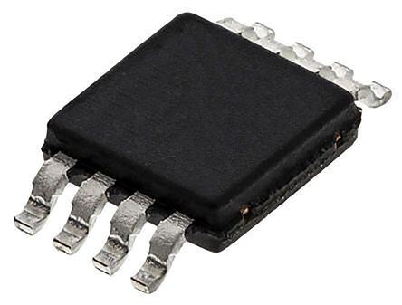
| 描述 | IC DAC 16BIT I2C V-OUT LP 8VSSOP数模转换器- DAC Lo-Pwr R-To-R Output 16-Bit I2C Input |
| 产品分类 | |
| 品牌 | Texas Instruments |
| 产品手册 | http://www.ti.com/litv/slas373a |
| 产品图片 |
|
| rohs | 符合RoHS无铅 / 符合限制有害物质指令(RoHS)规范要求 |
| 产品系列 | 数据转换器IC,数模转换器- DAC,Texas Instruments DAC8571IDGK- |
| 数据手册 | |
| 产品型号 | DAC8571IDGK |
| 产品培训模块 | http://www.digikey.cn/PTM/IndividualPTM.page?site=cn&lang=zhs&ptm=13240 |
| 产品目录页面 | |
| 产品种类 | 数模转换器- DAC |
| 位数 | 16 |
| 供应商器件封装 | 8-VSSOP |
| 其它名称 | 296-26051-5 |
| 分辨率 | 16 bit |
| 制造商产品页 | http://www.ti.com/general/docs/suppproductinfo.tsp?distId=10&orderablePartNumber=DAC8571IDGK |
| 包装 | 管件 |
| 单位重量 | 26 mg |
| 商标 | Texas Instruments |
| 安装类型 | 表面贴装 |
| 安装风格 | SMD/SMT |
| 封装 | Tube |
| 封装/外壳 | 8-TSSOP,8-MSOP(0.118",3.00mm 宽) |
| 封装/箱体 | VSSOP-8 |
| 工作温度 | -40°C ~ 105°C |
| 工厂包装数量 | 80 |
| 建立时间 | 12µs |
| 接口类型 | Serial (2-Wire, I2C) |
| 数据接口 | I²C |
| 最大工作温度 | + 105 C |
| 最小工作温度 | - 40 C |
| 标准包装 | 80 |
| 电压参考 | External |
| 电压源 | 单电源 |
| 电源电压-最大 | 5.5 V |
| 电源电压-最小 | 2.7 V |
| 积分非线性 | +/- 0.098 % FSR |
| 稳定时间 | 15 us |
| 系列 | DAC8571 |
| 结构 | Resistor-String |
| 转换器数 | 1 |
| 转换器数量 | 1 |
| 输出数和类型 | 1 电压,单极 |
| 输出类型 | Voltage |
| 配用 | /product-detail/zh/DAC8571EVM/296-19942-ND/608271 |
| 采样比 | 43 kSPs |
| 采样率(每秒) | 43k |


- 商务部:美国ITC正式对集成电路等产品启动337调查
- 曝三星4nm工艺存在良率问题 高通将骁龙8 Gen1或转产台积电
- 太阳诱电将投资9.5亿元在常州建新厂生产MLCC 预计2023年完工
- 英特尔发布欧洲新工厂建设计划 深化IDM 2.0 战略
- 台积电先进制程称霸业界 有大客户加持明年业绩稳了
- 达到5530亿美元!SIA预计今年全球半导体销售额将创下新高
- 英特尔拟将自动驾驶子公司Mobileye上市 估值或超500亿美元
- 三星加码芯片和SET,合并消费电子和移动部门,撤换高东真等 CEO
- 三星电子宣布重大人事变动 还合并消费电子和移动部门
- 海关总署:前11个月进口集成电路产品价值2.52万亿元 增长14.8%


PDF Datasheet 数据手册内容提取
3 mm x 5 mm DAC8571 www.ti.com SLAS373A–DECEMBER2002–REVISEDJULY2003 2 16-BIT, LOW POWER, VOLTAGE OUTPUT, I C INTERFACE DIGITAL-TO-ANALOG CONVERTER FEATURES DESCRIPTION • MicropowerOperation:160µA@5V The DAC8571 is a small low-power, 16-bit voltage • Power-OnResettoZero output DAC with an I2C compatible two-wire serial • SingleSupply:+2.7Vto+5.5V interface. Its on-chip precision output amplifier allows • 16-BitMonotonic rail-to-rail output swing and settles within 10 microseconds. The DAC8571 architecture is 16-bit • SettlingTime:10µsto–0.003% FSR monotonic, and factory trimming typically achieves –4 • I2C™InterfaceWithHigh-SpeedMode mV absolute accuracy at all codes. The DAC8571 • SupportsDataReceiveandTransmit requires an external reference voltage to set its • On-ChipRail-to-RailOutputBuffer outputvoltagerange. • Double-BufferedInputRegister The low power consumption and small size of this • SupportsSynchronousMultichannelUpdate part make it ideally suited to portable battery • OffsetError:–1 mVmaxat25(cid:176)C operated equipment. The power consumption is typi- cally 800 µW at V = 5 V reducing to 1 µW in • Full-ScaleError:–3 mVmaxat25(cid:176)C DD power-downmode. • Small8LeadMSOPPackage The DAC8571 incorporates a 2-wire I2C interface. APPLICATIONS Standard, fast, and high-speed modes of I2C oper- ation are all supported up to 3.4 MHz serial clock • ProcessControl speeds. Multichannel synchronous data update and • DataAcquisitionSystems power-downoperationsaresupportedthrough the I2C • Closed-LoopServoControl bus. DAC8571 is also capable of transmitting the • PCPeripherals contents of its serial shift register, a key feature for I2Csystemverification. • PortableInstrumentation The DAC8571 is available in an 8-lead MSOP pack- ageandisspecifiedover-40(cid:176)C to105(cid:176)C. VREF V(SENSE) _ Ref + 16 Bit DAC + VOUT VDD 16 DAC Register Temporary Register SDA Power Down Resistor SCL I2C Block Control Logic Network A0 GND Pleasebeawarethatanimportantnoticeconcerningavailability,standardwarranty,anduseincriticalapplicationsofTexas Instrumentssemiconductorproductsanddisclaimerstheretoappearsattheendofthisdatasheet. I2CisatrademarkofPhilipsCorporation. PRODUCTIONDATAinformationiscurrentasofpublicationdate. Copyright©2002–2003,TexasInstrumentsIncorporated Products conform to specifications per the terms of the Texas Instruments standard warranty. Production processing does not necessarilyincludetestingofallparameters.
DAC8571 www.ti.com SLAS373A–DECEMBER2002–REVISEDJULY2003 These devices have limited built-in ESD protection. The leads should be shorted together or the device placedinconductivefoamduringstorageorhandlingtopreventelectrostaticdamagetotheMOSgates. PINCONFIGURATIONS VDD 1 8 GND VREF 2 7 SDA V(SENSE) 3 6 SCL VOUT 4 5 A0 PINDESCRIPTION Pin Name Function 1 V Analogvoltagesupplyinput DD 2 V Positivereferencevoltageinput REF 3 V Analogoutputsense (SENSE) 4 V AnalogoutputvoltagefromDAC OUT 5 A0 Deviceaddressselect 6 SCL Serialclockinput 7 SDA Serialdatainput/output 8 GND Groundreferencepointforallcircuitryonthepart PACKAGE/ORDERINGINFORMATION Transport Package SpecifiedTemperature Package Product Package OrderingNumber Media, Designator Range Marking Quantity Tube,80 DAC8571 8-MSOP DGK -40(cid:176)C to+105(cid:176)C D871 DAC8571IDGK Tape&Reel, DAC8571IDGKR 2500 ABSOLUTE MAXIMUM RATINGS(1) UNITS V toGND -0.3Vto+6V DD DigitalinputvoltagetoGND -0.3VtoV +0.3V DD V toGND -0.3Vto+V +0.3V OUT DD Operatingtemperaturerange -40(cid:176)C to+105(cid:176)C Storagetemperaturerange -65(cid:176)C to+150(cid:176)C Junctiontemperaturerange(Tmax) +150(cid:176)C J Q Thermalimpedance 260(cid:176)C/W JA Q Thermalimpedance 44(cid:176)C/W JC Vaporphase(60s) 215(cid:176)C Leadtemperature,soldering Infrared(15s) 220(cid:176)C (1) Stressesabovethoselistedunder“AbsoluteMaximumRatings”maycausepermanentdamagetothedevice.Exposuretoabsolute maximumconditionsforextendedperiodsmayaffectdevicereliability. 2
DAC8571 www.ti.com SLAS373A–DECEMBER2002–REVISEDJULY2003 ELECTRICAL CHARACTERISTICS V =+2.7Vto+5.5V;R =2kW toGND;C =200pFtoGND;lowpowermode;allspecifications-40(cid:176)C to105(cid:176)C (unless DD L L otherwisenoted) DAC8571 PARAMETER CONDITIONS MIN TYP MAX UNITS STATICPERFORMANCE (1) Resolution 16 Bits Relativeaccuracy –0.098 %ofFSR Differentialnonlinearity Monotonicbydesign –0.25 –1 LSB Offseterror Measuredatcode485,25(cid:176)C 0.3 –1.0 mV Measuredatcode485,-40(cid:176)C...105 (cid:176)C 1.0 –5.0 Full-scaleerror Measuredatcode64714,25(cid:176)C 0.5 –3.0 mV Measuredatcode64714,-40(cid:176)C...105 (cid:176)C 1.0 –5.0 Gainerror Measuredatcode64714,25(cid:176)C 1.0 –3.0 mV Measuredatcode64714,-40(cid:176)C...105 (cid:176)C 2.0 –5.0 Zerocodeerrordrift AllzeroesloadedtoDACregister -20 µV/(cid:176)C Gaintemperaturecoefficient -5 ppmofFSR/(cid:176)C Absoluteaccuracy Allcodesfromcode485tocode64714,25(cid:176)C –2.5 mV Allcodesfromcode485tocode64714, –3.5 -40(cid:176)C...105 (cid:176)C OUTPUTCHARACTERISTICS(2) Outputvoltagerange 0 V V REF Outputvoltagesettlingtime(full R =2kW; C <200pF,fastsettling 8 10 µs L L scale) R =2kW; C =500pF,fastsettling 12 µs L L R =2kW; C <200pF,lowpower 13 15 µs L L Slewrate R =2kW; C <200pF,fastsettling 1 V/µs L L R =2kW; C <200pF,lowpower 0.5 L L Capacitiveloadstability R =¥ 470 pF L R =2kW 1000 pF L Digital-to-analogglitchimpulse 20 nV-s Digitalfeedthrough 0.5 nV-s DCoutputimpedance 1 W Shortcircuitcurrent V =+5V 50 mA DD V =+3V 20 mA DD Power-uptime Comingoutofpower-downmode,V =+5V 2.5 µs DD Comingoutofpower-downmode,V =+3V 5 µs DD PSRR 0.75 mV/V REFERENCEINPUT V inputrange 0 V V REFH DD Referenceinputimpedance 140 kW LOGICINPUTS (2) Inputcurrent –1 µA V ,Inputlowvoltage V =2.7-5.5V 0.3V V IN_L DD DD V ,Inputhighvoltage V =2.7-5.5V 0.7V V IN_H0 DD DD Pincapacitance 3 pF POWERREQUIREMENTS V 2.7 5.5 V DD I (normaloperation) DACactive,I included DD ref (1) Linearitycalculatedusingareducedcoderangeof485to64714.Outputunloaded. (2) Assuredbydesignandcharacterization,notproductiontested. 3
DAC8571 www.ti.com SLAS373A–DECEMBER2002–REVISEDJULY2003 ELECTRICAL CHARACTERISTICS (continued) V =+2.7Vto+5.5V;R =2kW toGND;C =200pFtoGND;lowpowermode;allspecifications-40(cid:176)C to105(cid:176)C (unless DD L L otherwisenoted) DAC8571 PARAMETER CONDITIONS MIN TYP MAX UNITS V =+4.5Vto+5.5V V =V ,V =GND,fastsettling 250 400 µA DD IH DD IL V =V ,V =GND,lowpower 160 225 IH DD IL V =+2.7Vto+3.6V V =V ,V =GND,fastsettling 240 380 µA DD IH DD IL V =V ,V =GND,lowpower 140 200 IH DD IL I (allpower-downmodes) DACactive,I included DD ref V =+4.5Vto+5.5V V =V andV =GND 0.2 1 µA DD IH DD IL V =+2.7Vto+3.6V V =V andV =GND 0.05 1 µA DD IH DD IL POWEREFFICIENCY I /I I =2mA,V =+5V 93% OUT DD L DD TIMING CHARACTERISTICS V =+2.7Vto+5.5V;R =2kW toGND;allspecifications-40(cid:176)C to105(cid:176)C (unlessotherwisenoted) DD L SYMBOL PARAMETER TESTCONDITIONS MIN TYP MAX UNITS Standardmode 100 kHz Fastmode 400 kHz t SCLclockfrequency SCL High-speedmode,C -100pFmax 3.4 MHz B High-speedmode,C -400pFmax 1.7 MHz B BusfreetimebetweenaSTOPand Standardmode 4.7 µs t BUF STARTcondition Fastmode 1.3 µs Standardmode 4.0 \µs Holdtime(repeated)STARTcon- t ;t Fastmode 600 ns HO STA dition High-speedmode 160 ns Standardmode 4.7 µs t LOWperiodoftheSCLclock LOW Fastmode 1.3 µs Standardmode 4.0 µs Fastmode 600 ns t HIGHperiodoftheSCLclock HIGH High-speedmode,C -100pFmax 60 ns B High-speedmode,C -400pFmax 120 ns B Standardmode 4.7 µs SetuptimeforarepeatedSTART t ;t Fastmode 600 ns SU STA condition High-speedmode 160 ns Standardmode 250 ns t ;t Datasetuptime Fastmode 100 ns SU DAT High-speedmode 10 ns Standardmode 0 0.9 µs Fastmode 0 0.9 µs t ;t Dataholdtime HD DAT High-speedmode,C -100pFmax 0 70 ns B High-speedmode,C -400pFmax 0 150 ns B Standardmode 20+0.1C 1000 ns B Fastmode 20+0.1C 300 ns B t RisetimeofSCLsignal RCL High-speedmode,C -100pFmax 10 40 ns B High-speedmode,C -400pFmax 20 80 ns B 4
DAC8571 www.ti.com SLAS373A–DECEMBER2002–REVISEDJULY2003 TIMING CHARACTERISTICS (continued) V =+2.7Vto+5.5V;R =2kW toGND;allspecifications-40(cid:176)C to105(cid:176)C (unlessotherwisenoted) DD L SYMBOL PARAMETER TESTCONDITIONS MIN TYP MAX UNITS Standardmode 20+0.1C 1000 ns B RisetimeofSCLsignalaftera Fastmode 20+0.1C 300 ns B t repeatedSTARTcondition,and RCL1 afteranacknowledgeBIT High-speedmode,CB-100pFmax 10 80 ns High-speedmode,C -400pFmax 20 1600 ns B Standardmode 20+0.1C 300 ns B Fastmode 20+0.1C 300 ns B t FalltimeofSCLsignal FCL High-speedmode,C -100pFmax 10 40 ns B High-speedmode,C -400pFmax 20 80 ns B Standardmode 20+0.1C 1000 ns B Fastmode 20+0.1C 300 ns B t RisetimeofSDAsignal RCA High-speedmode,C -100pFmax 10 80 ns B High-speedmode,C -400pFmax 20 160 ns B Standardmode 20+0.1C 300 ns B Fastmode 20+0.1C 300 ns B t FalltimeofSDAsignal FDA High-speedmode,C -100pFmax 10 80 ns B High-speedmode,C -400pFmax 20 160 ns B Standardmode 4.0 µs t ;t SetuptimeforSTOPcondition Fastmode 600 ns SU STO High-speedmode 160 ns C CapacitiveloadforSDAandSCL 400 pF B Fastmode 50 ns t Pulsewidthofspikesuppressed SP High-speedmode 10 ns Standardmode NoisemarginattheHIGHlevelfor V eachconnecteddevice(including Fastmode 0.2V V NH DO hysteresis) High-speedmode Standardmode NoisemarginattheLOWlevelfor V eachconnecteddevice(including Fastmode 0.1V V NL DO hysteresis) High-speedmode 5
DAC8571 www.ti.com SLAS373A–DECEMBER2002–REVISEDJULY2003 TYPICAL CHARACTERISTICS AtT =+25(cid:176)C, unlessotherwisenoted. A DIFFERENTIALLINEARITYERRORvsDIGITALINPUT LINEARITYERRORvsDIGITALINPUTCODE CODE 64 1 0.8 48 0.6 B 32 S 0.4 L or - 16 0.2 Err 0 B 0 earity -16 E - LS -0.2 n L -0.4 Li -32 D -0.6 -48 -0.8 -64 -1 0 10000 20000 30000 40000 50000 60000 0 10000 20000 30000 40000 50000 60000 Digital Input Code Digital Input Code Figure1. Figure2. ERRORvsTEMPERATURE ERRORvsTEMPERATURE 3 3 Full–Scale VDD = 5 V VDD = 3 V 2 2 Full–Scale 1 Gain 1 V V m m Gain or – 0 Zero–Scale or – 0 Zero–Scale Err Err –1 –1 –2 –2 –3 –3 –40 –20 0 20 40 60 80 100 –40 –20 0 20 40 60 80 100 TA – Free–Air Temperature – °C TA – Free–Air Temperature – °C Figure3. Figure4. LINEARITYERROR DIFFERENTIALLINEARITYERROR vs vs TEMPERATURE TEMPERATURE 64 1 0.8 48 MAX Error B LS 0.6 MAX Error Linearity Error - LSB ---14313068262 MIN Error Differential Linearity Error - ---00000.....064224 MIN Error -0.8 -64 -1 -40 0 40 80 110 -40 0 40 80 110 TA - Free-Air Temperature - °C TA - Free-Air Temperature - °C Figure5. Figure6. 6
DAC8571 www.ti.com SLAS373A–DECEMBER2002–REVISEDJULY2003 TYPICAL CHARACTERISTICS (continued) AtT =+25(cid:176)C, unlessotherwisenoted. A SINKCURRENTATNEGATIVERAIL SOURCECURRENTATPOSITIVERAIL 0.15 5 0.125 e - V VDD = 2.7 V e - V 4.95 ag 0.1 ag Volt VDD = 5 V Volt ut 0.075 ut 4.9 p p ut ut O O - OUT 0.05 - OUT 4.85 VREF = VDD - 10 mV V 0.025 VREF = VDD - 10 mV V DAC Loaded With FFFFH DAC Loaded With 0000 V = 5 V H DD 0 4.8 0 1 2 3 4 5 0 1 2 3 4 5 I - Sink Current - mA I - Source Current - mA SINK SOURCE Figure7. Figure8. SOURCECURRENTATPOSITIVERAIL SUPPLYCURRENTvsDIGITALINPUTCODE 2.7 250 V A 200 Voltage - 2.65 murrent - 150 VDD = 5 V Output 2.6 upply C 100 VDD = 3.6 V V - OUT 2.55 VDRAECF =L oVaDdDe -d 1 W0 imthV FFFFH I - SDD 50 V = 2.7 V Reference Current Included DD 2.5 0 0 1 2 3 4 5 0 10000 20000 30000 40000 50000 60000 ISOURCE - Source Current - mA Digital Input Code Figure9. Figure10. SUPPLYCURRENTvsTEMPERATURE SUPPLYCURRENTvsSUPPLYVOLTAGE 250 140 IREF Included 120 VREF = VDD, IDD Measured at Power-Up, A 200 VDD = 5.5 V A Reference Current Included, No Load mnt – mnt - 100 urre 150 urre 80 Supply C 100 VDD = 3.6 V Supply C 60 I – DD 50 I - DD 2400 0 0 –40 –20 0 20 40 60 80 100 2.7 3.1 3.5 3.9 4.3 4.7 5.1 5.5 TA – Free–Air Temperature – °C VDD - Supply Voltage - V Figure11. Figure12. 7
DAC8571 www.ti.com SLAS373A–DECEMBER2002–REVISEDJULY2003 TYPICAL CHARACTERISTICS (continued) AtT =+25(cid:176)C, unlessotherwisenoted. A SUPPLYCURRENTvsLOGICINPUTVOLTAGE HISTOGRAMOFCURRENTCONSUMPTION 1 2500 0.9 TRAe f=e r2e5n(cid:176)cCe, CAu0rr eInnp t uInt c(lAuldl eOdther Inputs = GND) IREF Included A 0.8 2000 m nt - 0.7 VDD = VREF = 5.5 V y VDD = 2.7 V VDD = 5.5 V ply Curre 000...456 VDD = VREF = 2.7 V Frequenc 11050000 Sup 0.3 f - - DD 0.2 500 I 0.1 0 0 0 1 2 3 4 5 0 40 80 120 160 200 240 280 Logic Input Voltage - V IDD - Supply Current - m A Figure13. Figure14. EXITINGPOWER-DOWNMODE OUTPUTGLITCH(Mid-Scale) 5.5 2.5 5 4.5 V age - 3.45 div)2.45 olt 3 V/ V m utput 2.25 V, 50 2.4 O ( - OUT 1.15 VO2.35 VCroedf e= 7VFDFDF -h 5to0 8m0V00h V 0.5 (Glitch Occurs Every N x 4096 0 Code Boundary) -0.5 2.3 t - Time - 5m s/div 0 5 10 15 20 25 30 t - Time - m S Figure15. Figure16. ABSOLUTEERROR FULL-SCALESETTLINGTIME(LargeSignal) 0.005 6 0.004 VDD = 5 V usted Error - V 000...0000001230 put Voltage – V 345 VDD= =5 VVREF adj -0.001 Out Output al Un -0.002 – UT 2 Lo2a kdWed a Wndith Tot -0.003 VO 1 200 pF to -0.004 GND -0.005 0 0 10000 20000 30000 40000 50000 60000 t – Time – 12m s/div, Fast–Settling Mode Digital Input Code Figure17. Figure18. 8
DAC8571 www.ti.com SLAS373A–DECEMBER2002–REVISEDJULY2003 TYPICAL CHARACTERISTICS (continued) AtT =+25(cid:176)C, unlessotherwisenoted. A HALF-SCALESETTLINGTIME(LargeSignal) FULL-SCALESETTLINGTIME(LargeSignal) 3.0 3.5 3.0 V 2.5 V Output Voltage – 12..50 VDOD= u =5t p VVuRtEF Output Voltage – 122...505 VD=OD u2=.t 7pV uVRtEF – UT 1.0 Lo2a kdWed a Wndith – UT 1.0 Lo2a kdWed a Wndith VO 0.5 200 pF to VO 0.5 200 pF to GND GND 0.0 0.0 t – Time – 12m s/div, Fast–Settling Mode t – Time – 12m s/div, Fast–Settling Mode Figure19. Figure20. HALF-SCALESETTLINGTIME SIGNAL-TO-NOISERATIOvsOUTPUTFREQUENCY SIGNAL-TO-NOISE RATIO vs OUTPUT FREQUENCY 98 V 1.50 96 – V = 5V e DD g 94 a Output Volt 1.00 VD=OD u2=.t 7pV uVRtEF SNR (dB) 9920 VDD = 2.7V – Loaded With UT 0.50 2 kW and 88 O V 200 pF to V = V DD REF GND 86 -1dB FSR Digital Input, FS = 52ksps 0.00 Measurement Bandwidth = 20kHz t – Time – 12m s/div, Fast–Settling Mode 84 0 500 1k 1.5k 2k 2.5k 3k 3.5k 4k 4.5k Output Frequency (Hz), Fast-Settling Mode Figure21. Figure22. TOTALHARMONICDISTORTIONvsOUTPUTFREQUENCY TOTALHARMONICDISTORTIONvsOUTPUTFREQUENCY OUTPUT FREQUENCY 0 0 -10 VDD = VREF = 5V -10 VDD = VREF = 2.7V F = 52ksps, -1dB FSR Digital Input F = 52ksps,-1dB FSR Digital Input -20 MSeasurement Bandwidth = 20kHz -20 MSeasurement Bandwidth = 20kHz -30 -30 B) -40 B) -40 d THD d THD D ( -50 D ( -50 H H T -60 T -60 -70 -70 -80 -80 3rd Harmonic -90 -90 2nd Harmonic 2nd Harmonic 3rd Harmonic -100 -100 0 500 1k 1.5k 2k 2.5k 3k 3.5k 4k 0 500 1k 1.5k 2k 2.5k 3k 3.5k 4k Output Frequency (Hz), Fast-Settling Mode Output Frequency (Hz), Fast-Settling Mode Figure23. Figure24. 9
DAC8571 www.ti.com SLAS373A–DECEMBER2002–REVISEDJULY2003 TYPICAL CHARACTERISTICS (continued) AtT =+25(cid:176)C, unlessotherwisenoted. A FULL-SCALESETTLINGTIME FULL-SCALESETTLINGTIME (Small-Signal-PositiveGoingStep) (Small-Signal-NegativeGoingStep) ge Small-Signal Settling ge Small-Signal Settling Volta T5mimVe/div Volta T5mimVe/div ut ut p p ut ut O O Trigger Trigger Signal Signal Time (2m s/div) Time (2m s/div) Figure25. Figure26. 10
DAC8571 www.ti.com SLAS373A–DECEMBER2002–REVISEDJULY2003 THEORY OF OPERATION D/A SECTION The architecture of the DAC8571 consists of a string DAC followed by an output buffer amplifier. Figure 27 showsablockdiagramoftheDACarchitecture. Reference Voltage V(SENSE) Ref+ _ Resistor VOUT DAC Register + String Ref- GND Figure27.DAC8571Architecture TheinputcodingtotheDAC8571isunsignedbinary,whichgivestheidealoutputvoltageas: V (cid:2)V (cid:1) D OUT REF 65536 whereD=decimalequivalentofthebinarycodethatisloadedtotheDACregister;itcanrangefrom0to65535. RESISTOR STRING The resistor string section is shown in Figure 28. It is simply a divide-by-two resistor, followed by a string of resistors, each of value R. The code loaded into the DAC register determines at which node on the string the voltage is tapped off to be fed into the output amplifier by closing one of the switches connecting the string to the amplifier.Becauseitisastringofresistors,itisassuredmonotonic. VREF R To Output R Amplifier R R GND Figure28.ResistorString. 11
DAC8571 www.ti.com SLAS373A–DECEMBER2002–REVISEDJULY2003 THEORY OF OPERATION (continued) Output Amplifier The output buffer is a gain-of-2 noninverting amplifier capable of generating rail-to-rail voltages at its output, whichgivesan output range of 0 V to V . It is capable of driving a load of 2 kW in parallel with 1000 pF to GND. DD The source and sink capabilities (fast settling) of the output amplifier can be seen in the typical curves. The slew rate is 1 V/µs with a full-scale settling time of 10 µs with the output loaded. The feedback and gain setting resistors of the amplifier are in the order of 50 kW. Their absolute value can be off significantly, but they are matchedtowithin0.1%. The inverting input of the output amplifier is brought out to the VSENSE pin, through the feedback resistor. This allows for better accuracy in critical applications by tying the VSENSE point and the amplifier output together directly at the load. Other signal conditioning circuitry may also be connected between these points for specific applicationsincludingcurrentsourcing. I2C Interface The DAC8571 uses the I2C interface (see I2C-Bus Specification Version 2.1, January 2000, Philips Semiconductor) to receive and transmit digital data. I2C is a 2-wire serial interface that allows multiple devices on the same bus to communicate with each other. The serial bus consists of the serial data (SDA) and serial clock (SCL) lines. Connections to the SDA and SCL lines of the bus are made through open drain IO pins of each device on the bus. Since the devices that connect to the bus have open drain outputs, the bus should include pullupstructures.Whenthebusisnotactive,bothSCLandSDAlinesarepulledhighbythesepullupdevices. The DAC8571 supports the I2C serial bus and data transmission protocol, in all three defined modes: standard (100Kbps),fast(400kBps),andhighspeed(3.4Mbps). I2C specification states that the device that controls the message is called a master, and the devices that are controlled by the master are slaves. The master device generates the SCL signal. A master device also generates special timing conditions (start condition, repeated start condition, and stop condition) on the bus to indicate the start or stop of a data transfer. Device addressing is also done by the master. The master device on an I2C bus is usually a microcontroller or a digital signal processor (DSP). The DAC8571 on the other hand, operates as a slave device on the I2C bus. A slave device acknowledges master's commands and upon master's control,eitherreceivesortransmitsdata. I2C specification states that a device that sends data onto the bus is defined as a transmitter, and a device receiving data from the bus is defined as a receiver. DAC8571 normally operates as a slave receiver. A master devicewritestoDAC8571,aslavereceiver.However,ifamasterdeviceinquiresDAC8571 internal register data, DAC8571, operates as a slave transmitter. In this case, the master device reads from the DAC8571, a slave transmitter.AccordingtoI2Cterminology,readandwritearewithrespecttothemasterdevice. Other than specific timing signals, I2C interface works with serial bytes. At the end of each byte, a 9th clock cycle is used to generate/detect an acknowledge signal. An acknowledge is when the SDA line is pulled low during the high period of 9th clock cycle. A not-acknowledge is when SDA line is left high during the high period of the 9th clockcycle. SDA SCL Data Line Stable; Change of Data Allowed Data Valid Figure29.ValidData 12
DAC8571 www.ti.com SLAS373A–DECEMBER2002–REVISEDJULY2003 THEORY OF OPERATION (continued) Data Output by Transmitter Not Acknowledge Data Output by Receiver Acknowledge SCL From 1 2 8 9 Master S Clock Pulse for START Acknowledgement Condition Figure30.AcknowledgeontheI2CBus Recognize START or Recognize STOP or REPEATED START REPEATED START Condition Condition Generate ACKNOWLEDGE Signal P SDA MSB Acknowledgement Sr Signal From Slave Address R/W SCL 1 2 7 8 9 1 2 3 - 8 9 S Sr ACK ACK or or Sr P Clock Line Held Low While Interrupts are Serviced START or STOP or Repeated START Repeated START Condition Condition Figure31.BusProtocol 13
DAC8571 www.ti.com SLAS373A–DECEMBER2002–REVISEDJULY2003 Master Writing to a Slave Receiver (Standard/Fast Modes) I2C protocol starts when the bus is idle, that is, when SDA and SCL lines are stable high. The master then pulls the SDA line low while SCL is still high indicating that serial data transfer has started. This is called a start condition, and can only be asserted by the master. After the start condition, the master generates the serial clock pulses and puts out an address byte, ADDRESS<7:0>. While generating the bit stream, the master ensures the timing for valid data. For each valid I2C bit, SDA line should remain stable during the entire high period of the SCL line. The address byte consists of 7 address bits (1001100, assuming A0=0) and a direction bit (R/W=0). After sending the address byte, the master generates a 9th SCL pulse and monitors the state of the SDA line during the high period of this 9th clock cycle. The SDA line being pulled low by a receiver during the high period of 9th clock cycle is called an acknowledge signal. If the master receives an acknowledge signal, it knows that a DAC8571 successfully matched the address the master sent. Upon the receipt of this acknowledge, the master knows that the communication link with a DAC8571 has been established and more data could be sent. The master continues by sending a control byte C<7:0>, which sets DAC8571's operation mode. After sending the control byte, the master expects an acknowledge signal. Upon receipt of the acknowledge, the master sends a most significant byte M<7:0> that represents the eight most significant bits of DAC8571's 16-bit digital-to-analog conversiondata.UponreceiptoftheM<7:0>,DAC8571sendsanacknowledge.Afterreceivingthe acknowledge, the master sends a least significant byte L<7:0> that represents the eight least significant bits of DAC8571's 16-bit conversion data. After receiving the L<7:0>, the DAC8571 sends an acknowledge. At the falling edge of the acknowledge signal following the L<0>, DAC8571 performs a digital to analog conversion. For further DAC updates, the master can keep repeating M<7:0> and L<7:0> sequences, expecting an acknowledge after each byte. After the required number of digital-to-analog conversions is complete, the master can break the communicationlinkwithDAC8571bypullingtheSDA line from low to high while SCL line is high. This is called a stop condition. A stop condition brings the bus back to idle (SDA and SCL both high). A stop condition indicates that communication with DAC8571 has ended. All devices on the bus including DAC8571 then await a new start condition followed by a matching address byte. DAC8571 stays at its current state upon receipt of a stop condition. Table 1 demonstrates the sequence of events that should occur while a master transmitter is writing to DAC8571. 14
DAC8571 www.ti.com SLAS373A–DECEMBER2002–REVISEDJULY2003 Table1. MasterTransmitterWritingtoSlaveReceiver(DAC8571) Standard/FastModeWriteSequence-DataInput Transmitter MSB 6 5 4 3 2 1 LSB Comment Master Start Beginsequence Master 1 0 0 1 1 A0 0 R/W Writeaddressing(LSB=0) DAC8571 DAC8571Acknowledges Master 0 0 Load1 Load0 0 Brcsel 0 PD0 Controlbyte(PD0=0) DAC8571 DAC8571Acknowledges Master D15 D14 D13 D12 D11 D10 D9 D8 Writingdataword,highbyte DAC8571 DAC8571Acknowledges Master D7 D6 D5 D4 D3 D2 D1 D0 Writingdataword,lowbyte DAC8571 DAC8571Acknowledges Master StoporRepeatedStart(1)(2) Done (1) Highbyte,lowbytesequencecanrepeat. (2) UserepeatedstarttosecurebusoperationandloopbacktothestageofwriteaddressingfornextWrite. Standard/FastModeWriteSequence-PowerDownInput Transmitter MSB 6 5 4 3 2 1 LSB Comment Master Start Beginsequence Master 1 0 0 1 1 A0 0 R/W Writeaddressing(LSB=0) DAC8571 DAC8571Acknowledges Master 0 0 Load1 Load0 0 Brcsel 0 PD0 Controlbyte(PD0=1) DAC8571 DAC8571Acknowledges Master PD1 PD2 PD3 0 0 0 0 0 Writingdataword,highbyte DAC8571 DAC8571Acknowledges Master 0 0 0 0 0 0 0 0 Writingdataword,lowbyte DAC8571 DAC8571Acknowledges Master StoporRepeatedStart(1)(2) Done (1) Highbyte,lowbytesequencecanrepeat. (2) UserepeatedstarttosecurebusoperationandloopbacktothestageofwriteaddressingfornextWrite. 15
DAC8571 www.ti.com SLAS373A–DECEMBER2002–REVISEDJULY2003 Master Reading From a Slave Transmitter (Standard/Fast Modes) I2C protocol starts when the bus is idle, that is, when SDA and SCL lines are stable high. The master then pulls the SDA line low while SCL is still high indicating that serial data transfer has started. This is called a start condition, and can only be asserted by the master. After the start condition, the master generates the serial clock pulses and puts out an address byte, ADDRESS<7:0>. While generating the bit stream, the master ensures the timing for valid data. For each valid I2C bit, SDA line should remain stable during the entire high period of the SCL line. The address byte consists of seven address bits (1001100, assuming A0=0) and a direction bit (R/W=1). After sending the address byte, the master generates a 9th SCL pulse and monitors the state of the SDA line during the high period of this 9th clock cycle (master leaves the SDA line high). The SDA line being pulled low by a receiver during the high period of 9th clock cycle is called an acknowledge signal. If the master receives an acknowledge signal, it knows that a DAC8571 successfully matched the address the master sent. Since the R/W bit in the address byte was set, master also knows that DAC8571 is ready to transmit data. Upon the receipt of this acknowledge, the master knows that the communication link with a DAC8571 has been established and more data could be received. The master continues by sending eight clock cycles during which DAC8571 transmits a most significant byte, M<7:0>. If the master detects all bits of the M<7:0> as valid data, it sends an acknowledge signal in the 9th cycle. DAC8571 detects this acknowledge signal and prepares to send more data. Upon the receipt of eight clock cycles from the master, DAC8571 transmits the least significant byte L<7:0>. If the master detects all bits of the L<7:0> as valid data, it sends an acknowledge signal to DAC8571 during the 9th clock cycle. DAC8571 detects this acknowledge signal and prepares to send more data. Upon the receipt of 8 more clock cycles from the master, DAC8571 transmits the control byte C<7:0>. During the 9th clock cycle, the master transmits a not-acknowledge signal to DAC8571 and terminates the sequence with a stop condition, by pulling the SDA line from low to high while clock is high. M<7:0> and L<7:0> data could be either DAC data or could be the data stored in the temporary register. Bits in the C<7:0> reveal this information. Table 2 demonstrates the sequence of events that should occur while a master receiver is reading from DAC8571. Table2.MasterReceiverReadsFromSlaveTransmitter(DAC8571) Standard/FastModeReadSequence-DataTransmit Transmitter MSB 6 5 4 3 2 1 LSB Comment Master Start Beginsequence Master 1 0 0 1 1 A0 0 R/W Readaddressing(R/W=1) DAC8571 DAC8571Acknowledges DAC8571 D15 D14 D13 D12 D11 D10 D9 D8 Highbyte Master MasterAcknowledges DAC8571 D7 D6 D5 D4 D3 D2 D1 D0 Lowbyte Master MasterAcknowledges DAC8571 C7 C6 C5 C4 C3 C2 C1 C0 Controlbyte Master MasterNotAcknowledges Mastersignalendofread Master StoporRepeatedStart Done Master Writing to a Slave Receiver (High-Speed Mode) All devices must start operation in standard/fast mode and switch to high-speed mode using a well defined protocol. This is required because high-speed mode requires the on chip filter settings of each I2C device (for SDA and SCL lines) to be switched to support 3.4 Mbps operation. A stop condition always ends the high speed modeandputsalldevicesbacktostandard/fastmode. I2C protocol starts when the bus is idle, that is, when SDA and SCL lines are stable high. The master then pulls the SDA line low while SCL is still high indicating that serial data transfer has started. This is called a start condition, and can only be asserted by the master. After the start condition, the master device puts out the high-speed master code 0000 1xxx. No device is allowed to acknowledge the master code, but the devices are required to switch their internal settings to support 3.4 Mbps operation upon the receipt of this code. After the not-acknowledge signal, the master is allowed to operate at high speed. Now at much higher speed, the master generates a repeated start condition. After the start condition, master generates the serial clock pulses and puts out an address byte, ADDRESS<7:0>. While generating the bit stream, the master ensures the timing for valid data. For each valid I2C bit, SDA line should remain stable during the entire high period of the SCL line. The address byte consists of seven address bits and a direction bit (R/W=0). After sending the address byte, the 16
DAC8571 www.ti.com SLAS373A–DECEMBER2002–REVISEDJULY2003 master generates a 9th SCL pulse and monitors the state of the SDA line during the high period of this 9th clock cycle (master leaves the SDA line high). The SDA line being pulled low by the receiver during the high period of 9th clock cycle is called an acknowledge signal. If the master receives an acknowledge signal, it knows that a DAC8571 successfully matched the address the master sent. Upon the receipt of this acknowledge, the master knows that the high-speed communication link with a DAC8571 has been established and more data could be sent. The master continues by sending a control byte, C<7:0>, which sets DAC8571 operation mode. After sending the control byte, master expects an acknowledge. Upon the receipt of an acknowledge, the master sends a most significant byte, M<7:0> that represents the eight most significant bits of DAC8571's 16-bit digital-to-analog conversion data. Upon the receipt of the M<7:0>, DAC8571 sends an acknowledge. After receiving the acknowledge, the master sends a least significant byte, L<7:0>, that represents the eight least significant bits of DAC8571's 16-bit conversion data. After receiving the L<7:0>, the DAC8571 sends an acknowledge. At the falling edge of the acknowledge signal following the L<0>, DAC8571 performs a digital to analog conversion, depending on the operational mode. For further DAC updates, the master can keep repeating M<7:0> and L<7:0> sequences, expecting an acknowledge after each byte. After the required number of digital to analog conversions is complete, the master can break the communication link with DAC8571 by pulling the SDA line from low to high while SCL line is high. This is called a stop condition. A stop condition brings the bus back to idle (SDA and SCL both high). A stop condition indicates that communication with a device (DAC8571) has ended. All devices on the bus including DAC8571 then await a new start condition followed by a matching address byte. DAC8571 stays at its current state upon the receipt of a stop condition. A stop condition during the high-speed mode also indicates the end of the high-speed mode. Table 3 demonstrates the sequence of events thatshouldoccurwhileamastertransmitteriswritingtoDAC8571inI2Chigh-speedmode. Table3.MasterTransmitterWritestoSlaveReceiverinHigh-SpeedMode HSModeWriteSequence-DataInput Transmitter MSB 6 5 4 3 2 1 LSB Comment Master Start Beginsequence(1) Master 0 0 0 0 1 X X X HSmodemastercode NodevicemayacknowledgeHS NONE NotAcknowledge mastercode Master RepeatedStart Master 1 0 0 1 1 A0 0 R/W Writeaddressing(LSB=0) DAC8571 DAC8571Acknowledges Master 0 0 Load1 Load0 0 Brcsel 0 PD0 Controlbyte(PD0=0) DAC8571 DAC8571Acknowledges Master D15 D14 D13 D12 D11 D10 D9 D8 Writingdataword,highbyte DAC8571 DAC8571Acknowledges Master D7 D6 D5 D4 D3 D2 D1 D0 Writingdataword,lowbyte DAC8571 DAC8571Acknowledges Master StoporRepeatedStart(2) Done (1) High-byte,low-bytesequencescanrepeat (2) UserepeatedstarttosecurebusoperationandloopbacktothestageofwriteaddressingfornextWrite. 17
DAC8571 www.ti.com SLAS373A–DECEMBER2002–REVISEDJULY2003 Master Receiver Reading From a Slave Transmitter (High-Speed Mode) I2C protocol starts when the bus is idle, that is, when SDA and SCL lines are stable high. The master then pulls the SDA line low while SCL is still high indicating that serial data transfer has started. This is called a start condition, and can only be asserted by the master. After the start condition, the master device puts out the high-speed master code 0000 1xxx. No device is allowed to acknowledge the master code, but the devices are required to switch their internal settings to support 3.4 Mbps operation upon the receipt of this code. After the not-acknowledge signal, the master is allowed to operate at high speed. Now at much higher speed, the master generates a repeated start condition. After the start condition, the master generates the serial clock pulses and puts out an address byte, ADDRESS<7:0>. While generating the bit stream, the master ensures the timing for validdata.ForeachvalidI2Cbit,SDAlineshouldremainstableduringtheentirehighperiodoftheSCL line. The address byte consists of seven address bits and a direction bit (R/W=1). After sending the address byte, the master generates a 9th SCL pulse and monitors the state of the SDA line during the high period of this 9th clock cycle (master leaves the SDA line high). The SDA line being pulled low by the receiver during the high period of 9th clock cycle is called an acknowledge signal. If the master receives an acknowledge signal, it knows that a DAC8571 successfully matched the address the master sent. Since the R/W bit in the address byte was set, master also knows that DAC8571 is ready to transmit data. Upon the receipt of this acknowledge, the master knows that the communication link with a DAC8571 has been established and more data could be received. The master continues by sending eight clock cycles during which DAC8571 transmits an M<7:0>. If the master detects all bits of the M<7:0> as valid data, it sends an acknowledge signal in the 9th cycle. DAC8571 detects this acknowledge signal and prepares to send more data. Upon the receipt of eight more clock cycles from the master, DAC8571 transmits L<7:0>. If the master detects all bits of the L<7:0> as valid data, it sends an acknowledge signal to DAC8571 during the 9th clock cycle. DAC8571 detects this acknowledge signal and prepares to send more data. Upon the receipt of eight more clock cycles from the master, DAC8571 transmits the control byte, C<7:0>. In the 9th clock cycle the master transmits a not-acknowledge signal to DAC8571 and terminates the sequence with a stop condition, by pulling the SDA line from low to high while clock is high. M<7:0> and L<7:0> data could be either DAC data or could be the data stored in the temporary register. Bits in the C<7:0> reveal this information. A stop condition during the high-speed mode also indicates the end of the high-speed mode. Table 4 demonstrates the sequence of events that should occur while a master receiver is readingfromDAC8571inI2Chigh-speedmode. Table4.MasterReceiverReadsDataFromSlaveTransmitterinHigh-SpeedMode HSModeReadSequence-DataTransmit Transmitter MSB 6 5 4 3 2 1 LSB Comment Master Start Beginsequence Master 0 0 0 0 1 X X X HSModemastercode NodevicemayacknowledgeHS NONE NotAcknowledge mastercode Master RepeatedStart Master 1 0 0 1 1 A0 0 R/W Readaddressing(R/W=1) DAC8571 DAC8571Acknowledges DAC8571 D15 D14 D13 D12 D11 D10 D9 D8 Highbyte Master MasterAcknowledges DAC8571 D7 D6 D5 D4 D3 D2 D1 D0 Lowbyte Master MasterAcknowledges DAC8571 C7 C6 C5 C4 C3 C2 C1 C0 Controlbyte Master MasterNotAcknowledges Mastersignalendofread Master StoporRepeatedStart(1) Done (1) UserepeatedstarttosecurebusoperationandloopbacktothestageofwriteaddressingfornextWrite. 18
DAC8571 www.ti.com SLAS373A–DECEMBER2002–REVISEDJULY2003 DAC8571 Update Sequence DAC8571 requires a start condition, a valid I2C address, a control byte, an MS byte and an LS byte for an update. The control byte sets the operational mode of the DAC8571. After the receipt of the control byte, DAC8571 expects an MS byte and an LS byte. After the receipt of each byte, DAC8571 acknowledges by pulling the SDA line low. At the falling edge of the acknowledge signal that follows the LS byte, DAC8571 performs an update. After the first update, further data can be sent as MS byte and LS byte sequences and DAC8571 keeps updating at the falling edge of the acknowledge signal that follows each LS byte. The bits of the last control byte determine the type of update being performed. Thus, for the first update, DAC8571 requires a start condition, a valid I2C address, a control byte, an MS byte and an LS byte. For all consecutive updates, DAC8571 needs an MSbyteandanLSbyte. Using the I2C high-speed mode, the clock running a 3.4 MHz, each 16-bit DAC update can be done within 18-clock cycles (MS byte, acknowledge bit, LS byte, acknowledge bit), at 188.88 KSPS. Using the fast mode, clockrunningat400kHz,maximumDACupdaterateislimitedto22.22KSPS. DAC8571 Address Byte MSB LSB 1 0 0 1 1 A0 0 R/W The address byte is the first byte received following a START condition from the master device. The first five bits (MSBs) of the slave address are factory preset to 10011. The next bit of the address byte is the device select bit A0,followedbyafixed0 and the read/write direction bit R/W. In order for DAC8571 to respond, the 7-bit address should be 10011A00, where the state of the A0 bit matches the state of the A0 pin. A maximum of two DAC8571 devices with the same preset code can therefore be connected on the same bus at one time. The A0 Address inputs can be permanently connected to VDD or digital ground, or can be actively driven by TTL or CMOS logic levels. The device address is set by the state of these pins upon power up of the DAC8571. The last bit of the address byte (R/W) defines the direction of the data flow. When set to a 1, a read operation is selected (master device reads from DAC8571); when set to a 0, a write operation is selected (master device writes to DAC8571). Following the START condition, the DAC8571 monitors the SDA bus, checking the device address being transmitted. Upon receiving the 10011A00 code, and the R/W bit, the DAC8571 outputs an acknowledge signal ontheSDAline. Broadcast addressing is also supported by DAC8571. Broadcast addressing can be used for synchronously updatingorpoweringdownmultipleDAC8571devicesonthesamebus.DAC8571isdesignedtoworkwithother members of DAC857x, DAC757x families to support multichannel synchronous update. When broadcast addressing is used, DAC8571 responds regardless of the state of the A0 pin. Broadcast address is only valid for writeoperationandcannotbeusedforreadoperation.Broadcastaddressisasfollows. MSB LSB 1 0 0 1 0 0 0 0 Control Byte After transmitting an acknowledge pulse following a valid address, DAC8571 expects a control byte C<7:0>. ControlbytefunctionalityisshowninTable5. The first two MSBs C<7> and C<6> of the control byte must be zeroes for DAC8571 to update. If these two bits arenotassignedtozero,DAC8571ignoresallupdatecommands,butstillgeneratesanacknowledgesignal. C<5> and C<4> are used for setting the update mode. Some of these modes are designed to support multichannelsynchronousoperationbetweenmultipledevices. • C<5>=0, C<4>=0: Store I2C data. The contents of MS byte and LS byte data (or power-down information) arestoredintothetemporaryregister.ThismodedoesnotchangetheDACoutput. • C<5>=0, C<4>=1: Update DAC with I2C data. Most common mode. The contents of MS byte and LS byte data (or power-down information) are stored into the temporary data register and into the DAC register. This modechangestheDACoutputwiththecontentsofI2CMSbyteandLSbytedata. 19
DAC8571 www.ti.com SLAS373A–DECEMBER2002–REVISEDJULY2003 • C<5>=1, C<4>=0: Update with previously stored data. The contents of MS byte and LS byte data (or power-down information) are ignored. The DAC is updated with the contents of the data previously stored in thetemporaryregister.ThismodechangestheDACoutput. • C<5>=1, C<4>=1: Broadcast update, If C<2>=0, DAC is updated with the contents of its temporary register. If C<2>=1, DAC is updated with I2C MS byte and LS byte data. C<7> and C<6> do not have to be zeroes in order for DAC8571 to update. This mode is intended to help DAC8571 work with other DAC857x and DAC757xdevicesformultichannelsynchronousupdateapplications. C<3>shouldalwaysbezero. C<2>isutilizedonlywhenC<5>=C<4>=1.Otherwise,C<2>mustbeassignedtozero. C<1>shouldalwaysbezero. C<0> should be zero during normal DAC operation. C<0>=1 is a power-down flag. If C<0>=1, M<7>, M<6>, and M<5>indicateapowerdownoperationasshowninTable6. Table5. ControlByteFunctionality C<7> C<6> C<5> C<4> C<3> C<2> C<1> C<0> M<7> M<6> M<5> Load1 Load0 Brcsel PD0 MSB MSB-1 MSB-2...LSB DAC8571FUNCTION 0 0 0 0 0 0 0 0 Data Writetemporaryregisterwithdata Writetemporaryregisterwithpower 0 0 0 0 0 0 0 1 SeeTable6 downcommand Writetemporaryregisterandload 0 0 0 1 0 0 0 0 Data DACwithdata 0 0 0 1 0 0 0 1 SeeTable6 PowerdownDAC UpdateDACwithtemporaryregister 0 0 1 0 0 0 0 0 x dataorpowerdown BroadcastCommands LoadallDACs,alldeviceswithtem- x x 1 1 x 0 x x x poraryregisterdata x x 1 1 x 1 x 0 Data LoadallDACs,alldeviceswithdata x x 1 1 x 1 x 1 SeeTable6 PowerdownallDACs,alldevices Most Significant Byte Most Significant Byte M<7:0> consists of 8 most significant bits of D/A conversion data. When C<0>=1. M<7>, M<6>,M<5>indicateapowerdownoperationasshowninTable6. Least Significant Byte Least Significant Byte L<7:0> consists of the 8 least significant bits of D/A conversion data. DAC8571 updates at thefallingedgeoftheacknowledgesignalthatfollowstheL<0>bit. Data Transmit and Read-Back I2C bus can be noisy and data integrity and can be a problem in a system of many I2C devices. To enable I2C system verification, DAC8571 provides read back capability for the user. During read back operation, the contents of the control byte, MS byte and the LS byte can be sent back to the master device using the I2C bus. Thisread-backfunctionisalsousefulifadeviceontheI2CbusinquiresDAC8571data. For read-back operation, the master device sends the I2C address and sets the R/W bit. DAC8571 acknowledges. Then, upon the receipt of clock pulses from the master, DAC8571 sends the MS byte. If the master acknowledges, DAC8571 sends the LS byte. If the master acknowledges, DAC8571 sends the control byte.Thissequenceisinterruptedbythemastersendinganotacknowledgesignal. Depending on the contents of the control byte transmitted by the DAC8571, the MS byte and LS byte information (transmittedbytheDAC8571)isinterpretedasfollows: C<5> C<4> C<2> 0 0 0 MSandLSbytesrepresenttemporaryregisterdata 20
DAC8571 www.ti.com SLAS373A–DECEMBER2002–REVISEDJULY2003 C<5> C<4> C<2> 0 1 0 MSandLSbytesrepresenttemporaryandDACregisterdata 1 0 0 MSandLSbytesrepresentI2Cdatathatisdiscarded 1 1 0 MSandLSbytesrepresentI2Cdatathatisdiscarded 1 1 1 MSandLSbytesrepresenttemporaryandDACregisterdata EXAMPLES (A0 TIED TO GND, VDD = 5 V) EXAMPLE1:Write1/4scaletoDAC8571 ADDRESS<7...0> C<7...0> M<7...0> L<7...0> START 10011000 ACK 00010000 ACK 01000000 ACK 00000000 ACK STOP Previousoutputvoltageisvalid Vout=1.25V EXAMPLE2:SwitchDAC8571tofastsettlingmode ADDRESS<7...0> C<7...0> M<7...0> L<7...0> START 10011000 ACK 00010001 ACK 00100000 ACK 00000000 ACK STOP Previousoutputvoltageisvalid Vout=0V EXAMPLE3:SwitchDAC8571backtolowpowermode ADDRESS<7...0> C<7...0> M<7...0> L<7...0> START 10011000 ACK 00010001 ACK 00000000 ACK 00000000 ACK STOP Previousoutputvoltageisvalid Vout=0V EXAMPLE4:Power-downDAC8571withHi-Zoutput ADDRESS<7...0> C<7...0> M<7...0> L<7...0> START 10011000 ACK 00010001 ACK 11000000 ACK 00000000 ACK STOP Previousoutputvoltageisvalid Vout=Hi-Z EXAMPLE5:Power-downDAC8571with1Koutputimpedancetoground ADDRESS<7...0> C<7...0> M<7...0> L<7...0> START 10011000 ACK 00010001 ACK 01000000 ACK 00000000 ACK STOP Previousoutputvoltageisvalid Vout=0V EXAMPLE6:Power-downDAC8571with100Koutputimpedancetoground ADDRESS<7...0> C<7...0> M<7...0> L<7...0> START 10011000 ACK 00010001 ACK 10000000 ACK 00000000 ACK STOP Previousoutputvoltageisvalid Vout=0V EXAMPLE7:Storefullscaledataintemporaryregister ADDRESS<7...0> C<7...0> M<7...0> L<7...0> START 10011000 ACK 00000000 ACK 11111111 ACK 11111111 ACK STOP Previousoutputvoltageisvalid EXAMPLE8:UpdateDAC8571withthedatapreviouslystoredinthetemporaryregister ADDRESS<7...0> C<7...0> M<7...0> L<7...0> START 10011000 ACK 00100000 ACK XXXXXXXX ACK XXXXXXXX ACK STOP Previousoutputvoltageisvalid NewVoutvalid EXAMPLE9:BroadcastapowerdowncommandtoallDAC8571sontheI2Cbus ADDRESS<7...0> C<7...0> M<7...0> L<7...0> START 10010000 ACK 00110101 ACK 11000000 ACK 00000000 ACK STOP Previousoutputvoltageisvalid Vout=Hi-Z EXAMPLE10:Broadcastupdate.AllDAC8571sontheI2Cbusupdatesynchronouslywiththecontentsoftheirtemporary registers ADDRESS<7...0> C<7...0> M<7...0> L<7...0> START 10010000 ACK 00110000 ACK XXXXXXXX ACK XXXXXXXX ACK STOP Previousoutputvoltageisvalid NewVoutvalid 21
DAC8571 www.ti.com SLAS373A–DECEMBER2002–REVISEDJULY2003 EXAMPLE11:ReadbackDAC8571internaldata.Vdenotesvalidlogic. ADDRESS<7...0> M<7...0> MASTER L<7...0> MASTER C<7...0> MASTER START 10011001 ACK VVVVVVVV ACK VVVVVVVV ACK VVVVVVVV NOTACK STOP EXAMPLE12:Rampgenerationinhighspeedmode(uptocode7isshown) HSMasterCode ADDRESS C<7...0> START 00001000 NOTACK REPEATEDSTART 10011000 ACK 00010000 ACK PreviousVoutvoltagevalid MSB<7...0> LSB<7...0> MSB<7...0> LSB<7...0> 00000000 ACK 00000000 ACK 00000000 ACK 00000001 ACK PreviousVoutvoltagevalid Vout=0V Vout=76µV MSB<7...0> LSB<7...0> MSB<7...0> LSB<7...0> 00000000 ACK 00000010 ACK 00000000 ACK 00000011 ACK Vout=76µV Vout=2·76 µV Vout=3·76 µV MSB<7...0> LSB<7...0> MSB<7...0> LSB<7...0> 00000000 ACK 00000100 ACK 00000000 ACK 00000101 ACK Vout=3·76 µV Vout=4·76 µV Vout=5·76 µV MSB<7...0> LSB<7...0> MSB<7...0> LSB<7...0> 00000000 ACK 00000110 ACK 00000000 ACK 00000111 ACK Vout=5·76 µV Vout=6·76 µV Vout=7·76 µV Power-On Reset The DAC8571 contains a power-on-reset circuit that controls the output voltage during power-up. On power-up, the DAC register is filled with zeros and the output voltage is 0V; it remains there until a valid write sequence is made to the DAC. This is useful in applications where it is important to know the state of the output of the DAC whileitisintheprocessofpoweringup.Noinputisbroughthighbeforethepowerisapplied. Power-Down Modes The DAC8571 contains five separate power settings. These modes are programmable when C<0>=1. When C<0>=1, M<7>, M<6>, and M<5> bits represent power setting control bits, and M<4...0> and L<7...0> are assigned to zeroes. Power setting of DAC8571 is updated at the falling edge of the acknowledge signal that followstheleastsignificantbyte.Tosetthepowerconsumptionofthedevice,followingI2Csequenceisused. Start_condition-> Valid_address (10011000)->ack C<7:0> (00010001)->ack M<7:0> (vvv00000)->ack L<7:0> (00000000)->ack Stop_condition Table6.PowerSettingsfortheDAC8571(C<0>=1) M<7> M<6> M<5> OperatingMode 0 0 0 Lowpowermode,default 0 0 1 Fastsettlingmode 0 1 X PWD.1kW toGND 1 0 X PWD.100kW toGND 1 1 X PWD.OutputHi-Z 22
DAC8571 www.ti.com SLAS373A–DECEMBER2002–REVISEDJULY2003 After power-up, the device works in low power mode with its normal power consumption of 170 µA at 5 V. At fast settling mode, device consumes 250 µA nominally, but settles in 10 µs. For the three power-down modes, the supply current falls to 200 nA at 5 V (50 nA at 3 V). Not only does the supply current fall but the output stage is also internally switched from the output of the amplifier to a resistor network of known values. This has the advantage that the output impedance of the device is known while in power-down mode. There are three different options: The output is connected internally to GND through a 1-kW resistor, a 100-kW resistor or it is left open-circuit(highimpedance).TheoutputstageisillustratedinFigure32. A power on reset starts the DAC8571 in the low power mode. Low power mode and fast-settling mode settings stay unchanged during DAC8571 data updates, unless they are specifically overwritten as explained in Table 6. On the other hand, each new data sequence requiring a DAC update brings the DAC8571 out of the three power-downconditions. DAC8571 power settings can be stored in the temporary register, just like data (use C<7:0> = 0000 0001). This allowssimultaneouspowerdowncapabilityformultichannelapplications. VSense Amplifier _ Resistor VOUT + String DAC Powerdown Circuitry Resistor Network Figure32.OutputStageDuringPower-Down All linear circuitry is shut down when the power-down mode is activated. However, the contents of the DAC register are unaffected when in power-down. The time to exit power-down is typically 2.5 µs for V = 5 V and DD 5µsforV =3V.(SeetheTypicalCharacteristicssectionforadditionalinformation.) DD CURRENT CONSUMPTION Inthelowpowermode,theDAC8571typicallyconsumes170µAatV =5Vand150µA at V = 3 V including DD DD reference current consumption. Fast settling mode adds 80 µA of current consumption, but ensures 10-µs settling. Additional current consumption can occur at the digital inputs if VIH<<VDD. For most efficient power operation, CMOS logic levels are recommended at the digital inputs to the DAC. In power-down mode, typical currentconsumptionis200nA. DRIVING RESISTIVE AND CAPACITIVE LOADS The DAC8571 output stage is capable of driving loads of up to 1000 pF while remaining stable. Within the offset and gain error margins, the DAC8571 can operate rail-to-rail when driving a capacitive load. Resistive loads of 2 kW can be driven by the DAC8571 while achieving a very good load regulation. Load regulation error increases when the DAC output voltage is close to supply rails. When the outputs of the DAC are driven to the positive rail under resistive loading, the PMOS transistor of each Class-AB output stage can enter into the linear region. When this occurs, the added IR voltage drop deteriorates the linearity performance of the DAC. This only occurs within approximately the top 20 mV of the DAC's digital input-to-voltage output transfer characteristic. The reference voltage applied to the DAC8571 may be reduced below the supply voltage applied to VDD in order to eliminatethisconditionifgoodlinearityisarequirementatfullscale(underresistiveloadingconditions). AC PERFORMANCE DAC8571 can achieve typical ac performance of 96-dB signal-to-noise ratio (SNR) and 65-dB total harmonic distortion (THD), making the DAC8571 a solid choice for applications requiring low SNR at output frequencies at orbelow4kHz. 23
DAC8571 www.ti.com SLAS373A–DECEMBER2002–REVISEDJULY2003 OUTPUT VOLTAGE STABILITY The DAC8571 exhibits excellent temperature stability of 5 ppm/(cid:176)C typical output voltage drift over the specified temperaturerangeofthedevice.Thisenablestheoutputvoltageofeachchanneltostay within a –25 µV window for a –1 (cid:176)C ambient temperature change. Good power supply rejection ratio (PSRR) performance reduces supply noise present on V from appearing at the outputs to well below 10 µV. Combined with good dc noise DD performance and true 16-bit differential linearity, the DAC8571 becomes a perfect choice for closed-loop control applications. SETTLING TIME AND OUTPUT GLITCH PERFORMANCE Settling time to within the 16-bit accurate range of the DAC8571 is achievable within 10 µs for a full-scale code change at the input. Worst case settling times between consecutive code changes is typically less than 2 µs, therefore, the update rate is limited by the I2C interface for digital input signals changing code-to-code. For full-scale output swings, the output stage of each DAC8571 channel typically exhibits less than 100-mV overshoot and undershoot when driving a 200-pF capacitive load. Code-to-code change glitches are extremely low (~10µV) given that the code-to-code transition does not cross an Nx4096 code boundary. Due to internal segmentation of the DAC8571, code-to-code glitches occur at each crossing of an Nx4096 code boundary. Theseglitchescanapproach100mVsforN=15,butsettleoutwithin~2µs. USING REF02 AS A POWER SUPPLY FOR DAC8571 Due to the extremely low supply current required by the DAC8571, a possible configuration is to use a REF02 5-V precision voltage reference to supply the required voltage to the DAC8571's supply input as well as the referenceinput,asshowninFigure33.This is especially useful if the power supply is quite noisy or if the system supply voltages are at some value other than 5 V. The REF02 outputs a steady supply voltage for the DAC8571. If the REF02 is used, the current it needs to supply to the DAC8571 is 160-µA typical and 225-µA max for V = DD 5 V. When a DAC output is loaded, the REF02 also needs to supply the current to the load. The total typical currentrequired(witha5-kW loadonagivenDACoutput)is: 15 V 5 V REF02 2-Wire A0 VDD, Vref VOUT = 0 V to 5 V l2C SCL DAC8571 Interface SDA Figure33.REF02asaPowerSupply 160(cid:2)A(cid:1) 5V (cid:2)1.16mA 5k(cid:1) The load regulation of the REF02 is typically 0.005%/mA, which results in an error of 290 µV for a 1.16-mA currentdrawn.Thiscorrespondstoa3.82LSBerrorfora0-Vto5-Voutputrange. LAYOUT A precision analog component requires careful layout, adequate bypassing, and clean, well-regulated power supplies. The power applied to V and V should be well regulated and low noise. Switching power supplies and dc/dc DD REF converters often has high-frequency glitches or spikes riding on the output voltage. In addition, digital components can create similar high-frequency spikes as their internal logic switches states. This noise easily couplesintotheDACoutputvoltagethroughvariouspathsbetweenthepowerconnectionsandanalogoutput. 24
DAC8571 www.ti.com SLAS373A–DECEMBER2002–REVISEDJULY2003 As with the GND connection, V is connected to a +5-V power supply plane or trace that is separate from the DD connection for digital logic until they are connected at the power entry point. In addition, the 1-µF to 10-µF, and 0.1-µF bypass capacitors are strongly recommended. In some situations, additional bypassing may be required, such as a 100-µF electrolytic capacitor or even a Pi filter made up of inductors and capacitors—all designed to essentiallylowpassfilterthe5-Vsupply,removingthehighfrequencynoise. 25
PACKAGE OPTION ADDENDUM www.ti.com 6-Feb-2020 PACKAGING INFORMATION Orderable Device Status Package Type Package Pins Package Eco Plan Lead/Ball Finish MSL Peak Temp Op Temp (°C) Device Marking Samples (1) Drawing Qty (2) (6) (3) (4/5) DAC8571IDGK ACTIVE VSSOP DGK 8 80 Green (RoHS NIPDAUAG Level-2-260C-1 YEAR -40 to 105 D871 & no Sb/Br) DAC8571IDGKG4 ACTIVE VSSOP DGK 8 80 Green (RoHS NIPDAUAG Level-2-260C-1 YEAR -40 to 105 D871 & no Sb/Br) DAC8571IDGKR ACTIVE VSSOP DGK 8 2500 Green (RoHS NIPDAUAG Level-2-260C-1 YEAR -40 to 105 D871 & no Sb/Br) DAC8571IDGKRG4 ACTIVE VSSOP DGK 8 2500 Green (RoHS NIPDAUAG Level-2-260C-1 YEAR -40 to 105 D871 & no Sb/Br) (1) The marketing status values are defined as follows: ACTIVE: Product device recommended for new designs. LIFEBUY: TI has announced that the device will be discontinued, and a lifetime-buy period is in effect. NRND: Not recommended for new designs. Device is in production to support existing customers, but TI does not recommend using this part in a new design. PREVIEW: Device has been announced but is not in production. Samples may or may not be available. OBSOLETE: TI has discontinued the production of the device. (2) RoHS: TI defines "RoHS" to mean semiconductor products that are compliant with the current EU RoHS requirements for all 10 RoHS substances, including the requirement that RoHS substance do not exceed 0.1% by weight in homogeneous materials. Where designed to be soldered at high temperatures, "RoHS" products are suitable for use in specified lead-free processes. TI may reference these types of products as "Pb-Free". RoHS Exempt: TI defines "RoHS Exempt" to mean products that contain lead but are compliant with EU RoHS pursuant to a specific EU RoHS exemption. Green: TI defines "Green" to mean the content of Chlorine (Cl) and Bromine (Br) based flame retardants meet JS709B low halogen requirements of <=1000ppm threshold. Antimony trioxide based flame retardants must also meet the <=1000ppm threshold requirement. (3) MSL, Peak Temp. - The Moisture Sensitivity Level rating according to the JEDEC industry standard classifications, and peak solder temperature. (4) There may be additional marking, which relates to the logo, the lot trace code information, or the environmental category on the device. (5) Multiple Device Markings will be inside parentheses. Only one Device Marking contained in parentheses and separated by a "~" will appear on a device. If a line is indented then it is a continuation of the previous line and the two combined represent the entire Device Marking for that device. (6) Lead/Ball Finish - Orderable Devices may have multiple material finish options. Finish options are separated by a vertical ruled line. Lead/Ball Finish values may wrap to two lines if the finish value exceeds the maximum column width. Important Information and Disclaimer:The information provided on this page represents TI's knowledge and belief as of the date that it is provided. TI bases its knowledge and belief on information provided by third parties, and makes no representation or warranty as to the accuracy of such information. Efforts are underway to better integrate information from third parties. TI has taken and Addendum-Page 1
PACKAGE OPTION ADDENDUM www.ti.com 6-Feb-2020 continues to take reasonable steps to provide representative and accurate information but may not have conducted destructive testing or chemical analysis on incoming materials and chemicals. TI and TI suppliers consider certain information to be proprietary, and thus CAS numbers and other limited information may not be available for release. In no event shall TI's liability arising out of such information exceed the total purchase price of the TI part(s) at issue in this document sold by TI to Customer on an annual basis. Addendum-Page 2
PACKAGE MATERIALS INFORMATION www.ti.com 26-Feb-2019 TAPE AND REEL INFORMATION *Alldimensionsarenominal Device Package Package Pins SPQ Reel Reel A0 B0 K0 P1 W Pin1 Type Drawing Diameter Width (mm) (mm) (mm) (mm) (mm) Quadrant (mm) W1(mm) DAC8571IDGKR VSSOP DGK 8 2500 330.0 12.4 5.3 3.4 1.4 8.0 12.0 Q1 PackMaterials-Page1
PACKAGE MATERIALS INFORMATION www.ti.com 26-Feb-2019 *Alldimensionsarenominal Device PackageType PackageDrawing Pins SPQ Length(mm) Width(mm) Height(mm) DAC8571IDGKR VSSOP DGK 8 2500 350.0 350.0 43.0 PackMaterials-Page2
None
None
IMPORTANTNOTICEANDDISCLAIMER TI PROVIDES TECHNICAL AND RELIABILITY DATA (INCLUDING DATASHEETS), DESIGN RESOURCES (INCLUDING REFERENCE DESIGNS), APPLICATION OR OTHER DESIGN ADVICE, WEB TOOLS, SAFETY INFORMATION, AND OTHER RESOURCES “AS IS” AND WITH ALL FAULTS, AND DISCLAIMS ALL WARRANTIES, EXPRESS AND IMPLIED, INCLUDING WITHOUT LIMITATION ANY IMPLIED WARRANTIES OF MERCHANTABILITY, FITNESS FOR A PARTICULAR PURPOSE OR NON-INFRINGEMENT OF THIRD PARTY INTELLECTUAL PROPERTY RIGHTS. These resources are intended for skilled developers designing with TI products. You are solely responsible for (1) selecting the appropriate TI products for your application, (2) designing, validating and testing your application, and (3) ensuring your application meets applicable standards, and any other safety, security, or other requirements. These resources are subject to change without notice. TI grants you permission to use these resources only for development of an application that uses the TI products described in the resource. Other reproduction and display of these resources is prohibited. No license is granted to any other TI intellectual property right or to any third party intellectual property right. TI disclaims responsibility for, and you will fully indemnify TI and its representatives against, any claims, damages, costs, losses, and liabilities arising out of your use of these resources. TI’s products are provided subject to TI’s Terms of Sale (www.ti.com/legal/termsofsale.html) or other applicable terms available either on ti.com or provided in conjunction with such TI products. TI’s provision of these resources does not expand or otherwise alter TI’s applicable warranties or warranty disclaimers for TI products. Mailing Address: Texas Instruments, Post Office Box 655303, Dallas, Texas 75265 Copyright © 2020, Texas Instruments Incorporated