ICGOO在线商城 > 集成电路(IC) > 数据采集 - 数模转换器 > AD5443YRMZ
 Datasheet下载
- 型号: AD5443YRMZ
- 制造商: Analog
- 库位|库存: xxxx|xxxx
- 要求:
| 数量阶梯 | 香港交货 | 国内含税 |
| +xxxx | $xxxx | ¥xxxx |
查看当月历史价格
查看今年历史价格
AD5443YRMZ产品简介:
ICGOO电子元器件商城为您提供AD5443YRMZ由Analog设计生产,在icgoo商城现货销售,并且可以通过原厂、代理商等渠道进行代购。 AD5443YRMZ价格参考。AnalogAD5443YRMZ封装/规格:数据采集 - 数模转换器, 12 位 数模转换器 1 10-MSOP。您可以下载AD5443YRMZ参考资料、Datasheet数据手册功能说明书,资料中有AD5443YRMZ 详细功能的应用电路图电压和使用方法及教程。
AD5443YRMZ是由Analog Devices Inc.(ADI公司)生产的16位数模转换器(DAC),属于数据采集系统中的关键组件。它广泛应用于需要高精度、低噪声和稳定性的模拟信号生成场合。以下是该型号的主要应用场景:

1. 工业自动化与控制:在工业控制系统中,AD5443YRMZ可以用于精确控制电机速度、阀门开度等参数。通过接收数字指令并将其转换为模拟电压或电流输出,实现对物理量的精准调节。例如,在温度控制回路中,它可以将设定值转化为相应的模拟信号来驱动加热元件。

2. 测试测量设备:该器件适用于各种精密测试仪器,如示波器、信号发生器等。它能够提供高分辨率的模拟输出,用于校准其他传感器或生成复杂波形。对于需要高精度信号源的应用,AD5443YRMZ是理想的选择。

3. 通信系统:在电信领域,特别是在基站和无线传输设备中,AD5443YRMZ可用于产生高质量的调制信号。其低噪声特性和快速建立时间确保了信号的完整性,从而提高了通信系统的性能。

4. 医疗设备:在医疗器械中,如超声成像仪、心电图机等,AD5443YRMZ有助于生成稳定的参考电压或刺激脉冲。这些应用要求极高的精度和可靠性,以确保诊断结果的准确性。

5. 音频处理:尽管不是专门为音频设计的产品,但AD5443YRMZ也可用于高端音频设备中,作为D/A转换器的一部分,提供高质量的音频输出。它的线性度和低失真特性使得它适合于专业音响设备和录音设备。

总之,AD5443YRMZ凭借其出色的性能指标,在多个行业和技术领域都有着广泛的应用前景。
| 参数 | 数值 |
| 产品目录 | 集成电路 (IC)半导体 |
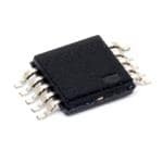
| 描述 | IC DAC 12BIT SERIAL IOUT 10-MSOP数模转换器- DAC 12-BIT IOUT w/ SERIAL ITF IC |
| 产品分类 | |
| 品牌 | Analog Devices |
| 产品手册 | |
| 产品图片 |
|
| rohs | 符合RoHS无铅 / 符合限制有害物质指令(RoHS)规范要求 |
| 产品系列 | 数据转换器IC,数模转换器- DAC,Analog Devices AD5443YRMZ- |
| 数据手册 | |
| 产品型号 | AD5443YRMZ |
| 产品培训模块 | http://www.digikey.cn/PTM/IndividualPTM.page?site=cn&lang=zhs&ptm=19145http://www.digikey.cn/PTM/IndividualPTM.page?site=cn&lang=zhs&ptm=18614http://www.digikey.cn/PTM/IndividualPTM.page?site=cn&lang=zhs&ptm=26125http://www.digikey.cn/PTM/IndividualPTM.page?site=cn&lang=zhs&ptm=26140http://www.digikey.cn/PTM/IndividualPTM.page?site=cn&lang=zhs&ptm=26150http://www.digikey.cn/PTM/IndividualPTM.page?site=cn&lang=zhs&ptm=26147 |
| 产品目录页面 | |
| 产品种类 | 数模转换器- DAC |
| 位数 | 12 |
| 供应商器件封装 | 10-MSOP |
| 分辨率 | 12 bit |
| 包装 | 管件 |
| 商标 | Analog Devices |
| 安装类型 | 表面贴装 |
| 安装风格 | SMD/SMT |
| 封装 | Tube |
| 封装/外壳 | 10-TFSOP,10-MSOP(0.118",3.00mm 宽) |
| 封装/箱体 | MSOP-10 |
| 工作温度 | -40°C ~ 125°C |
| 工厂包装数量 | 50 |
| 建立时间 | - |
| 接口类型 | SPI |
| 数据接口 | DSP,MICROWIRE™,QSPI™,串行,SPI™ |
| 最大功率耗散 | 25 uW |
| 最大工作温度 | + 125 C |
| 最小工作温度 | - 40 C |
| 标准包装 | 50 |
| 电压参考 | External |
| 电压源 | 单电源 |
| 电源电压-最大 | 5.5 V |
| 电源电压-最小 | 3 V |
| 稳定时间 | 90 ns |
| 系列 | AD5443 |
| 设计资源 | 点击此处下载产品Datasheet点击此处下载产品Datasheet点击此处下载产品Datasheet点击此处下载产品Datasheet点击此处下载产品Datasheet |
| 转换器数 | 1 |
| 转换器数量 | 1 |
| 输出数和类型 | 2 电流,单极2 电流,双极 |
| 配用 | /product-detail/zh/EV-AD5443%2F46%2F53SDZ/EV-AD5443%2F46%2F53SDZ-ND/4259593/product-detail/zh/EVAL-AD5443-DBRDZ/EVAL-AD5443-DBRDZ-ND/2027481 |
| 采样比 | 2.47 MSPs |
| 采样率(每秒) | 2.5M |


- 商务部:美国ITC正式对集成电路等产品启动337调查
- 曝三星4nm工艺存在良率问题 高通将骁龙8 Gen1或转产台积电
- 太阳诱电将投资9.5亿元在常州建新厂生产MLCC 预计2023年完工
- 英特尔发布欧洲新工厂建设计划 深化IDM 2.0 战略
- 台积电先进制程称霸业界 有大客户加持明年业绩稳了
- 达到5530亿美元!SIA预计今年全球半导体销售额将创下新高
- 英特尔拟将自动驾驶子公司Mobileye上市 估值或超500亿美元
- 三星加码芯片和SET,合并消费电子和移动部门,撤换高东真等 CEO
- 三星电子宣布重大人事变动 还合并消费电子和移动部门
- 海关总署:前11个月进口集成电路产品价值2.52万亿元 增长14.8%


PDF Datasheet 数据手册内容提取
8-/10-/12-Bit High Bandwidth Multiplying DACs with Serial Interface Data Sheet AD5426/AD5432/AD5443 FEATURES GENERAL DESCRIPTION 2.5 V to 5.5 V supply operation The AD5426/AD5432/AD54431 are CMOS 8-, 10-, and 12-bit 50 MHz serial interface current output digital-to-analog converters (DACs), respectively. 10 MHz multiplying bandwidth These devices operate from a 2.5 V to 5.5 V power supply, 2.5 MSPS update rate making them suitable for battery-powered applications and INL of ±1 LSB for 12-bit DAC many other applications. ±10 V reference input These DACs use a double buffered, 3-wire serial interface that is Low glitch energy < 2 nV-s compatible with SPI, QSPI™, MICROWIRE, and most DSP Extended temperature range −40°C to +125°C interface standards. In addition, a serial data out pin (SDO) 10-lead MSOP allows for daisy-chaining when multiple packages are used. Pin-compatible 8-, 10-, and 12-bit current output DACs Data readback allows the user to read the contents of the DAC Guaranteed monotonic register via the SDO pin. On power-up, the internal shift register 4-quadrant multiplication and latches are filled with 0s and the DAC outputs are at zero scale. Power-on reset with brownout detection Daisy-chain mode As a result of manufacturing on a CMOS submicron process, Readback function the parts offer excellent 4-quadrant multiplication characteristics 0.4 µA typical power consumption with large signal multiplying bandwidths of 10 MHz. The applied external reference input voltage, V , determines the full-scale APPLICATIONS REF output current. An integrated feedback resistor, R , provides FB Portable battery-powered applications temperature tracking and full-scale voltage output when combined Waveform generators with an external current to voltage precision amplifier. Analog processing The AD5426/AD5432/AD5443 DACs are available in small, Instrumentation 10-lead MSOPs. Programmable amplifiers and attenuators Digitally controlled calibration The EV-AD5443/46/53SDZ evaluation board is available for Programmable filters and oscillators evaluating DAC performance. For more information, see the Composite video UG-327 evaluation board user guide. Ultrasound Gain, offset, and voltage trimming FUNCTIONAL BLOCK DIAGRAM VDD VREF AD5426/ R RFB AD5432/ 8-/10-/12-BIT IOUT1 AD5443 R-2R DAC IOUT2 DAC REGISTER POWER-ON RESET INPUT LATCH SYNC CONTROL LOGIC AND SCLK INPUT SHIFT REGISTER SDIN SDO GND 03162-001 Figure 1. 1 Protected by U.S. Patent No. 5,689,257. Rev. H Document Feedback Information furnished by Analog Devices is believed to be accurate and reliable. However, no responsibility is assumed by Analog Devices for its use, nor for any infringements of patents or other One Technology Way, P.O. Box 9106, Norwood, MA 02062-9106, U.S.A. rights of third parties that may result from its use. Specifications subject to change without notice. No license is granted by implication or otherwise under any patent or patent rights of Analog Devices. Tel: 781.329.4700 ©2004–2015 Analog Devices, Inc. All rights reserved. Trademarks and registered trademarks are the property of their respective owners. Technical Support www.analog.com
AD5426/AD5432/AD5443 Data Sheet TABLE OF CONTENTS Features .............................................................................................. 1 Circuit Operation ....................................................................... 15 Applications ....................................................................................... 1 Single-Supply Applications ....................................................... 17 General Description ......................................................................... 1 Adding Gain ................................................................................ 17 Functional Block Diagram .............................................................. 1 DACs Used as a Divider or Programmable Gain Element ... 18 Revision History ............................................................................... 2 Reference Selection .................................................................... 18 Specifications ..................................................................................... 3 Amplifier Selection .................................................................... 18 Timing Characteristics ................................................................ 5 Serial Interface ............................................................................ 20 Absolute Maximum Ratings ............................................................ 6 PCB Layout and Power Supply Decoupling ................................ 22 ESD Caution .................................................................................. 6 Overview of the AD5426/AD5432/AD5443 and Related DACs .. 23 Pin Configuration and Function Descriptions ............................. 7 Outline Dimensions ....................................................................... 24 Typical Performance Characteristics ............................................. 8 Ordering Guide .......................................................................... 24 Terminology .................................................................................... 14 Theory of Operation ...................................................................... 15 REVISION HISTORY 9/15—Rev. G to Rev. H Deleted 80C51/80L51 to AD5426/AD5432/AD5443 Interface Deleted Positive Output Voltage Section and Figure 45; Section, Figure 55, MC68HC11 Interface to AD5426/AD5432/ Renumbered Sequentially .............................................................. 17 AD5443 Interface Section, Figure 56, MICROWIRE to Changes to Adding Gain Section ................................................. 17 AD5426/AD5432/AD5443 Interface Section, Figure 57, Changed Overview of AD54xx and AD55xx Devices Section PIC16C6x/7x to AD5426/AD5432/AD5443, and Figure 58 .... 22 to Overview of the AD5426/AD5432/AD5443 and Related Deleted Evaluation Board for the AD5426/AD5432/AD5443 DACs Section .................................................................................. 23 Series of DACs Section, Operating the Evaluation Board Changes to Ordering Guide .......................................................... 24 Section, and Power Supplies Section ........................................... 23 Deleted Figure 59 and Figure 60................................................... 24 6/13—Rev. F to Rev. G Updated Outline Dimensions ....................................................... 24 Change to General Description Section ........................................ 1 Changes to Ordering Guide .......................................................... 24 Changes to Ordering Guide .......................................................... 24 Deleted Figure 61 ............................................................................ 25 Deleted Figure 62 ............................................................................ 26 7/12—Rev. E to Rev. F No Change to Content, Changed V Values in 7/12 Revision 2/09—Rev. B to Rev. C DD History Only ...................................................................................... 2 Changes to Low Power Serial Interface Section and Daisy- Chain Mode Section ....................................................................... 20 7/12—Rev. D to Rev. E Updated Outline Dimensions ....................................................... 28 Changed V = 3 V to V = 2.5 V ............................. Throughout DD DD Changes to Table 2 ............................................................................ 4 11/08—Rev. A to Rev. B Changes to Table 4 ............................................................................ 7 Changes to Ordering Guide .......................................................... 28 Change to Daisy-Chain Mode Section ........................................ 20 Change to Ordering Guide ............................................................ 24 5/05—Rev. 0 to Rev. A Updated Format .................................................................. Universal 4/12—Rev. C to Rev. D Changes to Specifications ................................................................. 3 Changed V = 2.5 V to V = 3 V ............................. Throughout Changes to Figure 42 ...................................................................... 16 DD DD Changes to General Description Section ...................................... 1 Change to Figure 45 ....................................................................... 17 Deleted Microprocessor Interface Section, ADSP-21xx to Change to Figure 46 ....................................................................... 18 AD5426/AD5432/AD5443 Interface Section, Figure 51, Changes to Table 7, Table 8, and Table 9 ..................................... 19 Figure 52, Table 11, ADSP-BF5x to AD5426/AD5432/AD5443 Additions to Microprocessor Interface Section.......................... 21 Interface Section, Figure 53 and Figure 54; Renumbered Sequentially ..................................................................................... 21 2/04—Revision 0: Initial Version Rev. H | Page 2 of 24
Data Sheet AD5426/AD5432/AD5443 SPECIFICATIONS V = 2.5 V to 5.5 V, V = 10 V, I 2 = 0 V; temperature range for Y version: −40°C to +125°C; all specifications T to T , unless DD REF OUT MIN MAX otherwise noted; dc performance measured with OP177; ac performance with AD8038, unless otherwise noted. Table 1. Parameter Min Typ Max Unit Test Conditions/Comments STATIC PERFORMANCE AD5426 Resolution 8 Bits Relative Accuracy ±0.25 LSB Differential Nonlinearity ±0.5 LSB Guaranteed monotonic AD5432 Resolution 10 Bits Relative Accuracy ±0.5 LSB Differential Nonlinearity ±1 LSB Guaranteed monotonic AD5443 Resolution 12 Bits Relative Accuracy ±1 LSB Differential Nonlinearity −1/+2 LSB Guaranteed monotonic Gain Error ±10 mV Gain Error Temperature Coefficient1 ±5 ppm FSR/°C Output Leakage Current ±10 nA Data = 0x0000, T = 25°C, I 1 A OUT ±20 nA Data = 0x0000, T = −40°C to 125°C, I 1 OUT REFERENCE INPUT1 Reference Input Range ±10 V V Input Resistance 8 10 12 kΩ Input resistance TC = −50 ppm/°C REF R Resistance 8 10 12 kΩ Input resistance TC = −50 ppm/°C FB Input Capacitance Code Zero Scale 3 6 pF Code Full Scale 5 8 pF DIGITAL INPUT/OUTPUT1 Input High Voltage, V 1.7 V IH Input Low Voltage, V 0.6 V IL Output High Voltage, V V − 1 V V = 4.5 V to 5 V, I = 200 μA OH DD DD SOURCE V − 0.5 V V = 2.5 V to 3.6 V, I = 200 μA DD DD SOURCE Output Low Voltage, V 0.4 V V = 4.5 V to 5 V, I = 200 μA OL DD SINK 0.4 V V = 2.5 V to 3.6 V, I = 200 μA DD SINK Input Leakage Current, I 1 μA IL Input Capacitance 4 10 pF DYNAMIC PERFORMANCE1 Reference Multiplying Bandwidth 10 MHz V = ±3.5 V; DAC loaded all 1s REF Output Voltage Settling Time V = 10 V; R = 100 Ω, DAC latch alternately REF LOAD loaded with 0s and 1s Measured to ±16 mV of FS 50 100 ns Measured to ±4 mV of FS 55 110 ns Measured to ±1 mV of FS 90 160 ns Digital Delay 40 75 ns Interface delay time 10% to 90% Rise/Fall Time 15 30 ns Rise and fall time, V = 10 V, R = 100 Ω REF LOAD Digital-to-Analog Glitch Impulse 2 nV-s 1 LSB change around major carry, V = 0 V REF Multiplying Feedthrough Error DAC latch loaded with all 0s, V = ±3.5 REF 70 dB 1 MHz 48 dB 10 MHz Rev. H | Page 3 of 24
AD5426/AD5432/AD5443 Data Sheet Parameter Min Typ Max Unit Test Conditions/Comments Output Capacitance I 1 12 17 pF All 0s loaded OUT 10 12 pF All 1s loaded I 2 22 25 pF All 0s loaded OUT 10 12 pF All 1s loaded Digital Feedthrough 0.1 nV-s Feedthrough to DAC output with SYNC high and alternate loading of all 0s and all 1s Analog THD 81 dB V = 3.5 V p-p, all 1s loaded, f = 1 kHz REF Digital THD Clock = 1 MHz, V = 3.5 V, C = 1.8 pF REF COMP 50 kHz f 73 dB OUT 20 kHz f 74 dB OUT Output Noise Spectral Density 25 nV/√Hz @ 1 kHz SFDR Performance (Wide Band) Clock = 1 MHz, V = 3.5 V REF 50 kHz f 75 dB OUT 20 kHz f 76 dB OUT SFDR Performance (Narrow Band) Clock = 1 MHz, V = 3.5 V REF 50 kHz f 87 dB OUT 20 kHz f 87 dB OUT Intermodulation Distortion 78 dB Clock = 1 MHz, f = 20 kHz, f = 25 kHz, V = 3.5 V 1 2 REF POWER REQUIREMENTS Power Supply Range 2.5 5.5 V I 0.6 µA T = 25°C, logic inputs = 0 V or V DD A DD 0.4 5 µA T = −40°C to +125°C , logic inputs = 0 V or V DD Power Supply Sensitivity1 0.001 %/% ∆V = ±5% DD 1 Guaranteed by design and characterization, not subject to production testing. Rev. H | Page 4 of 24
Data Sheet AD5426/AD5432/AD5443 TIMING CHARACTERISTICS All input signals are specified with tr = tf = 1 ns (10% to 90% of V ) and timed from a voltage level of (V + V )/2. V = 2.5 V to 5.5 V, DD IL IH DD V = 10 V, I 2 = 0 V; temperature range for Y version: −40°C to +125°C; all specifications T to T , unless otherwise noted. REF OUT MIN MAX Table 2. Parameter 2.5 V to 5.5 V 4.5 V to 5.5 V Unit Test Conditions/Comments f 50 50 MHz max Max clock frequency SCLK t 20 20 ns min SCLK cycle time 1 t 8 8 ns min SCLK high time 2 t 8 8 ns min SCLK low time 3 t41 13 13 ns min SYNC falling edge to SCLK active edge setup time t 5 5 ns min Data setup time 5 t 3 3 ns min Data hold time 6 t7 5 5 ns min SYNC rising edge to SCLK active edge t8 30 30 ns min Minimum SYNC high time t 2, 3 80 45 ns typ SCLK active edge to SDO valid 9 120 65 ns max 1 Falling or rising edge as determined by control bits of serial word. 2 Daisy-chain and readback modes cannot operate at maximum clock frequency. SDO timing specifications measured with load circuit, as shown in Figure 4. 3 SDO operates with a VDD of 3.0 V to 5.5 V. t1 SCLK t2 t3 t8 t4 t7 SYNC t6 t5 DIN DB15 DB0 ASCLTLEKR ANSA DTIEVTEELRYM, DINAETDA B MYA CYO BNET CRLOOLC BKITESD. ITNIMTOIN IGN PAUST P SEHRI FATB ROEVGEI,S WTEITRH OSNC LRKIS IINNVGE ERDTGEDE. OF 03162-002 Figure 2. Standalone Mode Timing Diagram t1 SCLK t2 t3 t7 t4 t8 t6 SYNC t6 t5 DB15� DB0 SDIN DB15 (N) DB0 (N) (N + 1) (N + 1) t9 SDO DB15(N) DB0(N) ADEDLETTGEEERR ONMFAIN TSEICVDLE KBL.YY T, CIDMOAINNTTGAR AMOSAL Y PB EBITRES AC. BILNOO TVCHEKI,SE W DCI ATINHST ESO,C DILNAKPT UIANT VW SEOHRUITFLETD DR .BEEG ICSLTOECRK OEND ROIUSITN OGF E SDDGOE OONF FSACLLLKI NAGS 03162-003 Figure 3. Daisy-Chain and Readback Modes Timing Diagram Rev. H | Page 5 of 24
AD5426/AD5432/AD5443 Data Sheet ABSOLUTE MAXIMUM RATINGS Transient currents of up to 100 mA do not cause SCR latch-up. Stresses at or above those listed under Absolute Maximum T = 25°C, unless otherwise noted. A Ratings may cause permanent damage to the product. This is a stress rating only; functional operation of the product at these Table 3. or any other conditions above those indicated in the operational Parameter Rating section of this specification is not implied. Operation beyond V to GND −0.3 V to +7 V DD the maximum operating conditions for extended periods may V , R to GND −12 V to +12 V REF FB affect product reliability. I 1, I 2 to GND −0.3 V to V + 0.3 V OUT OUT DD Logic Inputs and Output1 −0.3 V to V + 0.3 V DD 200µA IOL Operating Temperature Range Extended Industrial (Y Version) −40°C to +125°C Storage Temperature Range −65°C to +150°C TO OUTPUT PIN VOH (MIN) + VOL (MAX) Junction Temperature 150°C 20CpFL 2 1Le0a-lde aTdem MpSeOrPat θuJrAe T, hSeorldmearli nImg p(1e0d saencc)e 230060°°CC/ W 200µA IOH 03162-004 IR Reflow, Peak Temperature (<20 sec) 235°C Figure 4. Load Circuit for SDO Timing Specifications 1 Overvoltages at SCLK, SYNC, and DIN are clamped by internal diodes. ESD CAUTION Rev. H | Page 6 of 24
Data Sheet AD5426/AD5432/AD5443 PIN CONFIGURATION AND FUNCTION DESCRIPTIONS IOUT1 1 10 RFB AD5426/ IOUT2 2 AD5432/ 9 VREF GND 3 AD5443 8 VDD SSCDLIKN 45 (NToOt Pto V SIEcaWle) 76 SSDYNOC 03162-005 Figure 5. Pin Configuration Table 4. Pin Function Descriptions Pin No. Mnemonic Description 1 I 1 DAC Current Output. OUT 2 I 2 DAC Analog Ground. This pin should normally be tied to the analog ground of the system. OUT 3 GND Digital Ground Pin. 4 SCLK Serial Clock Input. By default, data is clocked into the input shift register on the falling edge of the serial clock input. Alternatively, by means of the serial control bits, the device may be configured such that data is clocked into the shift register on the rising edge of SCLK. The device can accommodate clock rates up to 50 MHz. 5 SDIN Serial Data Input. Data is clocked into the 16-bit input register on the active edge of the serial clock input. By default, on power-up, data is clocked into the shift register on the falling edge of SCLK. The control bits allow the user to change the active edge to rising edge. 6 SYNC Active Low Control Input. This is the frame synchronization signal for the input data. When SYNC goes low, it powers on the SCLK and DIN buffers, and the input shift register is enabled. Data is loaded to the mode, the serial interface counts clocks, and data is latched to the shift register on the 16th active clock edge. 7 SDO Serial Data Output. This allows a number of parts to be daisy-chained. By default, data is clocked into the shift register on the falling edge and out via SDO on the rising edge of SCLK. Data is always clocked out on the alternate edge to loading data to the shift register. Writing the readback control word to the shift register makes the DAC register contents available for readback on the SDO pin, clocked out on the opposite edges to the active clock edge. SDO operates with a V of 3.0 V to 5.5 V. DD 8 V Positive Power Supply Input. These parts can be operated from a supply of 2.5 V to 5.5 V. DD 9 V DAC Reference Voltage Input. REF 10 R DAC Feedback Resistor Pin. Establish voltage output for the DAC by connecting to external amplifier output. FB Rev. H | Page 7 of 24
AD5426/AD5432/AD5443 Data Sheet TYPICAL PERFORMANCE CHARACTERISTICS 0.20 0.20 TA = 25°C TA = 25°C VREF = 10V VREF = 10V 0.15 VDD = 5V 0.15 VDD = 5V 0.10 0.10 0.05 0.05 B) B) LS 0 LS 0 L ( L ( N N I–0.05 I–0.05 –0.10 –0.10 –0.15 –0.15 –0.200 50 100 CODE150 200 250 03162-006 –0.200 50 100 CODE150 200 250 03162-009 Figure 6. INL vs. Code (8-Bit DAC) Figure 9. DNL vs. Code (8-Bit DAC) 0.5 0.5 TA = 25°C TA = 25°C 0.4 VREF = 10V 0.4 VREF = 10V VDD = 5V VDD = 5V 0.3 0.3 0.2 0.2 0.1 0.1 iNL (LSB) –0.01 DNL (LSB) –0.01 –0.2 –0.2 –0.3 –0.3 –0.4 –0.4 –0.50 200 400 CODE600 800 10000 03162-007 –0.50 200 400 CODE600 800 1000 03162-010 Figure 7. INL vs. Code (10-Bit DAC) Figure 10. DNL vs. Code (10-Bit DAC) 1.0 1.0 TA = 25°C TA = 25°C 0.8 VREF = 10V 0.8 VREF = 10V VDD = 5V VDD = 5V 0.6 0.6 0.4 0.4 0.2 0.2 INL (LSB) –0.02 DNL (LSB) –0.02 –0.4 –0.4 –0.6 –0.6 –0.8 –0.8 –1.00 500 1000 1500 2C0O0D0E 2500 3000 3500 4000 03162-008 –1.00 500 1000 1500 2C0O0D0E 2500 3000 3500 4000 03162-011 Figure 8. INL vs. Code (12-Bit DAC) Figure 11. DNL vs. Code (12-Bit DAC) Rev. H | Page 8 of 24
Data Sheet AD5426/AD5432/AD5443 0.6 2.0 0.5 1.5 0.4 MAX INL MAX INL 1.0 0.3 TA = 25°C 0.5 VREF = 0V VDD = 3V B) 0.2 AD5443 NL (LS 0.1 AVTADD D5= 4 =24 553°VC LSB 0 MAX DNL I –0.5 0 –1.0 MIN INL –0.1 MIN INL MIN DNL –0.2 –1.5 –0.32 3 4 REF5ERENC6E VOLT7AGE 8 9 10 03162-012 –2.00.5 0.6 0.7 0.8 0.9VBI1A.S0 (V)1.1 1.2 1.3 1.4 1.5 03162-015 Figure 12. INL vs. Reference Voltage Figure 15. Linearity vs. VBIAS Voltage Applied to IOUT2 –0.40 4 VTAD D= =2 55°VC 3 TVAR E=F 2=5 °2C.5V MAX DNL –0.45 AD5443 VDD = 3V AD5443 2 MAX INL –0.50 1 B) 0 S L–0.55 B NL ( LS –1 MIN DNL D –0.60 –2 MIN INL MIN DNL –3 –0.65 –4 –0.702 3 4 REF5ERENC6E VOLT7AGE 8 9 10 03162-013 –50 0.2 0.4 0.6 0.8VBI1A.S0 (V)1.2 1.4 1.6 1.8 2.0 03162-016 Figure 13. DNL vs. Reference Voltage Figure 16. Linearity vs. VBIAS Voltage Applied to IOUT2 5 0.5 VREF = 10V TA = 25°C 4 0.4 VREF = 0V VDD = 3V AND 5V 3 0.3 2 VDD = 5V 0.2 OR (mV) 10 VDD = 3V AGE (mV) 0.10 GAIN ERROR OFFSET ERROR RR –1 LT –0.1 E O V –2 –0.2 –3 –0.3 –4 –0.4 –5–60 –40 –20 0 TE2M0PERA40TURE6 0(°C) 80 100 120 140 03162-014 –0.50.5 0.6 0.7 0.8 0.9VBI1A.S0 (V)1.1 1.2 1.3 1.4 1.5 03162-017 Figure 14. Gain Error vs. Temperature Figure 17. Gain and Offset Errors vs. VBIAS Voltage Applied to IOUT2 Rev. H | Page 9 of 24
AD5426/AD5432/AD5443 Data Sheet 0.5 0.7 TA = 25°C TA = 25°C 0.4 VREF = 2.5V VDD = 3V AND 5V 0.6 0.3 GAIN ERROR 0.2 0.5 VDD = 5V V) 0.1 A) m m 0.4 GE ( 0 OFFSET ERROR NT ( A E LT –0.1 RR 0.3 O U V C –0.2 0.2 –0.3 0.1 –0.4 VDD = 3V –0.50 0.2 0.4 0.6 0.8VBI1A.S0 (V)1.2 1.4 1.6 1.8 2.0 03162-018 00 1 INP2UT VOLTAGE3 (V) 4 5 03162-021 Figure 18. Gain and Offset Errors vs. VBIAS Voltage Applied to IOUT2 Figure 21. Supply Current vs. Logic Input Voltage, SYNC (SCLK), DATA = 0 3 1.6 TA = 25°C VREF = 0V 2 VADDD5 4=4 53V MAX INL 1.4 1.2 1 nA) 1.0 IOUT1 VDD 5V MAX DNL GE ( B 0 A 0.8 S K L A E –1 LUT 0.6 MIN INL IO 0.4 IOUT1 VDD 3V –2 MIN DNL 0.2 –30.5 1.0 VBI1A.S5 (V) 2.0 2.5 03162-019 0–40 –20 0 T2E0MPER4A0TURE6 (0°C) 80 100 120 03162-022 Figure 19. Linearity vs. VBIAS Voltage Applied to IOUT2 Figure 22. IOUT1 Leakage Current vs. Temperature 4 0.50 TA = 25°C 3 VREF = 2.5V 0.45 VDD = 5V AD5443 0.40 2 VDD = 5V MAX DNL 0.35 1 ALL 0s A) 0.30 B 0 MAX INL µNT ( 0.25 ALL 1s LS –1 MIN DNL RE R 0.20 U –2 C VDD = 3V 0.15 –3 0.10 ALL 1s ALL 0s –4 MIN INL 0.05 –50.5 1.0 VBIAS (V) 1.5 2.0 03162-020 0–60 –40 –20 0 TE2M0PERA40TURE6 0(°C) 80 100 120 140 03162-023 Figure 20. Linearity vs. VBIAS Voltage Applied to IOUT2 Figure 23. Supply Current vs. Temperature Rev. H | Page 10 of 24
Data Sheet AD5426/AD5432/AD5443 3.5 3 ATAD 5=4 2453°C VREF =±0.15V, AD8038 CC 1pF 3.0 LOADING 010101010101 VREF =±2V, AD8038 CC 1pF 0 2.5 VREF =±3.51V, AD8038 CC 1.8pF I (mA)DD 21..05 VCC = 5V GAIN (dB) –3 VREVFR =EF± =0.1±52VV,, AADD88003388 CCCC 11..4477ppFF 1 –6 0.5 VCC = 3V TA = 25°C VDD = 5V AD8038 AMPLIFIER 01 10 100 1FkREQU1E0NkCY (1H0z0)k 1M 10M 100M 03162-024 –910k 100k FREQUE1MNCY (Hz) 10M 100M 03162-027 Figure 24. Supply Current vs. Update Rate Figure 27. Reference Multiplying Bandwidth vs. Frequency and Compensation Capacitor 6 0.060 0 LOADING ALL ON VDD 5V, 0V REF TA = 25°C –––11628 ZS TO FS DDDBBB11910 0.050 N0xR7GF F= T2O.0 409xn8V00s VACARDDCEO85FM04 34=P83 0= AV 1M.8PpLFIFIER –24 DB8 0.040 GAIN (dB) –––––––33445660628406 DDDDDDDBBBBBBB7654321 TPUT VOLTAGE (V)000...000312000 VN0xDR8DG0 3 0=V VN0T 0,xD OR.070DG VF08 3 Fx8R=V7 n TE1,FV OF.0Fs8V 70 7xRn8EV0F0s –72 DB0 OU 0 –78 TA = 25°C –––899406 ALL OFF CCVORMEPFV D==D 1± =3.8 .55pVVF –0.010 VN0xDR8DG0 5 0=V T 0, O.01 V01 x9R7nEFVFFs, AD8038 AMPLIFIER –1021 10 100 1FkREQU1E0NkCY (1H0z0)k 1M 10M 100M 03162-025 –0.0200 50 100 TIM1E5 0(ns) 200 250 300 03162-028 Figure 25. Reference Multiplying Bandwidth vs. Frequency and Code Figure 28. Midscale Transition VREF = 0 V 0.2 –1.70 VDD 5V, 3.5V REF TA = 25°C NRG = 1.184nVs VREF = 3.5V 0x7FF TO 0x800 AD8038 AMPLIFIER 0 –1.71 CCOMP = 1.8pF AD5443 GAIN (dB) ––00..24 UTPUT VOLTAGE (V)–––111...777234 VN0xDR7DGVNF D3R F=VDG T 1,3 O.3=V4. 350,0 3V.3x6n.8 45RV07VE0sn FRVEsF O 0x800 TO 0x7FF –0.6 TA = 25°C VDD = 5V –1.75 VREF =±3.5V CCOMP = 1.8pF VDD 5V, 3.5V REF, NRG = 0.364nVs, AD8038 AMPLIFIER 0x800 TO 0x7FF –0.81 10 100 1FkREQU1E0NkCY (1H0z0)k 1M 10M 100M 03162-026 –1.760 50 100 TIM1E5 0(ns) 200 250 300 03162-029 Figure 26. Reference Multiplying Bandwidth—All 1s Loaded Figure 29. Midscale Transition VREF = 3.5 V Rev. H | Page 11 of 24
AD5426/AD5432/AD5443 Data Sheet 20 100 TA = 25°C VDD = 3V 0 AMPLIFIER = AD8038 MCLK = 200kHz 80 –20 MCLK = 500kHz MCLK = 1MHz 60 B) –40 B) d d R ( R ( R –60 D PS FULL SCALE SF 40 –80 ZERO SCALE 20 –100 TA = 25°C VREF = 3.5V AD8038 AMP AD5443 –1201 10 100 FRE1QkUENC1Y0 (kHz) 100k 1M 10M 03162-030 00 10 20fOUT (kHz)30 40 50 03162-034 Figure 30. Power Supply Rejection vs. Frequency Figure 33. Wideband SFDR vs. fOUT Frequency (AD5443) –60 80 TVAD D= =2 53°VC MCLK = 500kHz –65 VREF = 3.5V p-p 60 MCLK = 1MHz MCLK = 200kHz –70 B) + N (d –75 R (dB) 40 THD –80 SFD 20 –85 TA = 25°C VREF = 3.5V AD8038 AMP –901 10 100FREQUE1NkCY (Hz)10k 100k 1M 03162-031 00AD5426 10 20fOUT (kHz)30 40 50 03162-035 Figure 31. THD and Noise vs. Frequency Figure 34. Wideband SFDR vs. fOUT Frequency (AD5426) 1.8 TA = 25°C –100 TVAR E=F 2=5 3°C.5V 1.6 AD8038 AMPLIFIER AD5443 –20 1.4 V) VIH –30 E ( 1.2 G –40 VOLTA 1.0 VIL R (dB) –50 D 0.8 D OL SF –60 H S 0.6 –70 E R TH 0.4 –80 0.2 –90 02.5 3.0 3.5 VOLT4A.0GE (V) 4.5 5.0 5.5 03162-033 –1000 50 100 150 F2R0E0QU2E5N0CY 3(H00z) 350 400 450 500 03162-036 Figure 32. Threshold Voltages vs. Supply Voltage Figure 35. Wideband SFDR fOUT = 50 kHz, Update = 1 MHz Rev. H | Page 12 of 24
Data Sheet AD5426/AD5432/AD5443 0 0 TA = 25°C TA = 25°C –10 VREF = 3.5V –10 VREF = 3.5V AD8038 AMPLIFIER AD8038 AMPLIFIER AD5443 AD5443 –20 –20 –30 –30 –40 –40 B) B) R (d –50 R (d –50 D D F –60 F –60 S S –70 –70 –80 –80 –90 –90 –1000 50 100 150 F2R0E0QU2E5N0CY 3(H00z) 350 400 450 500 03162-037 –10010 12 14 16 FR18EQUE2N0CY (2H2z) 24 26 28 30 03162-039 Figure 36. Wideband SFDR fOUT = 20 kHz, Update = 1 MHz Figure 38. Narrowband (±50%) SFDR fOUT = 20 kHz, Update = 1 MHz –100 TVAARD E8=F0 23=58 °3 CA.5MVPLIFIER –100 TVAARD E8=F0 23=58 °3 CA.5MVPLIFIER –20 AD5443 –20 AD5443 –30 –30 –40 –40 B) R (d –50 B –50 D d SF –60 –60 –70 –70 –80 –80 –90 –90 –10025 30 35 40 FR45EQUE5N0CY (5H5z) 60 65 70 75 03162-038 –10010 15 FR20EQUENCY (2H5z) 30 35 03162-040 Figure 37. Narrowband (±50%) SFDR fOUT = 50 kHz, Update = 1 MHz Figure 39. Narrowband (±50%) IMD fOUT = 20 kHz, 25 kHz, Update = 1 MHz Rev. H | Page 13 of 24
AD5426/AD5432/AD5443 Data Sheet TERMINOLOGY Relative Accuracy Digital Feedthrough Relative accuracy or endpoint nonlinearity is a measure of the When the device is not selected, high frequency logic activity maximum deviation from a straight line passing through the on the device digital inputs may be capacitively coupled to show endpoints of the DAC transfer function. It is measured after up as noise on the I pins and subsequently into the following OUT adjusting for 0 and full scale and is normally expressed in LSBs circuitry. This noise is digital feedthrough. or as a percentage of full-scale reading. Multiplying Feedthrough Error Differential Nonlinearity This is the error due to capacitive feedthrough from the DAC Differential nonlinearity is the difference between the measured reference input to the DAC I 1 terminal, when all 0s are OUT change and the ideal 1 LSB change between any two adjacent loaded to the DAC. codes. A specified differential nonlinearity of −1 LSB maximum Total Harmonic Distortion (THD) over the operating temperature range ensures monotonicity. The DAC is driven by an ac reference. The ratio of the rms sum Gain Error of the harmonics of the DAC output to the fundamental value is Gain error or full-scale error is a measure of the output error the THD. Usually only the lower order harmonics are included, between an ideal DAC and the actual device output. For these such as second to fifth. DACs, ideal maximum output is VREF − 1 LSB. Gain error of the ( ) V 2 +V 2 +V 2 +V 2 DACs is adjustable to 0 with external resistance. THD=20log 2 3 4 5 V Output Leakage Current 1 Output leakage current is current that flows in the DAC ladder Digital Intermodulation Distortion switches when these are turned off. For the IOUT1 terminal, it Second-order intermodulation distortion (IMD) measurements can be measured by loading all 0s to the DAC and measuring are the relative magnitude of the fa and fb tones generated the IOUT1 current. Minimum current flows in the IOUT2 line digitally by the DAC and the second-order products at 2fa − fb when the DAC is loaded with all 1s. and 2fb − fa. Output Capacitance Spurious-Free Dynamic Range (SFDR) Capacitance from IOUT1 or IOUT2 to AGND. SFDR is the usable dynamic range of a DAC before spurious noise interferes or distorts the fundamental signal. It is the mea- Output Current Settling Time sure of the difference in amplitude between the fundamental This is the amount of time it takes for the output to settle to a and the largest harmonically or nonharmonically related spur specified level for a full-scale input change. For these devices, it from dc to full Nyquist bandwidth (half the DAC sampling rate, is specified with a 100 Ω resistor to ground. or f/2). Narrow band SFDR is a measure of SFDR over an S The settling time specification includes the digital delay from arbitrary window size, in this case 50% of the fundamental. SYNC rising edge to the full-scale output charge. Digital SFDR is a measure of the usable dynamic range of the Digital-to-Analog Glitch Impulse DAC when the signal is a digitally generated sine wave. The amount of charge injected from the digital inputs to the analog output when the inputs change state. This is normally specified as the area of the glitch in either pA-s or nV-s depending upon whether the glitch is measured as a current or voltage signal. Rev. H | Page 14 of 24
Data Sheet AD5426/AD5432/AD5443 THEORY OF OPERATION The AD5426, AD5432, and AD5443 are 8-, 10-, and 12-bit Note that the output voltage polarity is opposite to the V REF current output DACs consisting of a standard inverting R-2R polarity for dc reference voltages. ladder configuration. A simplified diagram for the 8-bit AD5426 is These DACs are designed to operate with either negative or shown in Figure 40. The matching feedback resistor, R , has a FB positive reference voltages. The V power pin is used by only the DD value of R. The value of R is typically 10 kΩ (minimum 8 kΩ internal digital logic to drive the DAC switches’ on and off states. and maximum 12 kΩ). If I 1 and I 2 are kept at the same OUT OUT These DACs are also designed to accommodate ac reference potential, a constant current flows in each ladder leg, regardless input signals in the range of −10 V to +10 V. of digital input code. Therefore, the input resistance presented at V is always constant and nominally of value R. The DAC With a fixed 10 V reference, the circuit shown in Figure 41 gives REF output (IOUT) is code-dependent, producing various resistances a unipolar 0 V to −10 V output voltage swing. When VIN is an ac and capacitances. External amplifier choice should take into signal, the circuit performs 2-quadrant multiplication. Table 5 account the variation in impedance generated by the DAC on shows the relationship between digital code and expected output the amplifiers inverting input node. voltage for unipolar operation (AD5426, 8-bit device). R R R VREF Table 5. Unipolar Code Table 2R 2R 2R 2R 2R Digital Input Analog Output (V) S1 S2 S3 S8 R RFBA 1111 1111 −VREF (255/256) IOUT1 1000 0000 −VREF (128/256) = −VREF/2 IOUT2 0000 0001 −V (1/256) DACA N DDA DTAR ILVAETRCSHES 03162-041 0000 0000 −VRREEFF (0/256) = 0 Figure 40. Simplified Ladder VDD R2 Access is provided to the V , R , I 1, and I 2 terminals of REF FB OUT OUT the DAC, making the device extremely versatile and allowing it C1 to be configured in several different operating modes. For example, VDD RFB it can be configured to provide a unipolar output, 4-quadrant VREF VREF AADD55442362// IOUT1 AA11 multiplication in bipolar or single-supply modes of operation. R1 AD5443 IOUT2 VOUT = 0 SYNCSCLK SDIN GND TO–VREF Note that a matching switch is used in series with the internal R feedback resistor. If users attempt to measure R , power FB FB must be applied to V to achieve continuity. MICROCONTROLLER AGND DD CIRCUIT OPERATION NOTES Unipolar Mode 12..RCIF11 A AP1HN IADSS ARE 2H CUIGOSHME DPSE PONENSELADYT AIIFOM NGP AL(1IIFNpIF EA RTDO.J U2SpFT)M MEANYT BISE R REEQQUUIRIREEDD. 03162-042 Using a single op amp, these devices can easily be configured to Figure 41. Unipolar Operation provide 2-quadrant multiplying operation or a unipolar output voltage swing, as shown in Figure 41. When an output amplifier is connected in unipolar mode, the output voltage is given by D V =−V × OUT REF 2n where D is the fractional representation of the digital word loaded to the DAC, and n is the number of bits. D = 0 to 255 (8-bit AD5426) = 0 to 1023 (10-bit AD5432) = 0 to 4095 (12-bit AD5443) Rev. H | Page 15 of 24
AD5426/AD5432/AD5443 Data Sheet Bipolar Operation Table 6. Bipolar Code Table Digital Input Analog Output (V) In some applications, it may be necessary to generate full 4-quadrant multiplying operation or a bipolar output swing. 1111 1111 +VREF (127/128) This can easily be accomplished by using another external 1000 0000 0 amplifier and some external resistors, as shown in Figure 42. 0000 0001 −VREF (127/128) In this circuit, the second amplifier, A2, provides a gain of 2. 0000 0000 −VREF (128/128) Biasing the external amplifier with an offset from the reference Stability voltage results in full 4-quadrant multiplying operation. The In the I-to-V configuration, the I of the DAC and the inverting OUT transfer function of this circuit shows that both negative and node of the op amp must be connected as close as possible and positive output voltages are created as the input data, D, which proper PCB layout techniques must be employed. Since every is incremented from code zero (V = −V ) to midscale OUT REF code change corresponds to a step function, gain peaking may (V = 0 V) to full scale (V = +V ). OUT OUT REF occur if the op amp has limited gain bandwidth product (GBP) D and there is excessive parasitic capacitance at the inverting node. V =V × −V OUT REF 2n−1 REF This parasitic capacitance introduces a pole into the open-loop response that can cause ringing or instability in closed-loop where D is the fractional representation of the digital word applications. loaded to the DAC and n is the resolution of the DAC. An optional compensation capacitor, C1, can be added in parallel D = 0 to 255 (8-bit AD5426) with R for stability, as shown in Figure 41 and Figure 42. Too = 0 to 1023 (10-bit AD5432) FB small a value of C1 can produce ringing at the output, while = 0 to 4095 (12-bit AD5443) too large a value can adversely affect the settling time. C1 should When V is an ac signal, the circuit performs 4-quadrant IN be found empirically, but 1 pF to 2 pF is generally adequate for multiplication. compensation. Table 6 shows the relationship between digital code and the expected output voltage for bipolar operation (AD5426, 8-bit device). R3 20kΩ R5 VDD R2 20kΩ C1 VDD RFB R4 AD5426/ IOUT1 10kΩ V±R1E0VF R1 VREF AADD55443423/ IOUT2 AA11 A2 SYNCSCLK SDIN GND VOUT =–VREF TO +VREF MICROCONTROLLER AGND NOTES 1.R1 AND R2 ARE USED ONLY IF GAIN ADJUSTMENT IS REQUIRED. ADJUST R1 FOR VOUT = 0V WITH CODE 10000000 LOADED TO DAC. 23..MCSP1A ETPECHDHA ISANEMG PC ALONIMFDIPE TERRN.ASCAKTIINOGN I(S1 pEFS TSOE N2TpIFA)L M FAOYR B REE RSEISQTUOIRRE PDA IIFR SA 1R/3A 2A NISD A R H4I.GH 03162-043 Figure 42. Bipolar Operation Rev. H | Page 16 of 24
Data Sheet AD5426/AD5432/AD5443 SINGLE-SUPPLY APPLICATIONS VDD R1 R2 Current Mode Operation These DACs are specified and tested to guarantee operation in RFB VDD A1 VOUT single-supply applications. In the current mode circuit of Figure 43, VIN IOUT1 VREF I 2 and hence I 1 is biased positive by an amount applied to OUT OUT GND V . BIAS VDD NOTES VDD RFB C1 12..ACIFD1 A DP1IHT IASIOS ANE AH CLIGO PHMIN PSSEP NOESEMADITT ATIOMENDP L(F1IOFpIRFE RTCO.L A2RpFIT)Y M.AY BE REQUIRED 03162-045 IOUT1 VIN VREF AA11 VOUT Figure 44. Single-Supply Voltage Switching Mode Operation IOUT2 GND It is important to note that V is limited to low voltages because IN the switches in the DAC ladder no longer have the same source drain drive voltage. As a result, their on resistance differs, which degrades the linearity of the DAC. A2 VBIAS Also, VIN must not go negative by more than 0.3 V or an NOTES internal diode turns on, exceeding the maximum ratings of the 12..ACRD1E QDPIUHTIAIROSENEDA CLIFO P AMIN1P SEIS NO ASM AHITTIGTIOEHND S (FP1OpERFE DTC OLA AM2RpPFILT)IY FM.IEARY. BE 03162-044 dcaepvaicbei.l iItny othf itsh tey pDeA oCf aisp plolisct.a tion, the full range of multiplying Figure 43. Single-Supply Current Mode Operation ADDING GAIN In this configuration, the output voltage is given by In applications where the output voltage is required to be greater VOUT = {D × (RFB/RDAC) × (VBIAS − VIN)} + VBIAS than VIN, gain can be added with an additional external amplifier or it can be achieved in a single stage. It is important to consider the As D varies from 0 to 255 (AD5426), 1023 (AD5432) or 4095 effect of temperature coefficients of the thin film resistors of the (AD5443), the output voltage varies from DAC. Simply placing a resistor in series with the R resistor causes FB VOUT = VBIAS to VOUT = 2 VBIAS − VIN mismatches in the temperature coefficients, resulting in larger V should be a low impedance source capable of sinking and gain temperature coefficient errors. Instead, the circuit shown BIAS sourcing all possible variations in current at the I 2 terminal in Figure 45 is a recommended method of increasing the gain of OUT without any problems. the circuit. R1, R2, and R3 should all have similar temperature coefficients, but they need not match the temperature coefficients It is important to note that V is limited to low voltages because IN of the DAC. This approach is recommended in circuits where the switches in the DAC ladder no longer have the same source gains of greater than 1 are required. drain drive voltage. As a result, their on resistance differs, which degrades the linearity of the DAC. See Figure 15 to Figure 20. Note that RFB is much greater than R2||R3 and that a gain error percentage of 100 × (R2||R3)/R must be taken into consideration. Voltage Switching Mode of Operation FB VDD Figure 44 shows these DACs operating in the voltage switching mode. The reference voltage, V , is applied to the I 1 pin, IN OUT C1 IOUT2 is connected to AGND, and the output voltage is available VDD RFB at the VREF terminal. In this configuration, a positive reference VIN R1 VREF IOUT1 A1 VOUT voltage results in a positive output voltage, making single-supply IOUT2 R3 operation possible. The output from the DAC is voltage at a GND GAIN = R2 + R3 constant impedance (the DAC ladder resistance), thus an op R2 R2 amp is necessary to buffer the output voltage. The reference R1 = R2R3 input no longer sees a constant input impedance, but one that NOTES R2 + R3 vfraormies a w loitwh icmodpee.d Tanhecere sfoourer,c teh. e voltage input should be driven 12..ACIFD1 A DP1IHT IASIOS ANE AH CLIGO PHMIN PSSEP NOESEMADITT ATIOMENDP L(F1IOFpIRFE RTCO.L A2RpFIT)Y M.AY BE REQUIRED 03162-047 Figure 45. Increasing Gain of Current Output DAC Rev. H | Page 17 of 24
AD5426/AD5432/AD5443 Data Sheet DACS USED AS A DIVIDER OR PROGRAMMABLE REFERENCE SELECTION GAIN ELEMENT When selecting a reference for use with the AD5426 series of Current-steering DACs are very flexible and lend themselves to current output DACs, pay attention to the references output many different applications. If this type of DAC is connected as voltage temperature coefficient specification. This parameter not the feedback element of an op amp and R is used as the input only affects the full-scale error, but can also affect the linearity (INL FB resistor as shown in Figure 46, then the output voltage is inversely and DNL) performance. The reference temperature coefficient proportional to the digital input fraction, D. should be consistent with the system accuracy specifications. For example, an 8-bit system required to hold its overall specification to For D = 1 − 2−n the output voltage is within 1 LSB over the temperature range 0°C to 50°C dictates V = −V /D = −V /(1 − 2−N) OUT IN IN that the maximum system drift with temperature should be less As D is reduced, the output voltage increases. For small values of than 78 ppm/°C. A 12-bit system with the same temperature D, it is important to ensure that the amplifier does not saturate and range to overall specification within 2 LSBs requires a maximum also that the required accuracy is met. For example, an 8-bit DAC drift of 10 ppm/°C. By choosing a precision reference with low driven with the binary code 0x10 (00010000), that is, 16 decimal, in output temperature coefficient this error source can be minimized. the circuit of Figure 46 should cause the output voltage to be 16 Table 7 suggests some references available from Analog Devices × V . However, if the DAC has a linearity specification of ±0.5 IN that are suitable for use with this range of current output DACs. LSB, then D can in fact have the weight anywhere in the range AMPLIFIER SELECTION 15.5/256 to 16.5/256 so that the possible output voltage will be in the range 15.5 V to 16.5 V —an error of +3% even though the The primary requirement for the current-steering mode is an IN IN DAC itself has a maximum error of 0.2%. amplifier with low input bias currents and low input offset voltage. The input offset voltage of an op amp is multiplied by DAC leakage current is also a potential error source in divider the variable gain (due to the code-dependent output resistance circuits. The leakage current must be counterbalanced by an of the DAC) of the circuit. A change in this noise gain between opposite current supplied from the op amp through the DAC. two adjacent digital fractions produces a step change in the Since only a fraction D of the current into the VREF terminal is output voltage due to the amplifier’s input offset voltage. This routed to the IOUT1 terminal, the output voltage has to change output voltage change is superimposed on the desired change in as follows: output between the two codes and gives rise to a differential Output Error Voltage due to DAC Leakage = (Leakage × R)/D linearity error, which, if large enough, could cause the DAC to where R is the DAC resistance at the VREF terminal. For a DAC be nonmonotonic. In general, the input offset voltage should be leakage current of 10 nA, R = 10 kΩ, and a gain (that is, 1/D) of 16, a fraction (approximately <1/4) of an LSB to ensure monotonic the error voltage is 1.6 mV. behavior when stepping through codes. VDD The input bias current of an op amp also generates an offset at VIN the voltage output as a result of the bias current flowing in the RFB VDD feedback resistor, RFB. Most op amps have input bias currents low IOUT1 enough to prevent any significant errors in 12-bit applications. VREF IOUT2 Common-mode rejection of the op amp is important in voltage GND switching circuits since it produces a code-dependent error at the voltage output of the circuit. Most op amps have adequate common-mode rejection at an 8-, 10-, or 12-bit resolution. VOUT Provided the DAC switches are driven from true wideband low ADDITIONAL PINS OMITTED FOR CLARITY. 03162-048 iCmopnesedqaunecnet slyo, uthrcee ssl e(wV IrNa taen adn dA GseNttlDin)g, tthimeye soef tat lveo qltuaigcek slyw. itching Figure 46. Current Steering DAC as a Divider or Programmable Gain Element DAC circuit is determined largely by the output op amp. To obtain minimum settling time in this configuration, it is important to minimize capacitance at the V of the DAC. This REF is done by using low input capacitance buffer amplifiers and careful board design. Most single-supply circuits include ground as part of the analog signal range, which in turn requires an amplifier that can handle rail-to-rail signals. There is a large range of single-supply amplifiers available from Analog Devices. Rev. H | Page 18 of 24
Data Sheet AD5426/AD5432/AD5443 Table 7. Suitable ADI Precision References Part No. Output Voltage (V) Initial Tolerance (%) Temp Drift (ppm/°C) I (mA) Output Noise µV p-p Package SS ADR01 10 0.05 3 1 20 SOIC-8 ADR01 10 0.05 9 1 20 TSOT-23, SC70 ADR02 5 0.06 3 1 10 SOIC-8 ADR02 5 0.06 9 1 10 TSOT-23, SC70 ADR03 2.5 0.10 3 1 6 SOIC-8 ADR03 2.5 0.10 9 1 6 TSOT-23, SC70 ADR06 3 0.10 3 1 10 SOIC-8 ADR06 3 0.10 9 1 10 TSOT-23, SC70 ADR431 2.5 0.04 3 0.8 3.5 SOIC-8 ADR435 5 0.04 3 0.8 8 SOIC-8 ADR391 2.5 0.16 9 0.12 5 TSOT-23 ADR395 5 0.10 9 0.12 8 TSOT-23 Table 8. Suitable ADI Precision Op Amps 0.1 Hz to 10 Hz Part No. Supply Voltage (V) VOS (Max) (µV) IB (Max) (nA) Noise (µV p-p) Supply Current (µA) Package OP97 ±2 to ±20 25 0.1 0.5 600 SOIC-8 OP1177 ±2.5 to ±15 60 2 0.4 500 MSOP, SOIC-8 AD8551 2.7 to 5 5 0.05 1 975 MSOP, SOIC-8 AD8603 1.8 to 6 50 0.001 2.3 50 TSOT AD8628 2.7 to 6 5 0.1 0.5 850 TSOT, SOIC-8 Table 9. Suitable ADI High Speed Op Amps Part No. Supply Voltage (V) BW @ A (MHz) Slew Rate (V/µs) V (Max) (µV) I (Max) (nA) Package CL OS B AD8065 5 to 24 145 180 1,500 6,000 SOIC-8, SOT-23, MSOP AD8021 ±2.5 to ±12 490 100 1,000 10,500 SOIC-8, MSOP AD8038 3 to 12 350 425 3,000 750 SOIC-8, SC70-5 AD9631 ±2 to ±6 320 1,300 10,000 7,000 SOIC-8 Rev. H | Page 19 of 24
AD5426/AD5432/AD5443 Data Sheet SERIAL INTERFACE DB15 (MSB) DB0 (LSB) The AD5426/AD5432/AD5443 have an easy to use 3-wire inter- C3CONCT2ROLC 1BITSC0 DB7 DB6 DB5 DB4 DB3 DDABT2A DBBIT1SDB0 X X X X 03162-049 face that is compatible with SPI/QSPI/MICROWIRE and DSP Figure 47. AD5426 8-Bit Input Shift Register Contents interface standards. Data is written to the device in 16 bit words. DB15 (MSB) DB0 (LSB) This 16-bit word consists of 4 control bits and either 8 , 10 , or 12 AdaDta5 4b4it3s auss essh oalwl n12 i nb iFtsig oufr De A47C, Fdiagtua.r eT 4h8e, AanDd5 4F3ig2u urese 4s9 1. 0T bhiet s C3CONCT2ROLC 1BITSC0 DB9 DB8 DB7 DB6 DB5 DDABT4A DBBIT3SDB2 DB1 DB0 X X 03162-050 Figure 48. AD5432 10-Bit Input Shift Register Contents and ignores the 2 LSBs, while the AD5426 uses 8 bits and ignores the last 4 bits. DB15 (MSB) DB0 (LSB) Low Power Serial Interface C3CONCT2ROLC 1BITSC0 DB11DB10DB9 DB8 DB7 DDABT6A DBBIT5SDB4 DB3 DB2 DB1 DB0 03162-051 To minimize the power consumption of the device, the interface Figure 49. AD5443 12-Bit Input Shift Register Contents powers up fully only when the device is being written to, that is, SYNC Function on the falling edge of SYNC. The SCLK and DIN input buffers are powered down on the rising edge of SYNC. The SYNC of SYNC is an edge-triggered input that acts as a frame synchro- the AD5426/AD5432/AD5443 needs to be synchronous with nization signal and chip enable. Data can be transferred into the the microprocessor control. Unfinished data frames are latched device only while SYNC is low. To start the serial data transfer, into the part and will affect the output. SYNC should be taken low observing the minimum SYNC DAC Control Bits C3 to C0 falling to SCLK falling edge setup time, t4. Control Bits C3 to C0 allow control of various functions of the Daisy-Chain Mode DAC, as seen in Table 10. Default settings of the DAC on Daisy-chain is the default power-on mode. Note that the SDO power-on are as follows: Data is clocked into the shift register line operates with a V of 3.0 V to 5.5 V. To disable the daisy DD on falling clock edges and daisy-chain mode is enabled. Device chain function, write 1001 to the control word. In daisy-chain powers on with zero-scale load to the DAC register and IOUT lines. mode, the internal gating on SCLK is disabled. The SCLK is The DAC control bits allow the user to adjust certain features continuously applied to the input shift register when SYNC is on power-on, for example, daisy-chaining may be disabled if low. If more than 16 clock pulses are applied, the data ripples not in use, active clock edge may be changed to rising edge, and out of the shift register and appears on the SDO line. This data DAC output may be cleared to either zero scale or midscale. is clocked out on the rising edge of SCLK (this is the default, use The user may also initiate a readback of the DAC register the control word to change the active edge) and is valid for the contents for verification purposes. next device on the falling edge (default). By connecting this line to the D input on the next device in the chain, a multidevice IN Table 10. DAC Control Bits interface is constructed. Sixteen clock pulses are required for C3 C2 C1 C0 Function Implemented each device in the system. Therefore, the total number of clock 0 0 0 0 No operation (power-on default) cycles must equal 16 N where N is the total number of devices 0 0 0 1 Load and update in the chain. See the timing diagram in Figure 4. 0 0 1 0 Initiate readback When the serial transfer to all devices is complete, SYNC 0 0 1 1 Reserved should be taken high. This prevents any further data being 0 1 0 0 Reserved clocked into the input shift register. A burst clock containing 0 1 0 1 Reserved the exact number of clock cycles may be used and SYNC taken 0 1 1 0 Reserved 0 1 1 1 Reserved high some time later. After the rising edge of SYNC, data is 1 0 0 0 Reserved automatically transferred from each device’s input shift register 1 0 0 1 Daisy-chain disable to the addressed DAC. 1 0 1 0 Clock data to shift register on rising edge When control bits = 0000, the device is in no operation mode. 1 0 1 1 Clear DAC output to zero scale This may be useful in daisy-chain applications where the user 1 1 0 0 Clear DAC output to midscale does not want to change the settings of a particular DAC in the 1 1 0 1 Reserved chain. Simply write 0000 to the control bits for that DAC and 1 1 1 0 Reserved the following data bits will be ignored. To re-enable the daisy- 1 1 1 1 Reserved chain mode, if disabled, a power recycle is required. Rev. H | Page 20 of 24
Data Sheet AD5426/AD5432/AD5443 Standalone Mode After the falling edge of the 16th SCLK pulse, data is auto- matically transferred from the input shift register to the DAC. After power-on, write 1001 to the control word to disable daisy- For another serial transfer to take place, the counter must be chain mode. The first falling edge of SYNC resets a counter that reset by the falling edge of SYNC. counts the number of serial clocks, ensuring the correct number of bits are shifted in and out of the serial shift registers. A rising edge on SYNC during a write causes the write cycle to be aborted. Rev. H | Page 21 of 24
AD5426/AD5432/AD5443 Data Sheet PCB LAYOUT AND POWER SUPPLY DECOUPLING In any circuit where accuracy is important, careful consideration of Fast switching signals such as clocks should be shielded with the power supply and ground return layout helps to ensure the digital ground to avoid radiating noise to other parts of the rated performance. The printed circuit board on which the board and should never be run near the reference inputs. AD5426/AD5432/AD5443 is mounted should be designed so Avoid crossover of digital and analog signals. Traces on opposite that the analog and digital sections are separated and confined sides of the board should run at right angles to each other. This to certain areas of the board. If the DAC is in a system where reduces the effects of feedthrough through the board. A micro- multiple devices require an AGND-to-DGND connection, the strip technique is by far the best, but not always possible with a connection should be made at one point only. The star ground double-sided board. In this technique, the component side of the point should be established as close to the device as possible. board is dedicated to ground plane while signal traces are placed The DAC should have ample supply bypassing of 10 µF in parallel on the solder side. with 0.1 µF on the supply located as close to the package as It is good practice to employ compact, minimum lead length possible, ideally right up against the device. The 0.1 µF capacitor PCB layout design. Leads to the input should be as short as should have low effective series resistance (ESR) and effective possible to minimize IR drops and stray inductance. series inductance (ESI), like the common ceramic types that The PCB metal traces between V and R should also be provide a low impedance path to ground at high frequencies to REF FB matched to minimize gain error. To maximize on high frequency handle transient currents due to internal logic switching. Low performance, the I-to-V amplifier should be located as close to ESR, 1 µF to 10 µF tantalum or electrolytic capacitors should the device as possible. also be applied at the supplies to minimize transient disturbance and filter out low frequency ripple. Rev. H | Page 22 of 24
Data Sheet AD5426/AD5432/AD5443 OVERVIEW OF THE AD5426/AD5432/AD5443 AND RELATED DACs Table 11. Part No. Resolution No. DACs INL (LSB) Interface Package Features AD5424 8 1 ±0.25 Parallel RU-16, CP-20 10 MHz BW, 17 ns CS pulse width AD5426 8 1 ±0.25 Serial RM-10 10 MHz BW, 50 MHz serial AD5428 8 2 ±0.25 Parallel RU-20 10 MHz BW, 17 ns CS pulse width AD5429 8 2 ±0.25 Serial RU-10 10 MHz BW, 50 MHz serial AD5450 8 1 ±0.25 Serial RJ-8 10 MHz BW, 50 MHz serial AD5432 10 1 ±0.5 Serial RM-10 10 MHz BW, 50 MHz serial AD5433 10 1 ±0.5 Parallel RU-20, CP-20 10 MHz BW, 17 ns CS pulse width AD5439 10 2 ±0.5 Serial RU-16 10 MHz BW, 50 MHz serial AD5440 10 2 ±0.5 Parallel RU-24 10 MHz BW, 17 ns CS pulse width AD5451 10 1 ±0.25 Serial RJ-8 10 MHz BW, 50 MHz serial AD5443 12 1 ±1 Serial RM-10 10 MHz BW, 50 MHz serial AD5444 12 1 ±0.5 Serial RM-8 50 MHz serial interface AD5415 12 2 ±1 Serial RU-24 10 MHz BW, 50 MHz serial AD5405 12 2 ±1 Parallel CP-40 10 MHz BW, 17 ns CS pulse width AD5445 12 2 ±1 Parallel RU-20, CP-20 10 MHz BW, 17 ns CS pulse width AD5447 12 2 ±1 Parallel RU-24 10 MHz BW, 17 ns CS pulse width AD5449 12 2 ±1 Serial RU-16 10 MHz BW, 50 MHz serial AD5452 12 1 ±0.5 Serial RJ-8, RM-8 10 MHz BW, 50 MHz serial AD5446 14 1 ±1 Serial RM-8 10 MHz BW, 50 MHz serial AD5453 14 1 ±2 Serial UJ-8, RM-8 10 MHz BW, 50 MHz serial AD5553 14 1 ±1 Serial RM-8 4 MHz BW, 50 MHz serial clock AD5556 14 1 ±1 Parallel RU-28 4 MHz BW, 20 ns WR pulse width AD5555 14 2 ±1 Serial RM-8 4 MHz BW, 50 MHz serial clock AD5557 14 2 ±1 Parallel RU-38 4 MHz BW, 20 ns WR pulse width AD5543 16 1 ±2 Serial RM-8 4 MHz BW, 50 MHz serial clock AD5546 16 1 ±2 Parallel RU-28 4 MHz BW, 20 ns WR pulse width AD5545 16 2 ±2 Serial RU-16 4 MHz BW, 50 MHz serial clock AD5547 16 2 ±2 Parallel RU-38 4 MHz BW, 20 ns WR pulse width Rev. H | Page 23 of 24
AD5426/AD5432/AD5443 Data Sheet OUTLINE DIMENSIONS 3.10 3.00 2.90 10 6 5.15 3.10 4.90 3.00 4.65 2.90 1 5 PIN1 IDENTIFIER 0.50BSC 0.95 15°MAX 0.85 1.10MAX 0.75 0.70 0.15 0.30 6° 0.23 0.55 CO0P.0L5ANARITY 0.15 0° 0.13 0.40 0.10 COMPLIANTTOJEDECSTANDARDSMO-187-BA 091709-A Figure 50. 10-Lead Mini Small Outline Package [MSOP] (RM-10) Dimensions shown in millimeters ORDERING GUIDE Model1 Resolution (Bit) INL (LSB) Temperature Range Package Description Package Option Branding AD5426YRM 8 ±0.25 −40°C to +125°C 10-Lead MSOP RM-10 D1Q AD5426YRM-REEL7 8 ±0.25 −40°C to +125°C 10-Lead MSOP RM-10 D1Q AD5426YRMZ 8 ±0.25 −40°C to +125°C 10-Lead MSOP RM-10 D6W AD5426YRMZ-REEL 8 ±0.25 −40°C to +125°C 10-Lead MSOP RM-10 D6W AD5426YRMZ-REEL7 8 ±0.25 −40°C to +125°C 10-Lead MSOP RM-10 D6W AD5432YRMZ 10 ±0.5 −40°C to +125°C 10-Lead MSOP RM-10 D1R# AD5432YRMZ-REEL 10 ±0.5 −40°C to +125°C 10-Lead MSOP RM-10 D1R# AD5432YRMZ-REEL7 10 ±0.5 −40°C to +125°C 10-Lead MSOP RM-10 D1R# AD5443YRM 12 ±1 −40°C to +125°C 10-Lead MSOP RM-10 D1S AD5443YRM-REEL 12 ±1 −40°C to +125°C 10-Lead MSOP RM-10 D1S AD5443YRM-REEL7 12 ±1 −40°C to +125°C 10-Lead MSOP RM-10 D1S AD5443YRMZ 12 ±1 −40°C to +125°C 10-Lead MSOP RM-10 D1S# AD5443YRMZ-REEL 12 ±1 −40°C to +125°C 10-Lead MSOP RM-10 D1S# AD5443YRMZ-REEL7 12 ±1 −40°C to +125°C 10-Lead MSOP RM-10 D1S# EV-AD5443/46/53SDZ Evaluation Board 1 Z = RoHS Compliant Part, # denotes RoHS compliant product may be top or bottom marked. ©2004–2015 Analog Devices, Inc. All rights reserved. Trademarks and registered trademarks are the property of their respective owners. D03162-0-9/15(H) Rev. H | Page 24 of 24
Mouser Electronics Authorized Distributor Click to View Pricing, Inventory, Delivery & Lifecycle Information: A nalog Devices Inc.: AD5443YRMZ-REEL AD5432YRMZ-REEL AD5426YRMZ AD5426YRMZ-REEL7 AD5432YRMZ AD5426YRM AD5426YRMZ-REEL AD5443YRMZ AD5443YRMZ-REEL7 AD5443YRM AD5432YRMZ-REEL7 EVAL-AD5443- DBRDZ EV-AD5443/46/53SDZ