ICGOO在线商城 > 集成电路(IC) > 数据采集 - 数模转换器 > DAC081S101CIMM/NOPB

 Datasheet下载
- 型号: DAC081S101CIMM/NOPB
- 制造商: Texas Instruments
- 库位|库存: xxxx|xxxx
- 要求:
| 数量阶梯 | 香港交货 | 国内含税 |
| +xxxx | $xxxx | ¥xxxx |
查看当月历史价格
查看今年历史价格
DAC081S101CIMM/NOPB产品简介:
ICGOO电子元器件商城为您提供DAC081S101CIMM/NOPB由Texas Instruments设计生产,在icgoo商城现货销售,并且可以通过原厂、代理商等渠道进行代购。 DAC081S101CIMM/NOPB价格参考¥4.61-¥10.37。Texas InstrumentsDAC081S101CIMM/NOPB封装/规格:数据采集 - 数模转换器, 8 位 数模转换器 1 8-VSSOP。您可以下载DAC081S101CIMM/NOPB参考资料、Datasheet数据手册功能说明书,资料中有DAC081S101CIMM/NOPB 详细功能的应用电路图电压和使用方法及教程。
DAC081S101CIMM/NOPB是德州仪器(Texas Instruments, TI)生产的一款8位电压输出数模转换器(DAC)。它属于数据采集系统中的数模转换器类别,广泛应用于各种需要将数字信号转换为模拟信号的场景。以下是其主要应用场景:

 1. 工业自动化与控制
   在工业自动化领域,DAC081S101CIMM/NOPB可以用于将来自微控制器或处理器的数字信号转换为模拟电压信号,从而控制执行器、传感器或其他模拟设备。例如,在温度控制系统中,DAC可以将设定的温度值转换为相应的电压信号,驱动加热元件或冷却装置。

 2. 通信设备
   DAC081S101CIMM/NOPB适用于通信设备中的信号调制和解调。它可以将数字基带信号转换为模拟射频信号,或者在接收端将数字信号还原为模拟音频或视频信号。这种应用常见于无线通信、有线电视等领域。

 3. 医疗设备
   在医疗设备中,DAC081S101CIMM/NOPB可用于生成精确的模拟信号来驱动显示器、传感器或执行器。例如,在心电图机(ECG)或超声波设备中,DAC可以将数字处理后的信号转换为模拟信号,供后续处理或显示使用。

 4. 音频处理
   DAC081S101CIMM/NOPB也可用于音频设备中,将数字音频信号转换为模拟音频信号,驱动扬声器或耳机。虽然它的分辨率只有8位,但在某些低精度音频应用中仍然适用,如简单的蜂鸣器控制或背景音乐播放。

 5. 测试与测量设备
   在测试与测量设备中,DAC081S101CIMM/NOPB可以用于生成标准的模拟信号,作为参考源或激励源。例如,在校准仪器时,DAC可以产生已知的电压或电流信号,用于验证其他设备的准确性。

 6. 消费电子产品
   在一些消费电子产品中,DAC081S101CIMM/NOPB可以用于简单的模拟信号生成任务。例如,在玩具、智能家居设备或小型家电中,DAC可以用于控制LED亮度、电机速度等。

总之,DAC081S101CIMM/NOPB凭借其简单易用、成本低廉的特点,适用于多种需要数模转换的应用场景,尤其是在对精度要求不是特别高的场合。
| 参数 | 数值 |
| 产品目录 | 集成电路 (IC)半导体 |
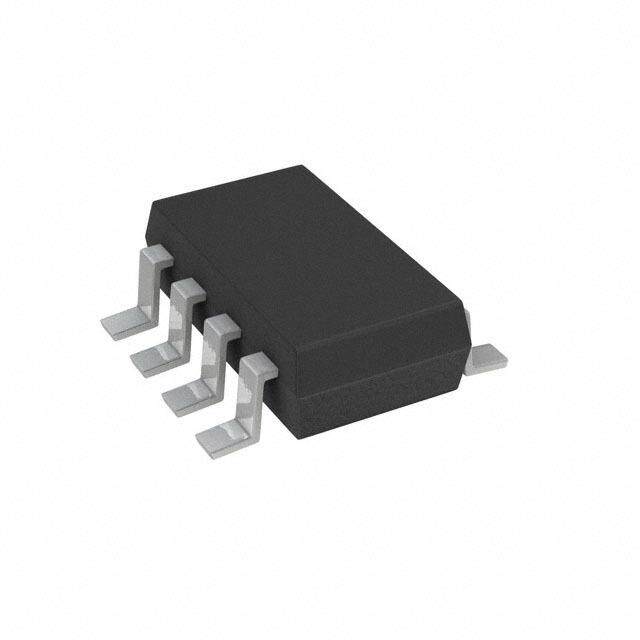
| 描述 | CONV D/A 8BIT MICROPWR 8VSSOP数模转换器- DAC 8B Micro Pwr DAC w/ RR Output |
| 产品分类 | |
| 品牌 | Texas Instruments |
| 产品手册 | |
| 产品图片 |
|
| rohs | 符合RoHS无铅 / 符合限制有害物质指令(RoHS)规范要求 |
| 产品系列 | 数据转换器IC,数模转换器- DAC,Texas Instruments DAC081S101CIMM/NOPB- |
| 数据手册 | |
| 产品型号 | DAC081S101CIMM/NOPB |
| PCN设计/规格 | |
| 产品目录页面 | |
| 产品种类 | 数模转换器- DAC |
| 位数 | 8 |
| 供应商器件封装 | 8-VSSOP |
| 其它名称 | DAC081S101CIMM/NOPBTR |
| 包装 | 带卷 (TR) |
| 商标 | Texas Instruments |
| 安装类型 | 表面贴装 |
| 封装 | Reel |
| 封装/外壳 | 8-TSSOP,8-MSOP(0.118",3.00mm 宽) |
| 封装/箱体 | VSSOP-8 |
| 工作温度 | -40°C ~ 105°C |
| 工厂包装数量 | 1000 |
| 建立时间 | 3µs |
| 数据接口 | DSP,MICROWIRE™,QSPI™,串行,SPI™ |
| 标准包装 | 1,000 |
| 电压源 | 单电源 |
| 系列 | DAC081S101 |
| 转换器数 | 1 |
| 输出数和类型 | 1 电压,单极 |
| 配用 | /product-detail/zh/DAC081S101EVAL/DAC081S101EVAL-ND/1291223 |
| 采样率(每秒) | * |


- 商务部:美国ITC正式对集成电路等产品启动337调查
- 曝三星4nm工艺存在良率问题 高通将骁龙8 Gen1或转产台积电
- 太阳诱电将投资9.5亿元在常州建新厂生产MLCC 预计2023年完工
- 英特尔发布欧洲新工厂建设计划 深化IDM 2.0 战略
- 台积电先进制程称霸业界 有大客户加持明年业绩稳了
- 达到5530亿美元!SIA预计今年全球半导体销售额将创下新高
- 英特尔拟将自动驾驶子公司Mobileye上市 估值或超500亿美元
- 三星加码芯片和SET,合并消费电子和移动部门,撤换高东真等 CEO
- 三星电子宣布重大人事变动 还合并消费电子和移动部门
- 海关总署:前11个月进口集成电路产品价值2.52万亿元 增长14.8%


PDF Datasheet 数据手册内容提取
DAC081S101 www.ti.com SNAS323C–JUNE2005–REVISEDFEBRUARY2013 DAC081S101 8-Bit Micro Power Digital-to-Analog Converter with Rail-to-Rail Output CheckforSamples:DAC081S101 FEATURES DESCRIPTION 1 • GuaranteedMonotonicity The DAC081S101 is a full-featured, general purpose 23 8-bit voltage-output digital-to-analog converter (DAC) • LowPowerOperation that can operate from a single +2.7V to 5.5V supply • Rail-to-RailVoltageOutput and consumes just 175 µA of current at 3.6 Volts. • Power-onResettoZeroVoltsOutput The on-chip output amplifier allows rail-to-rail output swing and the three wire serial interface operates at • SYNCInterruptFacility clock rates up to 30 MHz over the specified supply • WidePowerSupplyRange(+2.7Vto+5.5V) voltage range and is compatible with standard SPI™, • SmallPackages QSPI, MICROWIRE and DSP interfaces. Competitive devices are limited to 20 MHz clock rates at supply • PowerDownFeature voltagesinthe2.7Vto3.6Vrange. APPLICATIONS The supply voltage for the DAC081S101 serves as its voltage reference, providing the widest possible • Battery-PoweredInstruments output dynamic range. A power-on reset circuit • DigitalGainandOffsetAdjustment ensures that the DAC output powers up to zero volts • ProgrammableVoltage&CurrentSources and remains there until there is a valid write to the device. A power-down feature reduces power • ProgrammableAttenuators consumptiontolessthanamicroWatt. The low power consumption and small packages of the DAC081S101 make it an excellent choice for use inbatteryoperatedequipment. The DAC081S101 is a direct replacement for the AD5300 and is one of a family of pin compatible DACs, including the 10-bit DAC101S101 and the 12- bit DAC121S101. The DAC081S101 operates over the extended industrial temperature range of −40°C to+105°C. Table1.KeySpecifications VALUE Resolution 8bits DNL +0.04,-0.02LSB(typ) OutputSettlingTime 3µs(typ) ZeroCodeError 3.8mV(typ) Full-ScaleError −0.07%FS(typ) NormalMode 0.63mW(3.6V)/1.41mW(5.5V)typ PowerConsumption PwrDownMode 0.14µW(3.6V)/0.33µW(5.5V)typ 1 Pleasebeawarethatanimportantnoticeconcerningavailability,standardwarranty,anduseincriticalapplicationsof TexasInstrumentssemiconductorproductsanddisclaimerstheretoappearsattheendofthisdatasheet. SPIisatrademarkofMotorola,Inc.. 2 Allothertrademarksarethepropertyoftheirrespectiveowners. 3 PRODUCTIONDATAinformationiscurrentasofpublicationdate. Copyright©2005–2013,TexasInstrumentsIncorporated Products conform to specifications per the terms of the Texas Instruments standard warranty. Production processing does not necessarilyincludetestingofallparameters.
DAC081S101 SNAS323C–JUNE2005–REVISEDFEBRUARY2013 www.ti.com Pin Configuration SOT VSSOP VOUT 1 6 SYNC VA 1 8 GND NC 2 7 DIN GND 2 5 SCLK NC 3 6 SCLK VA 3 4 DIN VOUT 4 5 SYNC Block Diagram VA GND POWER-ON DAC081S101 RESET REF(+) REF(-) DAC REGISTER 8-BIT DAC BUFFER VOUT 8 8 INPUT POWER-DOWN CONTROL CONTROL 1k 100k LOGIC LOGIC SYNC SCLK DIN PinDescriptions SOT-23 VSSOP Name Description PinNo. PinNo. V 1 4 DACAnalogOutputVoltage. OUT GND 2 8 Groundreferenceforallon-chipcircuitry. V 3 1 PowersupplyandReferenceinput.ShouldbedecoupledtoGND. A SerialDataInput.Dataisclockedintothe16-bitshiftregisteronthefalling D 4 7 IN edgesofSCLKafterthefallofSYNC. SerialClockInput.Dataisclockedintotheinputshiftregisteronthefalling SCLK 5 6 edgesofthispin. Framesynchronizationinputforthedatainput.Whenthispingoeslow,it enablestheinputshiftregisteranddataistransferredonthefallingedges SYNC 6 5 ofSCLK.TheDACisupdatedonthe16thclockcycleunlessSYNCis broughthighbeforethe16thclock,inwhichcasetherisingedgeofSYNC actsasaninterruptandthewritesequenceisignoredbytheDAC. NC 2,3 NoConnect.Thereisnointernalconnectiontothesepins. Thesedeviceshavelimitedbuilt-inESDprotection.Theleadsshouldbeshortedtogetherorthedeviceplacedinconductivefoam duringstorageorhandlingtopreventelectrostaticdamagetotheMOSgates. 2 SubmitDocumentationFeedback Copyright©2005–2013,TexasInstrumentsIncorporated ProductFolderLinks:DAC081S101
DAC081S101 www.ti.com SNAS323C–JUNE2005–REVISEDFEBRUARY2013 Absolute Maximum Ratings (1)(2) SupplyVoltage,V 6.5V A VoltageonanyInputPin −0.3Vto(V +0.3V) A InputCurrentatAnyPin(3) 10mA PackageInputCurrent(3) 20mA PowerConsumptionatT =25°C See(4) A ESDSusceptibility(5) HumanBodyModel 2500V MachineModel 250V SolderingTemperature,Infrared, 10Seconds (6) 235°C StorageTemperature −65°Cto+150°C (1) AbsoluteMaximumRatingsindicatelimitsbeyondwhichdamagetothedevicemayoccur.OperatingRatingsindicateconditionsfor whichthedeviceisfunctional,butdonotguaranteespecificperformancelimits.Forguaranteedspecificationsandtestconditions,see theElectricalCharacteristics.Theguaranteedspecificationsapplyonlyforthetestconditionslisted.Someperformancecharacteristics maydegradewhenthedeviceisnotoperatedunderthelistedtestconditions. (2) AllvoltagesaremeasuredwithrespecttoGND=0V,unlessotherwisespecified (3) Whentheinputvoltageatanypinexceedsthepowersupplies(thatis,lessthanGND,orgreaterthanV ),thecurrentatthatpinshould A belimitedto10mA.The20mAmaximumpackageinputcurrentratinglimitsthenumberofpinsthatcansafelyexceedthepower supplieswithaninputcurrentof10mAtotwo. (4) Theabsolutemaximumjunctiontemperature(Tmax)forthisdeviceis150°C.Themaximumallowablepowerdissipationisdictatedby J Tmax,thejunction-to-ambientthermalresistance(θ ),andtheambienttemperature(T ),andcanbecalculatedusingtheformula J JA A P MAX=(Tmax−T )/θ .Thevaluesformaximumpowerdissipationwillbereachedonlywhenthedeviceisoperatedinasevere D J A JA faultcondition(e.g.,wheninputoroutputpinsaredrivenbeyondthepowersupplyvoltages,orthepowersupplypolarityisreversed). Obviously,suchconditionsshouldalwaysbeavoided. (5) Humanbodymodelis100pFcapacitordischargedthrougha1.5kΩresistor.Machinemodelis220pFdischargedthroughZERO Ohms. (6) Seethesectionentitled"SurfaceMount"foundinanypost1986NationalSemiconductorLinearDataBookformethodsofsoldering surfacemountdevices. Operating Ratings (1)(2) OperatingTemperatureRange −40°C≤T ≤+105°C A SupplyVoltage,V (3) +2.7Vto5.5V A AnyInputVoltage(4) −0.1Vto(V +0.1V) A OutputLoad 0to1500pF SCLKFrequency Upto30MHz (1) AbsoluteMaximumRatingsindicatelimitsbeyondwhichdamagetothedevicemayoccur.OperatingRatingsindicateconditionsfor whichthedeviceisfunctional,butdonotguaranteespecificperformancelimits.Forguaranteedspecificationsandtestconditions,see theElectricalCharacteristics.Theguaranteedspecificationsapplyonlyforthetestconditionslisted.Someperformancecharacteristics maydegradewhenthedeviceisnotoperatedunderthelistedtestconditions. (2) AllvoltagesaremeasuredwithrespecttoGND=0V,unlessotherwisespecified (3) Toguaranteeaccuracy,itisrequiredthatV bewellbypassed. A (4) Theanaloginputsareprotectedasshownbelow.InputvoltagemagnitudesuptoV +300mVorto300mVbelowGNDwillnot A damagethisdevice.However,errorsintheconversionresultcanoccurifanyinputgoesaboveV orbelowGNDbymorethan100mV. A Forexample,ifV is2.7V ,ensurethat−100mV≤inputvoltages≤2.8V toensureaccurateconversions. A DC DC I/O TO INTERNAL CIRCUITRY GND Package Thermal Resistances Package θ JA 8-LeadVSSOP 240°C/W 6-LeadSOT 250°C/W Copyright©2005–2013,TexasInstrumentsIncorporated SubmitDocumentationFeedback 3 ProductFolderLinks:DAC081S101
DAC081S101 SNAS323C–JUNE2005–REVISEDFEBRUARY2013 www.ti.com Electrical Characteristics Valuesshowninthistablearedesigntargetsandaresubjecttochangebeforeproductrelease. ThefollowingspecificationsapplyforV =+2.7Vto+5.5V,R =2kΩtoGND,C =200pFtoGND,f =30MHz,input A L L SCLK coderange4to251.BoldfacelimitsapplyforT ≤T ≤T :allotherlimitsT =25°C,unlessotherwisespecified. MIN A MAX A Parameter TestConditions Typical (1) Limits (1) Units (Limits) STATICPERFORMANCE Resolution 8 Bits(min) Monotonicity 8 Bits(min) INL IntegralNon-Linearity +0.16 +0.75 LSB(max) −0.12 −0.75 LSB(min) +0.04 +0.1 LSB(max) DNL DifferentialNon-Linearity −0.02 −0.1 LSB(min) ZE ZeroCodeError I =0 +3.8 +15 mV(max) OUT FSE Full-ScaleError I =0 −0.07 −1.0 %FSR(max) OUT GE GainError AllonesLoadedtoDACregister −0.10 ±1.0 %FSR(max) ZCED ZeroCodeErrorDrift −20 µV/°C V =3V −0.7 ppm/°C A TCGE GainErrorTempco V =5V −1.0 ppm/°C A OUTPUTCHARACTERISTICS OutputVoltageRange (2) 0 V(min) V V(max) A V =3V,I =10µA 2.0 mV A OUT V =3V,I =100µA 5.0 mV A OUT ZCO ZeroCodeOutput V =5V,I =10µA 3.0 mV A OUT V =5V,I =100µA 5.4 mV A OUT V =3V,I =10µA 2.986 V A OUT V =3V,I =100µA 2.976 V A OUT FSO FullScaleOutput V =5V,I =10µA 4.976 V A OUT V =5V,I =100µA 4.970 V A OUT R =∞ 1500 pF L MaximumLoadCapacitance R =2kΩ 1500 pF L DCOutputImpedance 1.3 Ohm V =5V,V =0V, A OUT −63 mA Inputcode=FFh V =3V,V =0V, A OUT −50 mA Inputcode=FFh I OutputShortCircuitCurrent OS V =5V,V =5V, A OUT 74 mA Inputcode=00h V =3V,V =3V, A OUT 53 mA Inputcode=00h (1) TypicalfiguresareatT =25°C,andrepresentmostlikelyparametricnorms.TestlimitsareguaranteedtoTI'sAOQL(Average J OutgoingQualityLevel). (2) Thisparameterisguaranteedbydesignand/orcharacterizationandisnottestedinproduction. 4 SubmitDocumentationFeedback Copyright©2005–2013,TexasInstrumentsIncorporated ProductFolderLinks:DAC081S101
DAC081S101 www.ti.com SNAS323C–JUNE2005–REVISEDFEBRUARY2013 Electrical Characteristics (continued) Valuesshowninthistablearedesigntargetsandaresubjecttochangebeforeproductrelease. ThefollowingspecificationsapplyforV =+2.7Vto+5.5V,R =2kΩtoGND,C =200pFtoGND,f =30MHz,input A L L SCLK coderange4to251.BoldfacelimitsapplyforT ≤T ≤T :allotherlimitsT =25°C,unlessotherwisespecified. MIN A MAX A Parameter TestConditions Typical (1) Limits (1) Units (Limits) LOGICINPUT I InputCurrent(3) ±1 µA(max) IN V =5V 0.8 V(max) V InputLowVoltage(3) A IL V =3V 0.5 V(max) A V =5V 2.4 V(min) V InputHighVoltage(3) A IH V =3V 2.1 V(min) A C InputCapacitance(3) 3 pF(max) IN POWERREQUIREMENTS NormalMode VA=5.5V 256 328 µA(max) fSCLK=30MHz VA=3.6V 174 224 µA(max) NormalMode VA=5.5V 221 294 µA(max) fSCLK=20MHz VA=3.6V 154 200 µA(max) NormalMode VA=5.0V 142 µA(max) fSCLK=0 VA=3.0V 107 µA(max) I SupplyCurrent(outputunloaded) A AllPDModes, VA=5.0V 83 µA(max) fSCLK=30MHz VA=3.0V 42 µA(max) AllPDModes, VA=5.0V 56 µA(max) fSCLK=20MHz VA=3.0V 28 µA(max) AllPDModes, VA=5.5V 0.06 1.0 µA(max) fSCLK=0 (3) VA=3.6V 0.04 1.0 µA(max) NormalMode VA=5.5V 1.41 1.80 mW(max) fSCLK=30MHz VA=3.6V 0.63 0.81 mW(max) NormalMode VA=5.5V 1.22 1.62 mW(max) fSCLK=20MHz VA=3.6V 0.55 0.72 mW(max) NormalMode VA=5.0V 0.71 µW(max) PowerConsumption(output fSCLK=0 VA=3.0V 0.32 µW(max) P C unloaded) AllPDModes, VA=5.0V 0.42 µW(max) fSCLK=30MHz VA=3.0V 0.13 µW(max) AllPDModes, VA=5.0V 0.28 µW(max) fSCLK=20MHz VA=3.0V 0.08 µW(max) AllPDModes, VA=5.5V 0.33 5.5 µW(max) fSCLK=0 (3) VA=3.6V 0.14 3.6 µW(max) V =5V 91 % A I /I PowerEfficiency I =2mA OUT A LOAD V =3V 94 % A (3) Thisparameterisguaranteedbydesignand/orcharacterizationandisnottestedinproduction. Copyright©2005–2013,TexasInstrumentsIncorporated SubmitDocumentationFeedback 5 ProductFolderLinks:DAC081S101
DAC081S101 SNAS323C–JUNE2005–REVISEDFEBRUARY2013 www.ti.com AC and Timing Characteristics Valuesshowninthistablearedesigntargetsandaresubjecttochangebeforeproductrelease. ThefollowingspecificationsapplyforV =+2.7Vto+5.5V,R =2kΩtoGND,C =200pFtoGND,f =30MHz,input A L L SCLK coderange4to251.BoldfacelimitsapplyforT ≤T ≤T :allotherlimitsT =25°C,unlessotherwisespecified. MIN A MAX A Units Parameter TestConditions Typical Limits (Limits) f SCLKFrequency 30 MHz(max) SCLK OutputVoltageSettlingTime 40htoC0hcode ts (1) change,R =2kΩ CL≤200pF 3 5 µs(max) L SR OutputSlewRate 1 V/µs GlitchImpulse Codechangefrom80hto7Fh 12 nV-sec DigitalFeedthrough 0.5 nV-sec V =5V 6 µs A t Wake-UpTime WU V =3V 39 µs A 1/f SCLKCycleTime 33 ns(min) SCLK t SCLKHightime 5 13 ns(min) H t SCLKLowTime 5 13 ns(min) L Set-upTimeSYNCtoSCLKRising t −15 0 ns(min) SUCL Edge t DataSet-UpTime 2.5 5 ns(min) SUD t DataHoldTime 2.5 4.5 ns(min) DHD V =5V 0 3 ns(min) A t SCLKfalltoriseofSYNC CS V =3V −2 1 ns(min) A 2.7≤V ≤3.6 9 20 ns(min) A t SYNCHighTime SYNC 3.6≤V ≤5.5 5 10 ns(min) A (1) Thisparameterisguaranteedbydesignand/orcharacterizationandisnottestedinproduction. Specification Definitions DIFFERENTIAL NON-LINEARITY (DNL) is the measure of the maximum deviation from the ideal step size of 1 LSB,whichisV /256=V /256. REF A DIGITAL FEEDTHROUGH is a measure of the energy injected into the analog output of the DAC from the digital inputswhentheDACoutputsarenotupdated.Itismeasuredwithafull-scalecodechangeonthedatabus. FULL-SCALE ERROR is the difference between the actual output voltage with a full scale code (FFh) loaded intotheDACandthevalueofV x255/256. A GAIN ERROR is the deviation from the ideal slope of the transfer function. It can be calculated from Zero and Full-ScaleErrorsasGE=FSE-ZE,whereGEisGainerror,FSEisFull-ScaleErrorandZEisZeroError. GLITCH IMPULSE is the energy injected into the analog output when the input code to the DAC register changes.Itisspecifiedastheareaoftheglitchinnanovolt-seconds. INTEGRAL NON-LINEARITY (INL) is a measure of the deviation of each individual code from a straight line through the input to output transfer function. The deviation of any given code from this straight line is measured from the center of that code value. The end point method is used. INL for this product is specified over a limited range,pertheElectricalTables. LEASTSIGNIFICANTBIT(LSB)isthebitthathasthesmallestvalueorweightofallbitsinaword.Thisvalueis LSB=V /2n (1) REF where V is the supply voltage for this product, and "n" is the DAC resolution in bits, which is 8 for the REF DAC081S101. MAXIMUM LOAD CAPACITANCE is the maximum capacitance that can be driven by the DAC with output stabilitymaintained. 6 SubmitDocumentationFeedback Copyright©2005–2013,TexasInstrumentsIncorporated ProductFolderLinks:DAC081S101
DAC081S101 www.ti.com SNAS323C–JUNE2005–REVISEDFEBRUARY2013 MONOTONICITY is the condition of being monotonic, where the DAC has an output that never decreases when theoutputcodeincreases. MOST SIGNIFICANT BIT (MSB) is the bit that has the largest value or weight of all bits in a word. Its value is 1/2ofV . A POWEREFFICIENCYistheratiooftheoutputcurrenttothetotalsupplycurrent.Theoutputcurrentcomesfrom the power supply. The difference between the supply and output currents, is the power consumed by the device withoutaload. SETTLING TIME is the time for the output to settle within 1/2 LSB of the final value after the input code is updated. WAKE-UP TIME is the time for the output to settle to within 1/2 LSB of the final value after the device is commandedtotheactivemodefromanyofthepowerdownmodes. ZERO CODE ERROR is the output error, or voltage, present at the DAC output after a code of 00h has been entered. Transfer Characteristic FSE 255 x VA 256 GE = FSE - ZE FSE = GE + ZE OUTPUT VOLTAGE ZE 0 0 255 DIGITAL INPUT CODE Figure1. Input/OutputTransferCharacteristic Timing Diagram 1 fCLK | | SCLK 1 2 13 14 15 16 tSUCL tL tSYNC tH tCS | SYNC | tDHD | DIN DB15 DB0 | | tSUD Figure2. DAC081S101Timing Copyright©2005–2013,TexasInstrumentsIncorporated SubmitDocumentationFeedback 7 ProductFolderLinks:DAC081S101
DAC081S101 SNAS323C–JUNE2005–REVISEDFEBRUARY2013 www.ti.com Typical Performance Characteristics f =30MHz,T =25C,InputCodeRange4to251,unlessotherwisestated SCLK A DNLatV =3.0V DNLatV =5.0V A A Figure3. Figure4. INLatV =3.0V INLatV =5.0V A A Figure5. Figure6. TUEatV =3.0V TUEatV =5.0V A A Figure7. Figure8. 8 SubmitDocumentationFeedback Copyright©2005–2013,TexasInstrumentsIncorporated ProductFolderLinks:DAC081S101
DAC081S101 www.ti.com SNAS323C–JUNE2005–REVISEDFEBRUARY2013 Typical Performance Characteristics (continued) f =30MHz,T =25C,InputCodeRange4to251,unlessotherwisestated SCLK A DNL INL vs. vs. V V A A Figure9. Figure10. 3VDNL 5VDNL vs. vs. f f SCLK SCLK Figure11. Figure12. 3VDNL 5VDNL vs. vs. ClockDutyCycle ClockDutyCycle Figure13. Figure14. Copyright©2005–2013,TexasInstrumentsIncorporated SubmitDocumentationFeedback 9 ProductFolderLinks:DAC081S101
DAC081S101 SNAS323C–JUNE2005–REVISEDFEBRUARY2013 www.ti.com Typical Performance Characteristics (continued) f =30MHz,T =25C,InputCodeRange4to251,unlessotherwisestated SCLK A 3VDNL 5VDNL vs. vs. Temperature Temperature Figure15. Figure16. 3VINL 5VINL vs. vs. f f SCLK SCLK Figure17. Figure18. 3VINL 5VINL vs. vs. ClockDutyCycle ClockDutyCycle Figure19. Figure20. 10 SubmitDocumentationFeedback Copyright©2005–2013,TexasInstrumentsIncorporated ProductFolderLinks:DAC081S101
DAC081S101 www.ti.com SNAS323C–JUNE2005–REVISEDFEBRUARY2013 Typical Performance Characteristics (continued) f =30MHz,T =25C,InputCodeRange4to251,unlessotherwisestated SCLK A 3VINL 5VINL vs. vs. Temperature Temperature Figure21. Figure22. ZeroCodeError ZeroCodeError vs. vs. f ClockDutyCycle SCLK Figure23. Figure24. ZeroCodeError Full-ScaleError vs. vs. Temperature f SCLK Figure25. Figure26. Copyright©2005–2013,TexasInstrumentsIncorporated SubmitDocumentationFeedback 11 ProductFolderLinks:DAC081S101
DAC081S101 SNAS323C–JUNE2005–REVISEDFEBRUARY2013 www.ti.com Typical Performance Characteristics (continued) f =30MHz,T =25C,InputCodeRange4to251,unlessotherwisestated SCLK A Full-ScaleError Full-ScaleError vs. vs. ClockDutyCycle Temperature Figure27. Figure28. SupplyCurrent SupplyCurrent vs. vs. V Temperature A Figure29. Figure30. 5VGlitchResponse Power-OnReset Figure31. Figure32. 12 SubmitDocumentationFeedback Copyright©2005–2013,TexasInstrumentsIncorporated ProductFolderLinks:DAC081S101
DAC081S101 www.ti.com SNAS323C–JUNE2005–REVISEDFEBRUARY2013 Typical Performance Characteristics (continued) f =30MHz,T =25C,InputCodeRange4to251,unlessotherwisestated SCLK A 3VWake-UpTime 5VWake-UpTime Figure33. Figure34. Copyright©2005–2013,TexasInstrumentsIncorporated SubmitDocumentationFeedback 13 ProductFolderLinks:DAC081S101
DAC081S101 SNAS323C–JUNE2005–REVISEDFEBRUARY2013 www.ti.com FUNCTIONAL DESCRIPTION DAC SECTION The DAC081S101 is fabricated on a CMOS process with an architecture that consists of switches and a resistor string that are followed by an output buffer. The power supply serves as the reference voltage. The input coding isstraightbinarywithanidealoutputvoltageof: V =V x(D/256) (2) OUT A where D is the decimal equivalent of the binary code that is loaded into the DAC register and can take on any valuebetween0and255. RESISTOR STRING TheresistorstringisshowninFigure35.Thisstringconsistsof4096equalvaluedresistorswithaswitchateach junctionoftworesistors,plusaswitchtoground.ThecodeloadedintotheDACregisterdetermineswhichswitch isclosed,connectingthepropernodetotheamplifier.ThisconfigurationguaranteesthattheDACismonotonic. VA R R R To Output Amplifier R R Figure35. DACResistorString OUTPUT AMPLIFIER The output buffer amplifier is a rail-to-rail type, providing an output voltage range of 0V to V . All amplifiers, even A rail-to-rail types, exhibit a loss of linearity as the output approaches the supply rails (0V and V , in this case). For A this reason, linearity is specified over less than the full output range of the DAC. The output capabilities of the amplifieraredescribedintheElectricalTables. SERIAL INTERFACE The three-wire interface is compatible with SPI, QSPI and MICROWIRE as well as most DSPs. See the Timing Diagramforinformationonawritesequence. A write sequence begins by bringing the SYNC line low. Once SYNC is low, the data on the D line is clocked IN intothe16-bitserialinputregisteronthefallingedgesofSCLK.Onthe16thfallingclockedge,thelastdatabitis clockedinandtheprogrammedfunction(achangeinthemodeofoperationand/orachangeintheDACregister contents) is executed. At this point the SYNC line may be kept low or brought high. In either case, it must be brought high for the minimum specified time before the next write sequence as a falling edge of SYNC is used to initiatethenextwritecycle. 14 SubmitDocumentationFeedback Copyright©2005–2013,TexasInstrumentsIncorporated ProductFolderLinks:DAC081S101
DAC081S101 www.ti.com SNAS323C–JUNE2005–REVISEDFEBRUARY2013 Since the SYNC and D buffers draw more current when they are high, they should be idled low between write IN sequencestominimizepowerconsumption. INPUT SHIFT REGISTER The input shift register, Figure 36, has sixteen bits. The first two bits are "don't cares" and are followed by two bitsthatdeterminethemodeofoperation(normalmodeoroneofthreepower-downmodes).Thecontentsofthe serial input register are transferred to the DAC register on the sixteenth falling edge of SCLK. See Timing Diagram,Figure2. MSB LSB X X PD1PD0 D7 D6 D5 D4 D3 D2 D1 D0 X X X X DATABITS 0 0 Normal Operation 0 1 1 kWto GND 1 0 100 kWto GND Power-Down Modes 1 1 High Impedance Figure36. InputRegisterContents Normally, the SYNC line is kept low for at least 16 falling edges of SCLK and the DAC is updated on the 16th SCLK falling edge. However, if SYNC is brought high before the 16th falling edge, the shift register is reset and the write sequence is invalid. The DAC register is not updated and there is no change in the mode of operation orintheoutputvoltage. POWER-ON RESET The power-on reset circuit controls the output voltage during power-up. Upon application of power the DAC register is filled with zeros and the output voltage is 0 Volts and remains there until a valid write sequence is madetotheDAC. POWER-DOWN MODES The DAC081S101 has four modes of operation. These modes are set with two bits (DB13 and DB12) in the controlregister. Table2.ModesofOperation DB13 DB12 OperatingMode 0 0 NormalOperation 0 1 Power-Downwith1kΩtoGND 1 0 Power-Downwith100kΩtoGND 1 1 Power-DownwithHi-Z When both DB13 and DB12 are 0, the device operates normally. For the other three possible combinations of these bits the supply current drops to its power-down level and the output is pulled down with either a 1kΩ or a 100KΩ resistor,orisinahighimpedancestate,asdescribedinTable2. The bias generator, output amplifier, the resistor string and other linear circuitry are all shut down in any of the power-down modes. However, the contents of the DAC register are unaffected when in power-down, so when coming out of power down the output voltage returns to the same voltage it was before entering power down. Minimum power consumption is achieved in the power-down mode with SCLK disabled and SYNC and D idled IN low. The time to exit power-down (Wake-Up Time) is typically t µsec as stated in the A.C. and Timing WU CharacteristicsTable. APPLICATION INFORMATION The simplicity of the DAC081S101 implies ease of use. However, it is important to recognize that any data converter that utilizes its supply voltage as its reference voltage will have essentially zero PSRR (Power Supply RejectionRatio).Therefore,itisnecessarytoprovideanoise-freesupplyvoltagetothedevice. Copyright©2005–2013,TexasInstrumentsIncorporated SubmitDocumentationFeedback 15 ProductFolderLinks:DAC081S101
DAC081S101 SNAS323C–JUNE2005–REVISEDFEBRUARY2013 www.ti.com DSP/MICROPROCESSORINTERFACING Interfacing the DAC081S101 to microprocessors and DSPs is quite simple. The following guidelines are offered tohastenthedesignprocess. ADSP-2101/ADSP2103Interfacing Figure 37 shows a serial interface between the DAC081S101 and the ADSP-2101/ADSP2103. The DSP should be set to operate in the SPORT Transmit Alternate Framing Mode. It is programmed through the SPORT control register and should be configured for Internal Clock Operation, Active Low Framing and 16-bit Word Length. TransmissionisstartedbywritingawordtotheTxregisteraftertheSPORTmodehasbeenenabled. ADSP-2101/ DAC081S101 ADSP2103 TFS SYNC DT DIN SCLK SCLK Figure37. ADSP-2101/2103Interface 80C51/80L51Interface A serial interface between the DAC081S101 and the 80C51/80L51 microcontroller is shown in Figure 38. The SYNC signal comes from a bit-programmable pin on the microcontroller. The example shown here uses port line P3.3. This line is taken low when data is to transmitted to the DAC081S101. Since the 80C51/80L51 transmits 8- bit bytes, only eight falling clock edges occur in the transmit cycle. To load data into the DAC, the P3.3 line must be left low after the first eight bits are transmitted. A second write cycle is initiated to transmit the second byte of data, after which port line P3.3 is brought high. The 80C51/80L51 transmit routine must recognize that the 80C51/80L51transmitsdatawiththeLSBfirstwhiletheDAC081S101requiresdatawiththeMSBfirst. 80C51/80L51 DAC081S101 P3.3 SYNC TXD SCLK RXD DIN Figure38. 80C51/80L51Interface 68HC11Interface A serial interface between the DAC081S101 and the 68HC11 microcontroller is shown in Figure 39. The SYNC lineoftheDAC081S101isdrivenfromaportline(PC7inthefigure),similartothe80C51/80L51. The 68HC11 should be configured with its CPOL bit as a zero and its CPHA bit as a one. This configuration causes data on the MOSI output to be valid on the falling edge of SCLK. PC7 is taken low to transmit data to the DAC. The 68HC11 transmits data in 8-bit bytes with eight falling clock edges. Data is transmitted with the MSB first. PC7 must remain low after the first eight bits are transferred. A second write cycle is initiated to transmit the secondbyteofdatatotheDAC,afterwhichPC7shouldberaisedtoendthewritesequence. 68HC11 DAC081S101 PC7 SYNC SCK SCLK MOSI DIN Figure39. 68HC11Interface MicrowireInterface Figure 40 shows an interface between a Microwire compatible device and the DAC081S101. Data is clocked out ontherisingedgesoftheSCLKsignal. 16 SubmitDocumentationFeedback Copyright©2005–2013,TexasInstrumentsIncorporated ProductFolderLinks:DAC081S101
DAC081S101 www.ti.com SNAS323C–JUNE2005–REVISEDFEBRUARY2013 MICROWIRE DAC081S101 DEVICE CS SYNC SK SCLK SO DIN Figure40. MicrowireInterface USINGREFERENCESASPOWERSUPPLIES Recalltheneedforaquietsupplysourcefordevicesthatusetheirpowersupplyvoltageasareferencevoltage. Since the DAC081S101 consumes very little power, a reference source may be used as the supply voltage. The advantages of using a reference source over a voltage regulator are accuracy and stability. Some low noise regulators can also be used for the power supply of the DAC081S101. Listed below are a few power supply optionsfortheDAC081S101. LM4130 The LM4130 reference, with its 0.05% accuracy over temperature, is a good choice as a power source for the DAC081S101. Its primary disadvantage is the lack of 3V and 5V versions. However, the 4.096V version is useful if a 0 to 4.095V output range is desirable or acceptable. Bypassing the LM4130 VIN pin with a 0.1µF capacitor and the VOUT pin with a 2.2µF capacitor will improve stability and reduce output noise. The LM4130 comes in a space-saving5-pinSOT23. Input LM4130-4.1 Voltage C1 C2 0.1 PF 2.2 PF DAC081S101 SYNC VOUT = 0V to 4.080V DIN SCLK Figure41. TheLM4130asapowersupply LM4050 Availablewithaccuracyof0.44%,theLM4050shuntreferenceisalsoagoodchoiceasapowerregulatorforthe DAC081S101. It does not come in a 3 Volt version, but 4.096V and 5V versions are available. It comes in a space-saving3-pinSOT-23. Input Voltage R VZ LM4050-4.1 0.47 PF or LM4050-5.0 DAC081S101 SYNC VOUT = 0V to 5V DIN SCLK Figure42. TheLM4050asapowersupply Copyright©2005–2013,TexasInstrumentsIncorporated SubmitDocumentationFeedback 17 ProductFolderLinks:DAC081S101
DAC081S101 SNAS323C–JUNE2005–REVISEDFEBRUARY2013 www.ti.com The minimum resistor value in the circuit of Figure 42 should be chosen such that the maximum current through the LM4050 does not exceed its 15 mA rating. The conditions for maximum current include the input voltage at its maximum, the LM4050 voltage at its minimum, the resistor value at its minimum due to tolerance, and the DAC081S101 draws zero current. The maximum resistor value must allow the LM4050 to draw more than its minimum current for regulation plus the maximum DAC081S101 current in full operation. The conditions for minimum current include the input voltage at its minimum, the LM4050 voltage at its maximum, the resistor value at its maximum due to tolerance, and the DAC081S101 draws its maximum current. These conditions can be summarizedas R(min)=(V (max)−V (min)/(I (min)+I (max)) (3) IN Z A Z and R(max)=(V (min)−V (max)/(I (max)+I (min)) (4) IN Z A Z where V (min) and V (max) are the nominal LM4050 output voltages ± the LM4050 output tolerance over Z Z temperature, I (max) is the maximum allowable current through the LM4050, I (min) is the minimum current Z Z required by the LM4050 for proper regulation, I (max) is the maximum DAC081S101 supply current, and I (min) A A istheminimumDAC081S101supplycurrent. LP3985 The LP3985 is a low noise, ultra low dropout voltage regulator with a 3% accuracy over temperature. It is a good choice for applications that do not require a precision reference for the DAC081S101. It comes in 3.0V, 3.3V and 5V versions, among others, and sports a low 30 µV noise specification at low frequencies. Since low frequency noise is relatively difficult to filter, this specification could be important for some applications. The LP3985 comes inaspace-saving5-pinSOT-23and5-bumpDSBGApackages. Input LP3985 Voltage 1 PF 0.1 PF 0.01 PF DAC081S101 SYNC VOUT = 0V to 5V DIN SCLK Figure43. UsingtheLP3985regulator An input capacitance of 1.0µF without any ESR requirement is required at the LP3985 input, while a 1.0µF ceramic capacitor with an ESR requirement of 5mΩ to 500mΩ is required at the output. Careful interpretation andunderstandingofthecapacitorspecificationisrequiredtoensurecorrectdeviceoperation. LP2980 The LP2980 is an ultra low dropout regulator with a 0.5% or 1.0% accuracy over temperature, depending upon grade.Itisavailablein3.0V,3.3Vand5Vversions,amongothers. Input VIN VOUT Voltage LP2980 ON /OFF 1 PF DAC081S101 SYNC VOUT = 0V to 5V DIN SCLK Figure44. UsingtheLP2980regulator 18 SubmitDocumentationFeedback Copyright©2005–2013,TexasInstrumentsIncorporated ProductFolderLinks:DAC081S101
DAC081S101 www.ti.com SNAS323C–JUNE2005–REVISEDFEBRUARY2013 Like any low dropout regulator, the LP2980 requires an output capacitor for loop stability. This output capacitor must be at least 1.0µF over temperature, but values of 2.2µF or more will provide even better performance. The ESR of this capacitor should be within the range specified in the LP2980 data sheet. Surface-mount solid tantalum capacitors offer a good combination of small size and ESR. Ceramic capacitors are attractive due to their small size but generally have ESR values that are too low for use with the LP2980. Aluminum electrolytic capacitors are typically not a good choice due to their large size and have ESR values that may be too high at lowtemperatures. BIPOLAROPERATION The DAC081S101 is designed for single supply operation and thus has a unipolar output. However, a bipolar output may be obtained with the circuit in Figure 45. This circuit will provide an output voltage range of ±5 Volts. Arail-to-railamplifiershouldbeusediftheamplifiersuppliesarelimitedto±5V. 10 pF R2 +5V +5V R1 10 PF + 0.1 PF - ±5V + DAC081S101 -5V SYNC VOUT DIN SCLK Figure45. BipolarOperation Theoutputvoltageofthiscircuitforanycodeisfoundtobe V =(V x(D/256)x((R1+R2)/R1)-V xR2/R1) (5) O A A whereDistheinputcodeindecimalform.WithV =5VandR1=R2, A V =(10xD/256)-5V (6) O Alistofrail-to-railamplifierssuitableforthisapplicationareindicatedinTable3. Table3.SomeRail-to-RailAmplifiers AMP PKGS TypV TypI OS SUPPLY PDIP-8 LMC7111 0.9mV 25µA SOT-23-5 SO-8 LM7301 0.03mV 620µA SOT-23-5 LM8261 SOT-23-5 0.7mV 1mA LAYOUT,GROUNDING,ANDBYPASSING For best accuracy and minimum noise, the printed circuit board containing the DAC081S101 should have separate analog and digital areas. The areas are defined by the locations of the analog and digital power planes. Both of these planes should be located in the same board layer. There should be a single ground plane. A single ground plane is preferred if digital return current does not flow through the analog ground area. Frequently a single ground plane design will utilize a "fencing" technique to prevent the mixing of analog and digital ground current. Separate ground planes should only be utilized when the fencing technique is inadequate. The separate ground planes must be connected in one place, preferably near the DAC081S101. Special care is required to guaranteethatdigitalsignalswithfastedgeratesdonotpassoversplitgroundplanes.Theymustalwayshavea continuousreturnpathbelowtheirtraces. The DAC081S101 power supply should be bypassed with a 10µF and a 0.1µF capacitor as close as possible to the device with the 0.1µF right at the device supply pin. The 10µF capacitor should be a tantalum type and the 0.1µF capacitor should be a low ESL, low ESR type. The power supply for the DAC081S101 should only be usedforanalogcircuits. Avoid crossover of analog and digital signals and keep the clock and data lines on the component side of the board.Theclockanddatalinesshouldhavecontrolledimpedances. Copyright©2005–2013,TexasInstrumentsIncorporated SubmitDocumentationFeedback 19 ProductFolderLinks:DAC081S101
DAC081S101 SNAS323C–JUNE2005–REVISEDFEBRUARY2013 www.ti.com REVISION HISTORY ChangesfromRevisionB(February2013)toRevisionC Page • ChangedlayoutofNationalDataSheettoTIformat.......................................................................................................... 19 20 SubmitDocumentationFeedback Copyright©2005–2013,TexasInstrumentsIncorporated ProductFolderLinks:DAC081S101
PACKAGE OPTION ADDENDUM www.ti.com 6-Feb-2020 PACKAGING INFORMATION Orderable Device Status Package Type Package Pins Package Eco Plan Lead/Ball Finish MSL Peak Temp Op Temp (°C) Device Marking Samples (1) Drawing Qty (2) (6) (3) (4/5) DAC081S101CIMK/NOPB ACTIVE SOT-23-THIN DDC 6 1000 Green (RoHS SN Level-1-260C-UNLIM -40 to 105 X65C & no Sb/Br) DAC081S101CIMKX/NOPB ACTIVE SOT-23-THIN DDC 6 3000 Green (RoHS SN Level-1-260C-UNLIM -40 to 105 X65C & no Sb/Br) DAC081S101CIMM/NOPB ACTIVE VSSOP DGK 8 1000 Green (RoHS SN Level-1-260C-UNLIM -40 to 105 X64C & no Sb/Br) DAC081S101CIMMX/NOPB ACTIVE VSSOP DGK 8 3500 Green (RoHS SN Level-1-260C-UNLIM -40 to 105 X64C & no Sb/Br) (1) The marketing status values are defined as follows: ACTIVE: Product device recommended for new designs. LIFEBUY: TI has announced that the device will be discontinued, and a lifetime-buy period is in effect. NRND: Not recommended for new designs. Device is in production to support existing customers, but TI does not recommend using this part in a new design. PREVIEW: Device has been announced but is not in production. Samples may or may not be available. OBSOLETE: TI has discontinued the production of the device. (2) RoHS: TI defines "RoHS" to mean semiconductor products that are compliant with the current EU RoHS requirements for all 10 RoHS substances, including the requirement that RoHS substance do not exceed 0.1% by weight in homogeneous materials. Where designed to be soldered at high temperatures, "RoHS" products are suitable for use in specified lead-free processes. TI may reference these types of products as "Pb-Free". RoHS Exempt: TI defines "RoHS Exempt" to mean products that contain lead but are compliant with EU RoHS pursuant to a specific EU RoHS exemption. Green: TI defines "Green" to mean the content of Chlorine (Cl) and Bromine (Br) based flame retardants meet JS709B low halogen requirements of <=1000ppm threshold. Antimony trioxide based flame retardants must also meet the <=1000ppm threshold requirement. (3) MSL, Peak Temp. - The Moisture Sensitivity Level rating according to the JEDEC industry standard classifications, and peak solder temperature. (4) There may be additional marking, which relates to the logo, the lot trace code information, or the environmental category on the device. (5) Multiple Device Markings will be inside parentheses. Only one Device Marking contained in parentheses and separated by a "~" will appear on a device. If a line is indented then it is a continuation of the previous line and the two combined represent the entire Device Marking for that device. (6) Lead/Ball Finish - Orderable Devices may have multiple material finish options. Finish options are separated by a vertical ruled line. Lead/Ball Finish values may wrap to two lines if the finish value exceeds the maximum column width. Important Information and Disclaimer:The information provided on this page represents TI's knowledge and belief as of the date that it is provided. TI bases its knowledge and belief on information provided by third parties, and makes no representation or warranty as to the accuracy of such information. Efforts are underway to better integrate information from third parties. TI has taken and Addendum-Page 1
PACKAGE OPTION ADDENDUM www.ti.com 6-Feb-2020 continues to take reasonable steps to provide representative and accurate information but may not have conducted destructive testing or chemical analysis on incoming materials and chemicals. TI and TI suppliers consider certain information to be proprietary, and thus CAS numbers and other limited information may not be available for release. In no event shall TI's liability arising out of such information exceed the total purchase price of the TI part(s) at issue in this document sold by TI to Customer on an annual basis. Addendum-Page 2
PACKAGE MATERIALS INFORMATION www.ti.com 24-Aug-2017 TAPE AND REEL INFORMATION *Alldimensionsarenominal Device Package Package Pins SPQ Reel Reel A0 B0 K0 P1 W Pin1 Type Drawing Diameter Width (mm) (mm) (mm) (mm) (mm) Quadrant (mm) W1(mm) DAC081S101CIMK/NOPB SOT- DDC 6 1000 178.0 8.4 3.2 3.2 1.4 4.0 8.0 Q3 23-THIN DAC081S101CIMKX/NOP SOT- DDC 6 3000 178.0 8.4 3.2 3.2 1.4 4.0 8.0 Q3 B 23-THIN DAC081S101CIMM/NOPB VSSOP DGK 8 1000 178.0 12.4 5.3 3.4 1.4 8.0 12.0 Q1 DAC081S101CIMMX/NOP VSSOP DGK 8 3500 330.0 12.4 5.3 3.4 1.4 8.0 12.0 Q1 B PackMaterials-Page1
PACKAGE MATERIALS INFORMATION www.ti.com 24-Aug-2017 *Alldimensionsarenominal Device PackageType PackageDrawing Pins SPQ Length(mm) Width(mm) Height(mm) DAC081S101CIMK/NOPB SOT-23-THIN DDC 6 1000 210.0 185.0 35.0 DAC081S101CIMKX/NOP SOT-23-THIN DDC 6 3000 210.0 185.0 35.0 B DAC081S101CIMM/NOPB VSSOP DGK 8 1000 210.0 185.0 35.0 DAC081S101CIMMX/NOP VSSOP DGK 8 3500 367.0 367.0 35.0 B PackMaterials-Page2
None
None
PACKAGE OUTLINE DDC0006A SOT - 1.1 max height SCALE 4.000 SOT 3.05 2.55 1.1 MAX 11..7455 B A 0.1 C PIN 1 INDEX AREA 1 6 4X 0.95 3.05 1.9 2.75 4 3 6X 00..53 00..10 TYP 0.2 C A B 0 -8 TYP C 0.25 0.20 SEATING PLANE 0.12 TYP GAGE PLANE 0.6 TYP 0.3 4214841/A 08/2016 NOTES: 1. All linear dimensions are in millimeters. Any dimensions in parenthesis are for reference only. Dimensioning and tolerancing per ASME Y14.5M. 2. This drawing is subject to change without notice. 3. Reference JEDEC MO-193. www.ti.com
EXAMPLE BOARD LAYOUT DDC0006A SOT - 1.1 max height SOT SYMM 6X (1.1) 1 6X (0.6) 6 SYMM 4X (0.95) 4 3 (R0.05) TYP (2.7) LAND PATTERN EXAMPLE EXPLOSED METAL SHOWN SCALE:15X METAL UNDER SOLDER MASK SOLDER MASK METAL SOLDER MASK OPENING OPENING EXPOSED METAL EXPOSED METAL 0.07 MAX 0.07 MIN ARROUND ARROUND NON SOLDER MASK SOLDER MASK DEFINED DEFINED SOLDERMASK DETAILS 4214841/A 08/2016 NOTES: (continued) 4. Publication IPC-7351 may have alternate designs. 5. Solder mask tolerances between and around signal pads can vary based on board fabrication site. www.ti.com
EXAMPLE STENCIL DESIGN DDC0006A SOT - 1.1 max height SOT SYMM 6X (1.1) 1 6X (0.6) 6 SYMM 4X(0.95) 4 3 (R0.05) TYP (2.7) SOLDER PASTE EXAMPLE BASED ON 0.125 THICK STENCIL SCALE:15X 4214841/A 08/2016 NOTES: (continued) 6. Laser cutting apertures with trapezoidal walls and rounded corners may offer better paste release. IPC-7525 may have alternate design recommendations. 7. Board assembly site may have different recommendations for stencil design. www.ti.com
IMPORTANTNOTICEANDDISCLAIMER TI PROVIDES TECHNICAL AND RELIABILITY DATA (INCLUDING DATASHEETS), DESIGN RESOURCES (INCLUDING REFERENCE DESIGNS), APPLICATION OR OTHER DESIGN ADVICE, WEB TOOLS, SAFETY INFORMATION, AND OTHER RESOURCES “AS IS” AND WITH ALL FAULTS, AND DISCLAIMS ALL WARRANTIES, EXPRESS AND IMPLIED, INCLUDING WITHOUT LIMITATION ANY IMPLIED WARRANTIES OF MERCHANTABILITY, FITNESS FOR A PARTICULAR PURPOSE OR NON-INFRINGEMENT OF THIRD PARTY INTELLECTUAL PROPERTY RIGHTS. These resources are intended for skilled developers designing with TI products. You are solely responsible for (1) selecting the appropriate TI products for your application, (2) designing, validating and testing your application, and (3) ensuring your application meets applicable standards, and any other safety, security, or other requirements. These resources are subject to change without notice. TI grants you permission to use these resources only for development of an application that uses the TI products described in the resource. Other reproduction and display of these resources is prohibited. No license is granted to any other TI intellectual property right or to any third party intellectual property right. TI disclaims responsibility for, and you will fully indemnify TI and its representatives against, any claims, damages, costs, losses, and liabilities arising out of your use of these resources. TI’s products are provided subject to TI’s Terms of Sale (www.ti.com/legal/termsofsale.html) or other applicable terms available either on ti.com or provided in conjunction with such TI products. TI’s provision of these resources does not expand or otherwise alter TI’s applicable warranties or warranty disclaimers for TI products. Mailing Address: Texas Instruments, Post Office Box 655303, Dallas, Texas 75265 Copyright © 2020, Texas Instruments Incorporated