ICGOO在线商城 > 集成电路(IC) > 数据采集 - 数模转换器 > AD5301BRTZ-500RL7
 Datasheet下载
- 型号: AD5301BRTZ-500RL7
- 制造商: Analog
- 库位|库存: xxxx|xxxx
- 要求:
| 数量阶梯 | 香港交货 | 国内含税 |
| +xxxx | $xxxx | ¥xxxx |
查看当月历史价格
查看今年历史价格
AD5301BRTZ-500RL7产品简介:
ICGOO电子元器件商城为您提供AD5301BRTZ-500RL7由Analog设计生产,在icgoo商城现货销售,并且可以通过原厂、代理商等渠道进行代购。 AD5301BRTZ-500RL7价格参考¥22.90-¥43.03。AnalogAD5301BRTZ-500RL7封装/规格:数据采集 - 数模转换器, 8 位 数模转换器 1 SOT-23-6。您可以下载AD5301BRTZ-500RL7参考资料、Datasheet数据手册功能说明书,资料中有AD5301BRTZ-500RL7 详细功能的应用电路图电压和使用方法及教程。
AD5301BRTZ-500RL7 是由 Analog Devices Inc. 生产的一款 8 位电压输出数模转换器(DAC),具有低功耗、小封装和高精度等特点。该器件广泛应用于各种需要精确控制模拟信号的场景,特别是在工业自动化、测试测量设备以及医疗仪器等领域。

 工业自动化
在工业自动化中,AD5301BRTZ-500RL7 可用于控制系统中的模拟信号输出,例如调节电机速度、控制阀门开度或调整传感器的灵敏度。其高分辨率和低功耗特性使得它能够在长时间运行的工业环境中保持稳定性能,同时减少能耗。

 测试与测量设备
对于测试测量设备而言,AD5301BRTZ-500RL7 可以提供精确的电压输出,用于校准和测试其他电子设备。例如,在自动测试设备(ATE)中,它可以帮助生成标准电压信号,以验证被测设备的性能。此外,它还可以用于数据采集系统中,将数字信号转换为模拟信号,以便进行进一步的分析和处理。

 医疗仪器
在医疗仪器领域,AD5301BRTZ-500RL7 的高精度和稳定性使其成为理想选择。它可以用于生成精确的模拟信号,以驱动超声波探头、心电图机或其他诊断设备中的关键组件。此外,它还可以用于控制药物输液泵的速度或调节患者监护仪中的参数显示。

 消费电子
在消费电子产品中,AD5301BRTZ-500RL7 可用于音频设备、智能家居控制器等需要模拟信号输出的应用。例如,在音频设备中,它可以将数字音频信号转换为模拟信号,以驱动扬声器或耳机;在智能家居控制器中,它可以用于调节灯光亮度或温度设定。

总之,AD5301BRTZ-500RL7 凭借其高性能和灵活性,适用于多种应用场景,尤其在需要高精度和低功耗的场合表现突出。
| 参数 | 数值 |
| 产品目录 | 集成电路 (IC)半导体 |
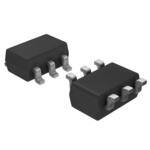
| 描述 | IC DAC 8BIT 2WIRE I2C SOT23-6数模转换器- DAC I2C 8-BIT Vout |
| 产品分类 | |
| 品牌 | Analog Devices Inc |
| 产品手册 | |
| 产品图片 |
|
| rohs | 符合RoHS无铅 / 符合限制有害物质指令(RoHS)规范要求 |
| 产品系列 | 数据转换器IC,数模转换器- DAC,Analog Devices AD5301BRTZ-500RL7- |
| 数据手册 | |
| 产品型号 | AD5301BRTZ-500RL7 |
| 产品培训模块 | http://www.digikey.cn/PTM/IndividualPTM.page?site=cn&lang=zhs&ptm=19145http://www.digikey.cn/PTM/IndividualPTM.page?site=cn&lang=zhs&ptm=18614http://www.digikey.cn/PTM/IndividualPTM.page?site=cn&lang=zhs&ptm=26125http://www.digikey.cn/PTM/IndividualPTM.page?site=cn&lang=zhs&ptm=26140http://www.digikey.cn/PTM/IndividualPTM.page?site=cn&lang=zhs&ptm=26150http://www.digikey.cn/PTM/IndividualPTM.page?site=cn&lang=zhs&ptm=26147 |
| 产品目录页面 | |
| 产品种类 | 数模转换器- DAC |
| 位数 | 8 |
| 供应商器件封装 | SOT-23-6 |
| 其它名称 | AD5301BRTZ500RL7 |
| 分辨率 | 8 bit |
| 包装 | 带卷 (TR) |
| 商标 | Analog Devices |
| 安装类型 | 表面贴装 |
| 安装风格 | SMD/SMT |
| 封装 | Reel |
| 封装/外壳 | SOT-23-6 |
| 封装/箱体 | SOT-23-6 |
| 工作温度 | -40°C ~ 105°C |
| 工厂包装数量 | 500 |
| 建立时间 | 6µs |
| 接口类型 | Serial |
| 数据接口 | I²C |
| 最大功率耗散 | 750 uW |
| 最大工作温度 | + 105 C |
| 最小工作温度 | - 40 C |
| 标准包装 | 500 |
| 电压参考 | External |
| 电压源 | 单电源 |
| 电源电压-最大 | 5.5 V |
| 电源电压-最小 | 2.5 V |
| 积分非线性 | +/- 1 LSB |
| 稳定时间 | 6 us |
| 系列 | AD5301 |
| 结构 | Resistor String |
| 转换器数 | 1 |
| 转换器数量 | 1 |
| 输出数和类型 | 1 电压,单极1 电压,双极 |
| 输出类型 | Voltage |
| 采样比 | 167 kSPs |
| 采样率(每秒) | - |


- 商务部:美国ITC正式对集成电路等产品启动337调查
- 曝三星4nm工艺存在良率问题 高通将骁龙8 Gen1或转产台积电
- 太阳诱电将投资9.5亿元在常州建新厂生产MLCC 预计2023年完工
- 英特尔发布欧洲新工厂建设计划 深化IDM 2.0 战略
- 台积电先进制程称霸业界 有大客户加持明年业绩稳了
- 达到5530亿美元!SIA预计今年全球半导体销售额将创下新高
- 英特尔拟将自动驾驶子公司Mobileye上市 估值或超500亿美元
- 三星加码芯片和SET,合并消费电子和移动部门,撤换高东真等 CEO
- 三星电子宣布重大人事变动 还合并消费电子和移动部门
- 海关总署:前11个月进口集成电路产品价值2.52万亿元 增长14.8%


PDF Datasheet 数据手册内容提取
2.5 V to 5.5 V, 120 μA, 2-Wire Interface, Voltage-Output 8-/10-/12-Bit DACs Data Sheet AD5301/AD5311/AD5321 FEATURES GENERAL DESCRIPTION AD5301: buffered voltage output 8-bit DAC The AD5301/AD5311/AD53211 are single 8-/10-/12-bit, buff- AD5311: buffered voltage output 10-bit DAC ered, voltage-output DACs that operate from a single 2.5 V to AD5321: buffered voltage output 12-bit DAC 5.5 V supply, consuming 120 μA at 3 V. The on-chip output 6-lead SOT-23 and 8-lead MSOP packages amplifier allows rail-to-rail output swing with a slew rate of Micropower operation: 120 μA at 3 V 0.7 V/μs. It uses a 2-wire (I2C-compatible) serial interface that 2-wire (I2C-compatible) serial interface operates at clock rates up to 400 kHz. Multiple devices can share Data readback capability the same bus. 2.5 V to 5.5 V power supply The reference for the DAC is derived from the power supply Guaranteed monotonic by design over all codes inputs and thus gives the widest dynamic output range. These Power-down to 50 nA at 3 V devices incorporate a power-on reset circuit, which ensures that Reference derived from power supply the DAC output powers up to 0 V and remains there until a Power-on reset to 0 V valid write takes place. The devices contain a power-down On-chip rail-to-rail output buffer amplifier feature that reduces the current consumption of the device to 3 power-down functions 50 nA at 3 V and provides software-selectable output loads APPLICATIONS while in power-down mode. Portable battery-powered instruments The low power consumption in normal operation makes these Digital gain and offset adjustment DACs ideally suited to portable battery-operated equipment. The Programmable voltage and current sources power consumption is 0.75 mW at 5 V and 0.36 mW at 3 V, Programmable attenuators reducing to 1 μW in all power-down modes. FUNCTIONAL BLOCK DIAGRAM VDD AD5301/AD5311/AD5321 SCL REF SDA INTLEORGFIACCE REGDIASCTER 8-/10D-/A1C2-BIT BUFFER VOUT A0 A1* POWER-DOWN LOGIC RESISTOR POWER-ON NETWORK RESET *AVAILABLE ONG 8N-LDEAD VERSION ONLY PD* 00927-001 Figure 1. 1 Protected by U.S. Patent No. 5684481. Rev. C Document Feedback Information furnished by Analog Devices is believed to be accurate and reliable. However, no responsibility is assumed by Analog Devices for its use, nor for any infringements of patents or other One Technology Way, P.O. Box 9106, Norwood, MA 02062-9106, U.S.A. rights of third parties that may result from its use. Specifications subject to change without notice. No license is granted by implication or otherwise under any patent or patent rights of Analog Devices. Tel: 781.329.4700 ©1999–2016 Analog Devices, Inc. All rights reserved. Trademarks and registered trademarks are the property of their respective owners. Technical Support www.analog.com
AD5301/AD5311/AD5321 Data Sheet TABLE OF CONTENTS Features .............................................................................................. 1 Output Amplifier ........................................................................ 13 Applications ....................................................................................... 1 Power-On Reset .......................................................................... 13 General Description ......................................................................... 1 Serial Interface ................................................................................ 14 Functional Block Diagram .............................................................. 1 2-Wire Serial Bus ........................................................................ 14 Revision History ............................................................................... 2 Input Shift Register .................................................................... 14 Specifications ..................................................................................... 3 Write Operation.......................................................................... 15 AC Characteristics ........................................................................ 5 Read Operation........................................................................... 16 Timing Characteristics ................................................................ 5 Power-Down Modes .................................................................. 17 Absolute Maximum Ratings ............................................................ 6 Applications Notes ......................................................................... 18 ESD Caution .................................................................................. 6 Using the REF193/REF195 as a Power Supply ........................ 18 Pin Configurations and Function Descriptions ........................... 7 Bipolar Operation Using the AD5301/ AD5311/AD5321 .... 18 Terminology ...................................................................................... 8 Multiple Devices on One Bus ................................................... 18 Typical Performance Characteristics ............................................. 9 CMOS Driven SCL and SDA Lines.......................................... 18 Theory of Operation ...................................................................... 13 Power Supply Decoupling ......................................................... 19 Digital-to-Analog ....................................................................... 13 Outline Dimensions ....................................................................... 20 Resistor String ............................................................................. 13 Ordering Guide .......................................................................... 21 REVISION HISTORY 6/2016—Rev. B to Rev. C Changes to Figure 33 and Figure 34 ............................................. 16 Changes to Ordering Guide .......................................................... 22 3/2007—Rev. A to Rev. B Updated Format .................................................................. Universal Changes to Table 4 ............................................................................ 6 Changes to Figure 4 Caption ........................................................... 7 Updated Outline Dimensions ....................................................... 20 Changes to Ordering Guide .......................................................... 21 11/2003—Rev. 0 to Rev. A Changes to Ordering Guide ............................................................ 4 Updated Outline Dimensions ....................................................... 15 7/1999—Revision 0: Initial Version Rev. C | Page 2 of 24
Data Sheet AD5301/AD5311/AD5321 SPECIFICATIONS V = 2.5 V to 5.5 V; R = 2 kΩ to GND; C = 200 pF to GND; all specifications T to T , unless otherwise noted. DD L L MIN MAX Table 1. B Version1 Parameter2 Min Typ Max Unit Test Conditions/Comments DC PERFORMANCE3, 4 AD5301 Resolution 8 Bits Relative Accuracy ±0.15 ±1 LSB Differential Nonlinearity ±0.02 ±0.25 LSB Guaranteed monotonic by design over all codes. AD5311 Resolution 10 Bits Relative Accuracy ±0.5 ±4 LSB Differential Nonlinearity ±0.05 ±0.5 LSB Guaranteed monotonic by design over all codes. AD5321 Resolution 12 Bits Relative Accuracy ±2 ±16 LSB Differential Nonlinearity ±0.3 ±0.8 LSB Guaranteed monotonic by design over all codes. Zero-Code Error 5 20 mV All zeros loaded to DAC, see Figure 12. Full-Scale Error ±0.15 ±1.25 % of FSR All ones loaded to DAC, see Figure 12. Gain Error ±0.15 ±1 % of FSR Zero-Code Error Drift5 –20 μV/°C Gain Error Drift5 −5 ppm of FSR/°C OUTPUT CHARACTERISTICS5 Minimum Output Voltage 0.001 V This is a measure of the minimum drive capability of the output amplifier. Maximum Output Voltage V − 0.001 V This is a measure of the maximum drive capability of the DD output amplifier. DC Output Impedance 1 Ω Short-Circuit Current 50 mA V = 5 V. DD 20 mA V = 3 V. DD Power-Up Time 2.5 μs Coming out of power-down mode. V = 5 V. DD 6 μs Coming out of power-down mode. V = 3 V. DD LOGIC INPUTS (A0, A1, PD)5 Input Current ±1 μA Input Low Voltage, V 0.8 V V = 5 V ± 10%. IL DD 0.6 V V = 3 V ± 10%. DD 0.5 V V = 2.5 V. DD Input High Voltage, V 2.4 V V = 5 V ± 10%. IH DD 2.1 V V = 3 V ± 10%. DD 2.0 V V = 2.5 V. DD Pin Capacitance 3 pF LOGIC INPUTS (SCL, SDA)5 Input High Voltage, V 0.7 × V V + 0.3 V IH DD DD Input Low Voltage, V −0.3 +0.3 × V V IL DD Input Leakage Current, I ±1 μA V = 0 V to V . IN IN DD Input Hysteresis, V 0.05 × V V HYST DD Input Capacitance, C 6 pF IN Glitch Rejection6 50 ns Pulse width of spike suppressed. Rev. C | Page 3 of 24
AD5301/AD5311/AD5321 Data Sheet B Version1 Parameter2 Min Typ Max Unit Test Conditions/Comments LOGIC OUTPUT (SDA)5 Output Low Voltage, V 0.4 V I = 3 mA. OL SINK 0.6 V I = 6 mA. SINK Three-State Leakage ±1 μA Current Three-State Output 6 pF Capacitance POWER REQUIREMENTS V 2.5 5.5 V I specification is valid for all DAC codes. DD DD I (Normal Mode) DAC active and excluding load current. DD V = 4.5 V to 5.5 V 150 250 μA V = V and V = GND. DD IH DD IL V = 2.5 V to 3.6 V 120 220 μA V = V and V = GND. DD IH DD IL I (Power-Down Mode) DD V = 4.5 V to 5.5 V 0.2 1 μA V = V and V = GND. DD IH DD IL V = 2.5 V to 3.6 V 0.05 1 μA V = V and V = GND. DD IH DD IL 1 Temperature range is as follows: B Version: −40°C to +105°C. 2 See the Terminology section. 3 DC specifications tested with the outputs unloaded. 4 Linearity is tested using a reduced code range: AD5301 (Code 7 to 250); AD5311 (Code 28 to 1000); and AD5321 (Code 112 to 4000). 5 Guaranteed by design and characterization, not production tested. 6 Input filtering on both the SCL and SDA inputs suppress noise spikes that are less than 50 ns. Rev. C | Page 4 of 24
Data Sheet AD5301/AD5311/AD5321 AC CHARACTERISTICS1 V = 2.5 V to 5.5 V; R = 2 kΩ to GND; C = 200 pF to GND; all specifications T to T , unless otherwise noted. DD L L MIN MAX Table 2. B Version2 Parameter3 Min Typ Max Unit Test Conditions/Comments Output Voltage Settling Time V = 5 V DD AD5301 6 8 μs 1/4 scale to 3/4 scale change (0x40 to 0xC0) AD5311 7 9 μs 1/4 scale to 3/4 scale change (0x100 to 0x300) AD5321 8 10 μs 1/4 scale to 3/4 scale change (0x400 to 0xC00) Slew Rate 0.7 V/μs Major-Code Change Glitch Impulse 12 nV-s 1 LSB change around major carry Digital Feedthrough 0.3 nV-s 1 See the Terminology section. 2 Temperature range for the B Version is as follows: –40°C to +105°C. 3 Guaranteed by design and characterization, not production tested. TIMING CHARACTERISTICS1 V = 2.5 V to 5.5 V; all specifications T to T , unless otherwise noted. DD MIN MAX Table 3. Limit at T , MIN Parameter2 T B Version Unit Test Conditions/Comments MAX, f 400 kHz max SCL clock frequency SCL t 2.5 μs min SCL cycle time 1 t 0.6 μs min t , SCL high time 2 HIGH t 1.3 μs min t , SCL low time 3 LOW t 0.6 μs min t , start/repeated start condition hold time 4 HD,STA t 100 ns min t data setup time 5 SU,DAT, t3 0.9 μs max t , data hold time 6 HD,DAT 0 μs min t 0.6 μs min t , setup time for repeated start 7 SU,STA t 0.6 μs min t , stop condition setup time 8 SU,STO t 1.3 μs min t , bus free time between a stop condition and a start condition 9 BUF t 300 ns max t, rise time of both SCL and SDA when receiving4 10 R 0 ns min May be CMOS driven t 250 ns max t, fall time of SDA when receiving4 11 F 300 ns max t, fall time of both SCL and SDA when transmitting4 F 20 + 0.1C 5 ns min b C 400 pF max Capacitive load for each bus line b 1 See Figure 2. 2 Guaranteed by design and characterization, not production tested. 3 A master device must provide a hold time of at least 300 ns for the SDA signal (refer to the VIH MIN of the SCL signal) in order to bridge the undefined region of the falling edge of the SCL. 4 tR and tF measured between 0.3 VDD and 0.7 VDD. 5 Cb is the total capacitance of one bus line in picofarads. SDA t9 t3 t t11 t4 10 SCL t t4 t6 2 t5 t7 t1 t8 COSNTDAIRTITON CROESPNTEDAAIRTTITEODN COSNTDOITPION 00927-002 Figure 2. 2-Wire Serial Interface Timing Diagram Rev. C | Page 5 of 24
AD5301/AD5311/AD5321 Data Sheet ABSOLUTE MAXIMUM RATINGS T = 25°C, unless otherwise noted.1 Stresses at or above those listed under Absolute Maximum A Ratings may cause permanent damage to the product. This is a Table 4. stress rating only; functional operation of the product at these Parameter Rating or any other conditions above those indicated in the operational VDD to GND −0.3 V to +7 V section of this specification is not implied. Operation beyond SCL, SDA to GND −0.3 V to VDD + 0.3 V the maximum operating conditions for extended periods may PD, A1, A0 to GND −0.3 V to VDD + 0.3 V affect product reliability. V to GND −0.3 V to V + 0.3 V OUT DD ESD CAUTION Operating Temperature Range Industrial (B Version) −40°C to +105°C Storage Temperature Range −65°C to +150°C Junction Temperature (T max) 150°C J SOT-23 Package Power Dissipation (TJ max − TA)/θJA θ Thermal Impedance 229.6°C/W JA MSOP Package Power Dissipation (T max – T )/θ J A JA θ Thermal Impedance 206°C/W JA Lead Temperature JEDEC Industry Standard Soldering J-STD-020 1 Transient currents of up to 100 mA do not cause SCR latch-up. Rev. C | Page 6 of 24
Data Sheet AD5301/AD5311/AD5321 PIN CONFIGURATIONS AND FUNCTION DESCRIPTIONS VDD 1 AD5301/ 8 GND GND 1 AD5301/ 6 VDD AD5311/ AD5311/ A0 2 AD5321 7 SDA SDA 2 AD5321 5 A0 A1 3 6 SCL TOP VIEW TOP VIEW VOUT 4 (Not to Scale) 5 PD 00927-004 SCL 3 (Not to Scale) 4 VOUT 00927-003 Figure 3. 8-Lead MSOP (RM-8) Pin Configuration Figure 4. 6-Lead SOT-23 (RJ-6) Pin Configuration Table 5. Pin Function Descriptions Pin No. MSOP SOT-23 Mnemonic Description 1 6 V Power Supply Input. These parts can be operated from 2.5 V to 5.5 V and the supply should be DD decoupled with a 10 μF in parallel with a 0.1 μF capacitor to GND. 2 5 A0 Address Input. Sets the least significant bit of the 7-bit slave address. 3 Not applicable A1 Address Input. Sets the second least significant bit of the 7-bit slave address. 4 4 V Buffered Analog Output Voltage from the DAC. The output amplifier has rail-to-rail operation. OUT 5 Not applicable PD Active Low Control Input. Acts as a hardware power-down option. This pin overrides any software power-down option. The DAC output goes three-state and the current consumption of the part drops to 50 nA at 3 V (200 nA at 5 V). 6 3 SCL Serial Clock Line. This is used in conjunction with the SDA line to clock data into the 16-bit input shift register. Clock rates of up to 400 kbps can be accommodated in the I2C-compatible interface. SCL may be CMOS/TTL driven. 7 2 SDA Serial Data Line. This is used in conjunction with the SCL line to clock data into the 16-bit input shift register during the write cycle and to read back one or two bytes of data (one byte for the AD5301, two bytes for the AD5311/AD5321) during the read cycle. It is a bidirectional open-drain data line that should be pulled to the supply with an external pull-up resistor. If not used in readback mode, SDA may be CMOS/TTL driven. 8 1 GND Ground Reference Point for All Circuitry on the Device. Rev. C | Page 7 of 24
AD5301/AD5311/AD5321 Data Sheet TERMINOLOGY Gain Error Relative Accuracy Gain error is a measure of the span error of the DAC. It is the For the DAC, relative accuracy or integral nonlinearity (INL) is deviation in slope of the actual DAC transfer characteristic from a measure of the maximum deviation, in LSBs, from a straight the ideal expressed as a percentage of the full-scale range. line passing through the actual endpoints of the DAC transfer function. Typical INL vs. code plots can be seen in Figure 5 to Zero-Code Error Drift Figure 7. Zero-code error drift is a measure of the change in zero-code error with a change in temperature. It is expressed in μV/°C. Differential Nonlinearity (DNL) DNL is the difference between the measured change and the Gain Error Drift ideal 1 LSB change between any two adjacent codes. A specified Gain error drift is a measure of the change in gain error with differential nonlinearity of ±1 LSB maximum ensures monotonic- changes in temperature. It is expressed in (ppm of full-scale ity. These DACs are guaranteed monotonic by design over all range)/°C. codes. Typical DNL vs. code plots can be seen in Figure 8 to Major Code Transition Glitch Energy Figure 10. Major code transition glitch energy is the energy of the impulse Zero-Code Error injected into the analog output when the code in the DAC register Zero-code error is a measure of the output error when zero changes state. It is normally specified as the area of the glitch in code (0x00) is loaded to the DAC register. Ideally, the output nV-s and is measured when the digital code is changed by 1 LSB should be 0 V. The zero-code error of the AD5301/AD5311/ at the major carry transition (011 . . . 11 to 100 . . . 00 or 100 . . . 00 AD5321 is always positive because the output of the DAC to 011 . . . 11). cannot go below 0 V, due to a combination of the offset errors Digital Feedthrough in the DAC and output amplifier. It is expressed in millivolts Digital feedthrough is a measure of the impulse injected into (see Figure 12). the analog output of the DAC from the digital input pins of the Full-Scale Error (FSR) device, but is measured when the DAC is not being written to. It Full-scale error is a measure of the output error when full is specified in nV-s and is measured with a full-scale change on scale is loaded to the DAC register. Ideally, the output should the digital input pins, that is, from all 0s to all 1s and vice versa. be V – 1 LSB. Full-scale error is expressed in percent of FSR. DD A plot can be seen in Figure 12. Rev. C | Page 8 of 24
Data Sheet AD5301/AD5311/AD5321 TYPICAL PERFORMANCE CHARACTERISTICS 1.0 0.3 TA = 25°C TA = 25°C VDD = 5V VDD = 5V 0.2 0.5 B) B) 0.1 R (LS R (LS RO 0 RO 0 R R INL E DNL E–0.1 –0.5 –0.2 –1.00 50 100 CODE150 200 25500927-005 –0.30 50 100 CODE150 200 25500927-008 Figure 5. AD5301 Typical INL Plot Figure 8. AD5301 Typical DNL Plot 3 0.6 TA = 25°C TA = 25°C VDD = 5V VDD = 5V 2 0.4 B) 1 B) 0.2 R (LS R (LS RO 0 RO 0 R R INL E –1 DNL E–0.2 –2 –0.4 –30 200 400 CODE600 800 102300927-006 –0.60 200 400 CODE600 800 102300927-009 Figure 6. AD5311 Typical INL Plot Figure 9. AD5311 Typical DNL Plot 3 1.0 TA = 25°C TA = 25°C VDD = 5V VDD = 5V 2 0.5 B) 1 B) R (LS R (LS RO 0 RO 0 R R INL E –4 DNL E –0.5 –8 –120 1000 C20O0D0E 3000 409500927-007 –1.00 1000 C20O0D0E 3000 409500927-010 Figure 7. AD5321 Typical INL Plot Figure 10. AD5321 Typical DNL Plot Rev. C | Page 9 of 24
AD5301/AD5311/AD5321 Data Sheet 1.00 5 VDD= 5V 0.75 5V SOURCE 4 0.50 MAX DNL MAX INL LSB) 0.25 V) 3 ERROR ( –0.250 V(OUT 2 3V SOURCE 3V SINK MIN DNL –0.50 5V SINK MIN INL 1 –0.75 –1.00–40 0 TEMPERA40TURE (°C) 80 120 00927-011 –00 3 6 I (mA) 9 12 15 00927-014 Figure 11. AD5301 INL Error and DNL Error vs. Temperature Figure 14. Source and Sink Current Capability 10 200 8 VDD= 5V 180 TA= 25°C 6 160 ZERO CODE 4 140 VVDDDD== 55VV mV) 2 120 ERROR ( –20 I (µA)DD 10800 VDD= 3V –4 60 –6 FULL SCALE 40 –8 20 –10–40 –20 0 TE2M0PERAT4U0RE (°C6)0 80 100 00927-012 0ZERO SCALE CODE FULL SCALE 00927-015 Figure 12. Zero-Code Error and Full-Scale Error vs. Temperature Figure 15. Supply Current vs. Code 200 150 Y (Hz) VDD= 3V VDD= 5V –40°C EQUENC I (µA)DD 100 +25°C +105°C R F 50 80 100 120 IDD1 4(0µA) 160 190 200 00927-013 02.7 3.2 3.7 VDD (4V.2) 4.7 5.2 00927-016 Figure 13. IDD Histogram with VDD = 3 V and VDD = 5 V Figure 16. Supply Current vs. Supply Voltage Rev. C | Page 10 of 24
Data Sheet AD5301/AD5311/AD5321 1.0 VDD = 5V TA = 25°C 0.8 LOAD = 2kΩ AND 200pF TO GND 0.6 A) µ (D D I 0.4 1 VOUT –40°C +25°C 0.2 +105°C 02.7 3.2 3.7 VDD (4V.)2 4.7 5.2 00927-017 CH1 1V, TIME BASE = 5µs/DIV 00927-019 Figure 17. Power-Down Current vs. Supply Voltage Figure 19. Half-Scale Settling (1/4 to 3/4 Scale Code Charge) 300 TA = 25°C TA = 25°C 250 VDD 200 VDD = 5V INCREASING A) (µD 150 DECREASING D I 100 VDD = 3V 50 CH1 VOUT CH2 00 1.0 2.0VLOGIC (V)3.0 4.0 5.0 00927-018 CH1 1V, CH2 1V, TIME BASE = 20µs/DIV 00927-020 Figure 18. Supply Current vs. Logic Input Voltage for SDA and SCL Voltage Figure 20. Power-On Reset to 0 V Increasing and Decreasing Rev. C | Page 11 of 24
AD5301/AD5311/AD5321 Data Sheet 2.440 TA = 25°C VDD = 5V 2.445 VOUT V) (UT CH1 VO 2.450 CH2 CLK 2.455 CH1 1V, CH2 5V, TIME BASE = 1µs/DIV 00927-021 1ns/DIV 00927-023 Figure 21. Exiting Power-Down to Midscale Figure 23. Digital Feedthrough 2.50 2.49 V) ( UT O V 2.48 2.47 1µs/DIV 00927-022 Figure 22. Major-Code Transition Rev. C | Page 12 of 24
Data Sheet AD5301/AD5311/AD5321 THEORY OF OPERATION The AD5301/AD5311/AD5321 are single resistor-string DACs RESISTOR STRING fabricated on a CMOS process with resolutions of 8/10/12 bits, The resistor string section is shown in Figure 25. It is simply respectively. Data is written via a 2-wire serial interface. The a string of resistors, each with a value of R. The digital code devices operate from single supplies of 2.5 V to 5.5 V and the loaded to the DAC register determines at what node on the output buffer amplifiers provide rail-to-rail output swing with string the voltage is tapped off to be fed into the output ampli- a slew rate of 0.7 V/μs. The power supply (V ) acts as the DD fier. The voltage is tapped off by closing one of the switches reference to the DAC. The AD5301/AD5311/AD5321 have connecting the string to the amplifier. Because it is a string three programmable power-down modes, in which the DAC of resistors, it is guaranteed monotonic over all codes. can be turned off completely with a high impedance output, or the output can be pulled low by an on-chip resistor (see the R Power-Down Modes section). R DIGITAL-TO-ANALOG R TO OUTPUT AMPLIFIER The architecture of the DAC channel consists of a resistor string DAC followed by an output buffer amplifier. The voltage at the V pin provides the reference voltage for the DAC. Figure 24 DD R shows a block diagram of the DAC architecture. Since the input cgoivdeinn gb yto the DAC is straight binary, the ideal output voltage is R 00927-025 Figure 25. Resistor String V D V DD OUTPUT AMPLIFIER OUT 2N The output buffer amplifier is capable of generating output volt- where: ages to within 1 mV from either rail, which gives an output range N = DAC resolution. of 0.001 V to V − 0.001 V. It is capable of driving a load of D = decimal equivalent of the binary code that is loaded to the DD 2 kΩ to GND and V , in parallel with 500 pF to GND. The DAC register: DD source and sink capabilities of the output amplifier can be seen 0–255 for AD5301 (8 bits) in Figure 14. 0–1023 for AD5311 (10 bits) The slew rate is 0.7 V/μs with a half-scale settling time to 0–4095 for AD5321 (12 bits). ±0.5 LSB (at 8 bits) of 6 μs with the output unloaded. VDD POWER-ON RESET REF(+) OUTPUT BUFFER The AD5301/AD5311/AD5321 are provided with a power-on AMPLIFIER REGDIASCTER RSETSRISINTOGR VOUT reset function, ensuring that they power up in a defined state. The DAC register is filled with zeros and remains so until a REF(–) 00927-024 valid write sequence is made to the device. This is particularly GND useful in applications where it is important to know the state Figure 24. DAC Channel Architecture of the DAC output while the device is powering up. Rev. C | Page 13 of 24
AD5301/AD5311/AD5321 Data Sheet SERIAL INTERFACE 2-WIRE SERIAL BUS SCL is high. In write mode, the master pulls the SDA line high during the 10th clock pulse to establish a stop condi- The AD5301/AD5311/AD5321 are controlled via an I2C- tion. In read mode, the master issues a no acknowledge for compatible serial bus. The DACs are connected to this bus the ninth clock pulse (that is, the SDA line remains high). as slave devices (no clock is generated by the AD5301/AD5311/ The master then brings the SDA line low before the 10th AD5321 DACs). clock pulse and then high during the 10th clock pulse to The AD5301/AD5311/AD5321 has a 7-bit slave address. In establish a stop condition. the case of the 6-lead device, the six MSBs are 000110 and the LSB is determined by the state of the A0 pin. In the case of the In the case of the AD5301/AD5311/AD5321, a write operation 8-lead device, the five MSBs are 00011 and the two LSBs are contains two bytes whereas a read operation may contain one or determined by the state of the A0 and A1 pins. A1 and A0 two bytes. See Figure 29 to Figure 34 for a graphical explanation allow the user to use up to four of these DACs on one bus. of the serial interface. The 2-wire serial bus protocol operates as follows: A repeated write function gives the user flexibility to update the DAC output a number of times after addressing the device only 1. The master initiates data transfer by establishing a start once. During the write cycle, each multiple of two data bytes condition, which is when a high-to-low transition on the updates the DAC output. For example, after the DAC acknowl- SDA line occurs while SCL is high. The following byte is edges its address byte, and receives two data bytes; the DAC the address byte that consists of the 7-bit slave address output updates after the two data bytes, if another two data followed by an R/W bit (this bit determines whether data bytes are written to the DAC while it is still the addressed slave is read from or written to the slave device). device. These data bytes also cause an output update. A repeat 2. The slave whose address corresponds to the transmitted read of the DAC is also allowed. address responds by pulling the SDA line low during the INPUT SHIFT REGISTER ninth clock pulse (this is termed the acknowledge bit). At this stage, all other devices on the bus remain idle while the The input shift register is 16 bits wide. Figure 26, Figure 27, selected device waits for data to be written to or read from and Figure 28 illustrate the contents of the input shift register its serial register. If the R/W bit is high, the master reads for each device. Data is loaded into the device as a 16-bit word from the slave device. However, if the R/W bit is low, the under the control of a serial clock input, SCL. The timing master writes to the slave device. diagram for this operation is shown in Figure 2. The 16-bit 3. Data is transmitted over the serial bus in sequences of nine word consists of four control bits followed by 8/10/12 bits of clock pulses (eight data bits followed by an acknowledge data, depending on the device type. MSB (Bit 15) is loaded first. bit). The transitions on the SDA line must occur during The first two bits are don’t cares. The next two are control bits the low period of SCL and remain stable during the high that control the mode of operation of the device (normal mode period of SCL. or any one of three power-down modes). See the Power-Down 4. When all data bits have been read or written, a stop con- Modes section for a complete description. The remaining bits dition is established by the master. A stop condition is are left justified DAC data bits, starting with the MSB and defined as a low-to-high transition on the SDA line while ending with the LSB. DB15 (MSB) DB0 (LSB) X X PD1 PD0 D7 D6 D5 D4 D3 D2 D1 D0 X X X X DATA BITS 00927-026 Figure 26. AD5301 Input Shift Register Contents DB15 (MSB) DB0 (LSB) X X PD1 PD0 D9 D8 D7 D6 D5 D4 D3 D2 D1 D0 X X DATA BITS 00927-037 Figure 27. AD5311 Input Shift Register Contents DB15 (MSB) DB0 (LSB) X X PD1 PD0 D11 D10 D9 D8 D7 DDA6TA BDI5TS D4 D3 D2 D1 D0 00927-038 Figure 28. AD5321 Input Shift Register Contents Rev. C | Page 14 of 24
Data Sheet AD5301/AD5311/AD5321 WRITE OPERATION SDA low. This address byte is followed by the 16-bit word in the form of two control bytes. The write operations for the three When writing to the AD5301/AD5311/AD5321 DACs, the DACs are shown in Figure 29 to Figure 31. user must begin with an address byte, after which the DAC acknowledges that it is prepared to receive data by pulling SCL SDA 0 0 0 1 1 A1* A0 R/W X X PD1 PD0 D7 D6 D5 D4 START ACK ACK COND ADDRESS BYTE BY MOST SIGNIFICANT CONTROL BYTE BY BY AD5301 AD5301 MASTER SCL SDA D3 D2 D1 D0 X X X X ACK STOP *THIS BIT MUST BE 0 INL TEHAES 6T- LSEIGANDI FSIOCTA-N2T3 VCEORNSTIROONL. BYTE ADB5Y301 MCAOBSNYTEDR 00927-027 Figure 29. AD5301 Write Sequence SCL SDA 0 0 0 1 1 A1* A0 R/W X X PD1 PD0 D9 D8 D7 D6 START ACK ACK COND ADDRESS BYTE BY MOST SIGNIFICANT CONTROL BYTE BY BY AD5311 AD5311 MASTER SCL SDA D5 D4 D3 D2 D1 D0 X X ACK STOP *THIS BIT MUST BE 0 IN LTEHAES 6T- LSEIGANDI FSIOCTA-N23T VCEORNSTIROONL. BYTE ADB5Y311 MCAOBSNYTEDR 00927-028 Figure 30. AD5311 Write Sequence SCL SDA 0 0 0 1 1 A1* A0 R/W X X PD1 PD0 D11 D10 D9 D8 START ACK ACK COND ADDRESS BYTE BY MOST SIGNIFICANT CONTROL BYTE BY BY AD5321 AD5321 MASTER SCL SDA D7 D6 D5 D4 D3 D2 D1 D0 ACK STOP *THIS BIT MUST BE 0 IN LTEHAES 6T- LSEIGANDI FSIOCTA-N2T3 VCEORNSTIROONL. BYTE ADB5Y321 MCAOBSYNTEDR 00927-029 Figure 31. AD5321 Write Sequence Rev. C | Page 15 of 24
AD5301/AD5311/AD5321 Data Sheet READ OPERATION the eight data bits in the DAC register. However, in the case of the AD5311 and AD5321, the readback consists of two bytes When reading data back from the AD5301/AD5311/AD5321 that contain both the data and the power-down mode bits. The DACs, the user must begin with an address byte after which read operations for the three DACs are shown in Figure 32 to the DAC acknowledges that it is prepared to transmit data by Figure 34. pulling SDA low. There are two different read operations. In the case of the AD5301, the readback is a single byte that consists of SCL SDA 0 0 0 1 1 A1* A0 R/W D7 D6 D5 D4 D3 D2 D1 D0 START ACK NO ACK STOP COND ADDRESS BYTE BY DATA BYTE BY COND BY AD5301 MASTER BY *THIS BMITA SMTUESRT BE 0 IN THE 6-LEAD SOT-23 VERSION. MASTER 00927-030 Figure 32. AD5301 Readback Sequence SCL SDA 0 0 0 1 1 A1* A0 R/W X X PD1 PD0 D9 D8 D7 D6 START ACK ACK COND ADDRESS BYTE BY MOST SIGNIFICANT BYTE BY BY AD5311 MASTER MASTER SCL SDA D5 D4 D3 D2 D1 D0 X X NOACK STOP *THIS BIT MUST BE 0 IN LTEHAES 6T- LSEIGANDI FSIOCTA-2N3T V CEORNSTIORNO.L BYTE MABSYTER MCAOBSYNTEDR 00927-031 Figure 33. AD5311 Readback Sequence SCL SDA 0 0 0 1 1 A1* A0 R/W X X PD1 PD0 D11 D10 D9 D8 START ACK ACK BY COND ADDRESS BYTE BY MOST SIGNIFICANT BYTE MASTER BY AD5321 MASTER SCL SDA D7 D6 D5 D4 D3 D2 D1 D0 NOACK STOP LEAST SIGNIFICANT BYTE BY COND *THIS BIT MUST BE 0 IN THE 6-LEAD SOT-23 VERSION. MASTER MABSYTER 00927-032 Figure 34. AD5321 Readback Sequence Rev. C | Page 16 of 24
Data Sheet AD5301/AD5311/AD5321 POWER-DOWN MODES output stage is also internally switched from the output of the amplifier to a resistor network of known values. This has the The AD5301/AD5311/AD5321 have very low power consump- advantage that the output impedance of the device is known tion, dissipating typically 0.36 mW with a 3 V supply and 0.75 mW while the device is in power-down mode and provides a defined with a 5 V supply. Power consumption can be further reduced input condition for whatever is connected to the output of the when the DAC is not in use by putting it into one of three DAC amplifier. There are three different options. The output is power-down modes, which are selected by Bit 13 and Bit 12 (PD1 connected internally to GND through a 1 kΩ resistor, a 100 kΩ and PD0) of the control word. Table 6 shows how the state of resistor, or it is left three-stated. Resistor tolerance = ±20%. the bits corresponds to the mode of operation of the DAC. The output stage is illustrated in Figure 35. Table 6. PD1 and PD0 Operating Modes AMPLIFIER PD1 PD0 Operating Mode SRTERGINIGST DEARC VOUT 0 0 Normal operation 0 1 Power-down (1 kΩ load to GND) 1 0 Power-down (100 kΩ load to GND) POWER-DOWN CIRCUITRY 1 1 Power-down (three-state output) RESISTOR TPDhe0 smofatyw baree o pvoewrreidr-ddeonw bny mthoed PeDs p priong roanm thmee 8d- bleya dP Dve1r sainodn . NETWORK 00927-033 Figure 35. Output Stage During Power-Down Taking this pin low puts the DAC into three-state power-down The bias generator, the output amplifier, the resistor string, and mode. If PD is not used, tie it high. all other associated linear circuitry are shut down when the When both bits are set to 0, the DAC works normally with its power-down mode is activated. However, the contents of the normal power consumption of 150 μA at 5 V, while for the three DAC register are unchanged when in power-down. The time to power-down modes, the supply current falls to 200 nA at 5 V exit power-down is typically 2.5 μs for V = 5 V and 6 μs when DD (50 nA at 3 V). Not only does the supply current drop, but the V = 3 V (see Figure 21). DD Rev. C | Page 17 of 24
AD5301/AD5311/AD5321 Data Sheet APPLICATIONS NOTES USING THE REF193/REF195 AS A POWER SUPPLY R2 10kΩ Because the supply current required by the AD5301/AD5311/ +5V R1 AD5321 is extremely low, the user has an alternative option to 10kΩ employ a REF195 voltage reference (for 5 V) or a REF193 voltage ±5V reference (for 3 V) to supply the required voltage to the device +5V AD820/ AD5301/ OP295 (see Figure 36). AD5311/ –5V AD5321 5V VDD VOUT REF195 10µF 0.1µF 150µA TYP VDD INTES2RE-FWRAIICRAEEL SSDCAL AAADDD555333012111// VOUT= 0V TO 5V00927-034 Figure 37. Bipolar Op2e-rWIaNtITRioEEnR S FwAEiRCthIEA tLhe AD5301/AD5311/AD5321 00927-035 The output voltage for any input code can be calculated as Figure 36. REF195 as Power Supply to AD5301/AD5311/AD5321 V = ((V × (D/2N) × R1 + R2)/R1) − V × (R2/R1)) OUT DD DD This is especially useful if the power supply is quite noisy or if where: the system supply voltages are at some value other than 5 V or D is the decimal equivalent of the code loaded to the DAC. 3 V (for example, 15 V). The REF193/REF195 output a steady N is the DAC resolution. supply voltage for the AD5301/AD5311/AD5321. If the low dropout REF195 is used, it needs to supply a current of 150 μA With VDD = 5 V, R1 = R2 = 10 kΩ, to the AD5301/AD5311/AD5321. This is with no load on the V = (10 × D/2N) − 5 V OUT output of the DAC. When the DAC output is loaded, the REF195 MULTIPLE DEVICES ON ONE BUS also needs to supply the current to the load. Figure 38 shows four AD5301 devices on the same serial bus. The total current required (with a 2 kΩ load on the DAC output Each has a different slave address since the state of their A0 and full scale loaded to the DAC) is and A1 pins is different. This allows each DAC to be written to 150 μA + (5 V/2 kΩ) = 2.65 mA or read from independently. The master device output bus line The load regulation of the REF195 is typically 2 ppm/mA, drivers are open-drain, pull-downs in a fully I2C-compatible which results in an error of 5.3 ppm (26.5 μV) for the 2.65 mA interface. current drawn from it. This corresponds to a 0.00136 LSB error. CMOS DRIVEN SCL AND SDA LINES BIPOLAR OPERATION USING THE AD5301/ For single or multisupply systems where the minimum SCL AD5311/AD5321 swing requirements allow it, a CMOS SCL driver may be used, The AD5301/AD5311/AD5321 has been designed for single- and the SCL pull-up resistor can be removed, making the SCL supply operation, but a bipolar output range is also possible bus line fully CMOS compatible. This reduces power consump- using the circuit in Figure 37. The circuit below gives an output tion in both the SCL driver and receiver devices. The SDA line voltage range of ±5 V. Rail-to-rail operation at the amplifier remains open-drain, I2C compatible. output is achievable using an AD820 or an OP295 as the output Further changes, in the SDA line driver, may be made to make amplifier. the system more CMOS compatible and save more power. As the SDA line is bidirectional, it cannot be made fully CMOS compatible. A switched pull-up resistor can be combined with a CMOS device with an open-circuit (three-state) input such that the CMOS SDA driver is enabled during write cycles and I2C mode is enabled during shared cycles, that is, readback, acknowledge bit cycles, start conditions, and stop conditions. Rev. C | Page 18 of 24
Data Sheet AD5301/AD5311/AD5321 POWER SUPPLY DECOUPLING ground at high frequencies. The power supply lines of the AD5301/AD5311/AD5321 should use as large a trace as In any circuit where accuracy is important, careful considera- possible to provide low impedance paths. A ground line routed tion of the power supply and ground return layout helps to between the SDA and SCL lines helps reduce crosstalk between ensure the rated performance. The AD5301/AD5311/AD5321 them. This is not required on a multilayer board as there is a should be decoupled to GND with 10 μF in parallel with a 0.1 μF ground plane layer, but separating the lines helps. capacitor, located as close to the package as possible. The 10 μF capacitor should be the tantalum bead type, while a ceramic 0.1 μF capacitor provides a sufficient low impedance path to 5V RP RP SDA MASTER SCL VDD VDD VDD SDA SCL SDA SCL SDA SCL SDA SCL A1 VOUT A1 VOUT A1 VOUT A1 VOUT A0AD5301 A0AD5301 A0AD5301 A0AD5301 00927-036 Figure 38. Multiple AD5301 Devices on One Bus Rev. C | Page 19 of 24
AD5301/AD5311/AD5321 Data Sheet OUTLINE DIMENSIONS 2.90 BSC 6 5 4 1.60 BSC 2.80 BSC 1 2 3 PIN 1 INDICATOR 0.95 BSC 1.90 1.30 BSC 1.15 0.90 1.45 MAX 0.22 0.08 10° 0.60 0.15 MAX 00..5300 SEATING 4° 0.45 PLANE 0° 0.30 COMPLIANT TO JEDEC STANDARDS MO-178-AB Figure 39. 6-Lead Small Outline Transistor Package [SOT-23] (RJ-6) Dimensions shown in millimeters 3.20 3.00 2.80 8 5 5.15 3.20 4.90 3.00 4.65 2.80 1 4 PIN 1 0.65 BSC 0.95 0.85 1.10 MAX 0.75 0.80 0.15 0.38 0.23 8° 0.60 0.00 0.22 0.08 0° 0.40 COPLANARITY SEATING 0.10 PLANE COMPLIANT TO JEDEC STANDARDS MO-187-AA Figure 40. 8-Lead Mini Small Outline Package [MSOP] (RM-8) Dimensions shown in millimeters Rev. C | Page 20 of 24
Data Sheet AD5301/AD5311/AD5321 ORDERING GUIDE Model1 Temperature Range Package Description Package Option Branding AD5301BRMZ –40°C to +105°C 8-Lead Mini Small Outline Package [MSOP] RM-8 D8B AD5301BRMZ-REEL7 –40°C to +105°C 8-Lead Mini Small Outline Package [MSOP] RM-8 D8B AD5301BRTZ-500RL7 –40°C to +105°C 6-Lead Small Outline Transistor Package [SOT-23] RJ-6 D8B AD5301BRTZ-REEL7 –40°C to +105°C 6-Lead Small Outline Transistor Package [SOT-23] RJ-6 D8B AD5311BRMZ –40°C to +105°C 8-Lead Mini Small Outline Package [MSOP] RM-8 D9B AD5311BRMZ-REEL –40°C to +105°C 8-Lead Mini Small Outline Package [MSOP] RM-8 D9B AD5311BRMZ-REEL7 –40°C to +105°C 8-Lead Mini Small Outline Package [MSOP] RM-8 D9B AD5311BRTZ-500RL7 –40°C to +105°C 6-Lead Small Outline Transistor Package [SOT-23] RJ-6 D9B AD5311BRTZ-REEL7 –40°C to +105°C 6-Lead Small Outline Transistor Package [SOT-23] RJ-6 D9B AD5321BRM –40°C to +105°C 8-Lead Mini Small Outline Package [MSOP] RM-8 DAB AD5321BRM-REEL7 –40°C to +105°C 8-Lead Mini Small Outline Package [MSOP] RM-8 DAB AD5321BRMZ –40°C to +105°C 8-Lead Mini Small Outline Package [MSOP] RM-8 DAB AD5321BRMZ-REEL –40°C to +105°C 8-Lead Mini Small Outline Package [MSOP] RM-8 DAB AD5321BRMZ-REEL7 –40°C to +105°C 8-Lead Mini Small Outline Package [MSOP] RM-8 DAB AD5321BRTZ-500RL7 –40°C to +105°C 6-Lead Small Outline Transistor Package [SOT-23] RJ-6 DAB AD5321BRTZ-REEL7 –40°C to +105°C 6-Lead Small Outline Transistor Package [SOT-23] RJ-6 DAB 1 Z = RoHS Compliant Part. Rev. C | Page 21 of 24
AD5301/AD5311/AD5321 Data Sheet NOTES Rev. C | Page 22 of 24
Data Sheet AD5301/AD5311/AD5321 NOTES Rev. C | Page 23 of 24
AD5301/AD5311/AD5321 Data Sheet NOTES I2C refers to a communications protocol originally developed by Philips Semiconductors (now NXP Semiconductors). ©1999–2016 Analog Devices, Inc. All rights reserved. Trademarks and registered trademarks are the property of their respective owners. D00927-0-6/16(C) Rev. C | Page 24 of 24