ICGOO在线商城 > 集成电路(IC) > 数据采集 - 数模转换器 > AD5410AREZ
 Datasheet下载
- 型号: AD5410AREZ
- 制造商: Analog
- 库位|库存: xxxx|xxxx
- 要求:
| 数量阶梯 | 香港交货 | 国内含税 |
| +xxxx | $xxxx | ¥xxxx |
查看当月历史价格
查看今年历史价格
AD5410AREZ产品简介:
ICGOO电子元器件商城为您提供AD5410AREZ由Analog设计生产,在icgoo商城现货销售,并且可以通过原厂、代理商等渠道进行代购。 AD5410AREZ价格参考。AnalogAD5410AREZ封装/规格:数据采集 - 数模转换器, 12 位 数模转换器 1 24-TSSOP-EP。您可以下载AD5410AREZ参考资料、Datasheet数据手册功能说明书,资料中有AD5410AREZ 详细功能的应用电路图电压和使用方法及教程。
AD5410AREZ是由Analog Devices Inc.(亚德诺半导体公司)生产的一款数模转换器(DAC),属于数据采集系统中的关键组件。它广泛应用于需要高精度、低功耗和小尺寸的场合,特别适合工业自动化、医疗设备、通信系统以及便携式仪器等领域。

应用场景:

1. 工业自动化与控制:
   AD5410AREZ在工业自动化中用于实现精确的模拟信号输出,例如在过程控制系统中,它可以将数字信号转换为电压或电流信号,以控制阀门、电机或其他执行机构。其高分辨率和稳定性确保了系统的可靠性和精度。

2. 医疗设备:
   在医疗设备如心电图机、超声波设备等中,AD5410AREZ可以提供稳定且准确的模拟输出,用于驱动显示器或传感器,确保诊断结果的准确性。此外,它还适用于便携式医疗设备,因其低功耗特性延长了电池寿命。

3. 通信系统:
   通信设备中常需用到DAC进行信号调制和解调。AD5410AREZ可应用于基站、路由器等设备中,将数字信息转换成模拟信号传输,支持高速率的数据交换,并保持良好的线性度和信噪比。

4. 便携式仪器:
   对于手持式测量仪器如万用表、示波器等,AD5410AREZ的小封装和低功耗特点非常适合这些对空间和能耗有严格要求的产品。它能够提供高精度的模拟输出,满足各种测试需求。

5. 音频处理:
   在专业音频设备中,AD5410AREZ可用于生成高质量的音频信号,比如合成器、混音台等。其优秀的动态范围和总谐波失真性能保证了音质的纯净度。

总之,AD5410AREZ凭借其优异的技术参数和灵活性,成为众多高性能应用的理想选择。
| 参数 | 数值 |
| 产品目录 | 集成电路 (IC)半导体 |
| 描述 | IC DAC 12BIT 1CH SER 24TSSOP数模转换器- DAC SGL CH 12Bit Current Source IC |
| 产品分类 | |
| 品牌 | Analog Devices Inc |
| 产品手册 | |
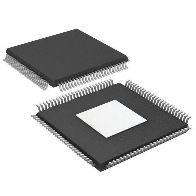
| 产品图片 |
|
| rohs | 符合RoHS无铅 / 符合限制有害物质指令(RoHS)规范要求 |
| 产品系列 | 数据转换器IC,数模转换器- DAC,Analog Devices AD5410AREZ- |
| 数据手册 | |
| 产品型号 | AD5410AREZ |
| 产品培训模块 | http://www.digikey.cn/PTM/IndividualPTM.page?site=cn&lang=zhs&ptm=19145http://www.digikey.cn/PTM/IndividualPTM.page?site=cn&lang=zhs&ptm=18614http://www.digikey.cn/PTM/IndividualPTM.page?site=cn&lang=zhs&ptm=24843http://www.digikey.cn/PTM/IndividualPTM.page?site=cn&lang=zhs&ptm=26125http://www.digikey.cn/PTM/IndividualPTM.page?site=cn&lang=zhs&ptm=26140http://www.digikey.cn/PTM/IndividualPTM.page?site=cn&lang=zhs&ptm=26150http://www.digikey.cn/PTM/IndividualPTM.page?site=cn&lang=zhs&ptm=26147 |
| 产品目录页面 | |
| 产品种类 | 数模转换器- DAC |
| 位数 | 12 |
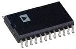
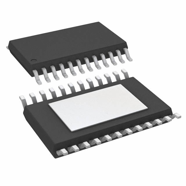
| 供应商器件封装 | 24-TSSOP-EP |
| 分辨率 | 12 bit |
| 包装 | 管件 |
| 商标 | Analog Devices |
| 安装类型 | 表面贴装 |
| 安装风格 | SMD/SMT |
| 封装 | Tube |
| 封装/外壳 | 24-TSSOP(0.173",4.40mm 宽)裸焊盘 |
| 封装/箱体 | TSSOP-24 |
| 工作温度 | -40°C ~ 85°C |
| 工厂包装数量 | 62 |
| 建立时间 | 40µs |
| 接口类型 | SPI |
| 数据接口 | DSP,MICROWIRE™,QSPI™,串行,SPI™ |
| 最大工作温度 | + 85 C |
| 最小工作温度 | - 40 C |
| 标准包装 | 62 |
| 电压参考 | Internal, External |
| 电压源 | 模拟和数字 |
| 电源电压-最大 | 26.4 V |
| 电源电压-最小 | 10.8 V |
| 积分非线性 | +/- 0.032 % FSR |
| 稳定时间 | 40 us |
| 系列 | AD5410 |
| 结构 | Segment |
| 设计资源 | |
| 转换器数 | 1 |
| 转换器数量 | 1 |
| 输出数和类型 | 1 电流,单极 |
| 输出类型 | Current |
| 采样率(每秒) | - |


- 商务部:美国ITC正式对集成电路等产品启动337调查
- 曝三星4nm工艺存在良率问题 高通将骁龙8 Gen1或转产台积电
- 太阳诱电将投资9.5亿元在常州建新厂生产MLCC 预计2023年完工
- 英特尔发布欧洲新工厂建设计划 深化IDM 2.0 战略
- 台积电先进制程称霸业界 有大客户加持明年业绩稳了
- 达到5530亿美元!SIA预计今年全球半导体销售额将创下新高
- 英特尔拟将自动驾驶子公司Mobileye上市 估值或超500亿美元
- 三星加码芯片和SET,合并消费电子和移动部门,撤换高东真等 CEO
- 三星电子宣布重大人事变动 还合并消费电子和移动部门
- 海关总署:前11个月进口集成电路产品价值2.52万亿元 增长14.8%


PDF Datasheet 数据手册内容提取
Single-Channel, 12-/16-Bit, Serial Input, 4 mA to 20 mA, Current Source DAC, HART Connectivity Data Sheet AD5410/AD5420 FEATURES GENERAL DESCRIPTION 12-/16-bit resolution and monotonicity The AD5410/AD5420 are low cost, precision, fully integrated Current output ranges: 4 mA to 20 mA, 0 mA to 20 mA, or 12-/16-bit converters offering a programmable current source 0 mA to 24 mA output designed to meet the requirements of industrial process ±0.01% FSR typical total unadjusted error (TUE) control applications. The output current range is programmable ±3 ppm/°C typical output drift at 4 mA to 20 mA, 0 mA to 20 mA, or an overrange function of Flexible serial digital interface 0 mA to 24 mA. The output is open-circuit protected. The device On-chip output fault detection operates with a power supply (AVDD) range from 10.8 V to On-chip reference (10 ppm/°C maximum) 60 V. Output loop compliance is 0 V to AV − 2.5 V. DD Feedback/monitoring of output current The flexible serial interface is SPI, MICROWIRE™, QSPI™, and Asynchronous clear function DSP compatible and can be operated in 3-wire mode to mini- Power supply (AV ) range DD mize the digital isolation required in isolated applications. 10.8 V to 40 V; AD5410AREZ/AD5420AREZ 10.8 V to 60 V; AD5410ACPZ/AD5420ACPZ The device also includes a power-on reset function, ensuring Output loop compliance to AV − 2.5 V that the device powers up in a known state, and an asynchronous DD Temperature range: −40°C to +85°C CLEAR pin that sets the output to the low end of the selected 24-lead TSSOP and 40-lead LFCSP packages current range. APPLICATIONS The total unadjusted error is typically ±0.01% FSR. COMPANION PRODUCTS Process control Actuator control HART Modem: AD5700, AD5700-1 PLC HART network connectivity FUNCTIONAL BLOCK DIAGRAM DVCC SELECT DVCC CAP1 CAP2 AVDD AD5410/AD5420 R3SENSE R2 R3 CLEAR BOOST LATCH INPUT SHIFT IOUT SCLK REGISTER 12/16 12-/16-BIT SDIN AND CONTROL DAC SDO LOGIC FAULT POWER- RSET ON VREF RESET RSET REFOUT REFIN GND 07027-001 Figure 1. Rev. J Document Feedback Information furnished by Analog Devices is believed to be accurate and reliable. However, no responsibility is assumed by Analog Devices for its use, nor for any infringements of patents or other One Technology Way, P.O. Box 9106, Norwood, MA 02062-9106, U.S.A. rights of third parties that may result from its use. Specifications subject to change without notice. No license is granted by implication or otherwise under any patent or patent rights of Analog Devices. Tel: 781.329.4700 ©2009–2017 Analog Devices, Inc. All rights reserved. Trademarks and registered trademarks are the property of their respective owners. Technical Support www.analog.com
AD5410/AD5420 Data Sheet TABLE OF CONTENTS Features .............................................................................................. 1 AD5410/AD5420 Features ............................................................ 22 Applications ....................................................................................... 1 Fault Alert .................................................................................... 22 General Description ......................................................................... 1 Asynchronous Clear (CLEAR) ................................................. 22 Companion Products ....................................................................... 1 Internal Reference ...................................................................... 22 Functional Block Diagram .............................................................. 1 External Current Setting Resistor ............................................ 22 Revision History ............................................................................... 3 Digital Power Supply .................................................................. 22 Specifications ..................................................................................... 4 External Boost Function ........................................................... 22 AC Performance Characteristics ................................................ 6 HART Communication ............................................................. 23 Timing Characteristics ................................................................ 6 Digital Slew Rate Control .......................................................... 23 Absolute Maximum Ratings ............................................................ 8 I Filtering Capacitors ............................................................ 25 OUT ESD Caution .................................................................................. 8 Feedback/Monitoring of Output Current ............................... 25 Pin Configurations and Function Descriptions ........................... 9 Applications Information .............................................................. 27 Typical Performance Characteristics ........................................... 11 Driving Inductive Loads ............................................................ 27 Terminology .................................................................................... 16 Transient Voltage Protection .................................................... 27 Theory of Operation ...................................................................... 17 Layout Guidelines....................................................................... 27 Architecture ................................................................................. 17 Galvanically Isolated Interface ................................................. 27 Serial Interface ............................................................................ 17 Microprocessor Interfacing ....................................................... 28 Power-On State ........................................................................... 20 Thermal and Supply Considerations ....................................... 28 Transfer Function ....................................................................... 20 Industrial, HART Compatible Analog Output Application . 29 Data Register ............................................................................... 20 Outline Dimensions ....................................................................... 30 Control Register .......................................................................... 20 Ordering Guide .......................................................................... 30 Reset Register .............................................................................. 21 Status Register ............................................................................. 21 Rev. J | Page 2 of 30
Data Sheet AD5410/AD5420 REVISION HISTORY 11/2017—Rev. I to Rev. J 11/2011—Rev. B to Rev. C Changes to Figure 6 ........................................................................... 9 Changes to Table 10 ........................................................................ 18 Updated Outline Dimensions ........................................................ 30 Changes to Ordering Guide ........................................................... 30 2/2010—Rev. A to Rev. B Changes to Figure 46 ..................................................................... 23 4/2017—Rev. H to Rev. I Changes to Table 4 ............................................................................ 8 8/2009—Rev. 0 to Rev. A Changes to Figure 5 and Figure 6 .................................................... 9 Changes to Features and General Description ............................. 1 Changes to Table 1 ............................................................................ 3 4/2015—Rev. G to Rev. H Changes to Table 2 ............................................................................ 5 Changes to Table 3 ............................................................................ 6 Changes to Introduction to Table 4 and to Table 4 ...................... 7 Changes to Table 5 ............................................................................ 9 Added Figure 6, Changes to Figure 5 and Table 5 ........................ 8 Added Feedback/Monitoring of Output Current Section, 10/2014—Rev. F to Rev. G Including Figure 45 to Figure 47; Renumbered Subsequent Changes to Power-On State Section ............................................. 20 Figures .............................................................................................. 23 Changes to Thermal and Supply Considerations Section and 10/2013—Rev. E to Rev. F Table 21 ............................................................................................. 26 Moved Revision History ................................................................... 3 Updated Outline Dimensions ........................................................ 28 Changes to Figure 51 ...................................................................... 27 Changes to Ordering Guide ........................................................... 28 Changes to Figure 55 ...................................................................... 29 3/2009—Revision 0: Initial Version 3/2013—Rev. D to Rev. E Changes to Table 4 ............................................................................ 7 Added Figure 40, Renumbered Sequentially ............................... 19 Changes to Table 10 ........................................................................ 20 Changes to Thermal and Supply Considerations Section and Table 21 ..................................................................................... 27 Updated Outline Dimensions ........................................................ 29 5/2012—Rev. C to Rev. D Reorganized Layout ........................................................... Universal Changes to Product Title .................................................................. 1 Added Companion Products Section; Changes to Features Section and Applications Section .................................................... 1 Changes to Table 5 ............................................................................ 9 Change to Figure 8 .......................................................................... 11 Added HART Communication Section and Figure 41, Renumbered Sequentially .............................................................. 21 Changes to Industrial, HART Compatible Analog Output Application Section and Figure 54 ................................................ 27 Rev. J | Page 3 of 30
AD5410/AD5420 Data Sheet SPECIFICATIONS AV = 10.8 V to 26.4 V, GND = 0 V, REFIN = 5 V external; DV = 2.7 V to 5.5 V, R = 300 Ω; all specifications T to T , DD CC LOAD MIN MAX unless otherwise noted. Table 1. Parameter1 Min Typ Max Unit Test Conditions/Comments OUTPUT CURRENT RANGES 0 24 mA 0 20 mA 4 20 mA ACCURACY, INTERNAL R SET Resolution 16 Bits AD5420 12 Bits AD5410 Total Unadjusted Error (TUE) −0.3 +0.3 % FSR AD5420 −0.13 ±0.08 +0.13 % FSR AD5420, T = 25°C A −0.5 +0.5 % FSR AD5410 −0.3 ±0.15 +0.3 % FSR AD5410, T = 25°C A Relative Accuracy (INL)2 −0.024 +0.024 % FSR AD5420 −0.032 +0.032 % FSR AD5410 Differential Nonlinearity (DNL) −1 +1 LSB Guaranteed monotonic Offset Error −0.27 +0.27 % FSR −0.12 ±0.08 +0.12 % FSR T = 25°C A Offset Error Temperature Coefficient (TC)3 ±16 ppm FSR/°C Gain Error −0.18 +0.18 % FSR AD5420 −0.03 ±0.006 +0.03 % FSR AD5420, T = 25°C A −0.22 +0.22 AD5410 −0.06 ±0.012 +0.06 AD5410, T = 25°C A Gain Error Temperature Coefficient (TC)3 ±10 ppm FSR/°C Full-Scale Error −0.2 +0.2 % FSR −0.1 ±0.08 +0.1 % FSR T = 25°C A Full-Scale Error Temperature Coefficient (TC)3 ±12 ppm FSR/°C ACCURACY, EXTERNAL R Assumes an ideal 15 kΩ resistor SET Resolution 16 Bits AD5420 12 Bits AD5410 Total Unadjusted Error (TUE) −0.15 +0.15 % FSR AD5420 −0.06 ±0.01 +0.06 % FSR AD5420, T = 25°C A −0.3 +0.3 % FSR AD5410 −0.1 ±0.02 +0.1 % FSR AD5410, TA = 25°C Relative Accuracy (INL)2 −0.012 +0.012 % FSR AD5420 −0.032 +0.032 % FSR AD5410 Differential Nonlinearity (DNL) −1 +1 LSB Guaranteed monotonic Offset Error −0.1 +0.1 % FSR −0.03 ±0.006 +0.03 % FSR T = 25°C A Offset Error Temperature Coefficient (TC)3 ±3 ppm FSR/°C Gain Error −0.08 +0.08 % FSR −0.05 ±0.003 +0.05 % FSR T = 25°C A Gain Error Temperature Coefficient (TC)3 ±4 ppm FSR/°C Full-Scale Error −0.15 +0.15 % FSR −0.06 ±0.01 +0.06 % FSR T = 25°C A Full-Scale Error Temperature Coefficient (TC)3 ±7 ppm FSR/°C OUTPUT CHARACTERISTICS3 Current Loop Compliance Voltage 0 AV − 2.5 V DD Output Current Drift vs. Time 50 ppm FSR Internal R , drift after 1000 hours at 125°C SET 20 ppm FSR External R , drift after 1000 hours at 125°C SET Resistive Load 1200 Ω Inductive Load 50 mH T = 25°C A DC Power Supply Rejection Ratio (PSRR) 1 µA/V Rev. J | Page 4 of 30
Data Sheet AD5410/AD5420 Parameter1 Min Typ Max Unit Test Conditions/Comments Output Impedance 50 MΩ Output Current Leakage 60 pA Output disabled R3 Resistor Value 36 40 44 Ω T = 25°C A R3 Resistor Temperature Coefficient (TC) 30 ppm/°C I Current 399 444 489 µA BIAS I Current Temperature Coefficient (TC) 30 ppm/°C BIAS REFERENCE INPUT/OUTPUT Reference Input3 Reference Input Voltage 4.95 5 5.05 V For specified performance DC Input Impedance 25 30 kΩ Reference Output Output Voltage 4.995 5.000 5.005 V T = 25°C A Reference TC3, 4 1.8 10 ppm/°C Output Noise (0.1 Hz to 10 Hz)3 18 µV p-p Noise Spectral Density3 100 nV/√Hz At 10 kHz Output Voltage Drift vs. Time3 50 ppm Drift after 1000 hours, TA = 125°C Capacitive Load3 600 nF Load Current3 5 mA Short-Circuit Current3 7 mA Load Regulation3 95 ppm/mA DIGITAL INPUTS3 JEDEC compliant Input High Voltage, V 2 V IH Input Low Voltage, V 0.8 V IL Input Current −1 +1 µA Per pin Pin Capacitance 10 pF Per pin DIGITAL OUTPUTS3 SDO Output Low Voltage, V 0.4 V Sinking 200 µA OL Output High Voltage, V DV − 0.5 V Sourcing 200 µA OH CC High Impedance Leakage Current −1 +1 µA High Impedance Output Capacitance 5 pF FAULT Output Low Voltage, V 0.4 V 10 kΩ pull-up resistor to DV OL CC Output Low Voltage, V 0.6 V 2.5 mA load current OL Output High Voltage, V 3.6 V 10 kΩ pull-up resistor to DV OH CC POWER REQUIREMENTS AV 10.8 40 V TSSOP package DD 10.8 60 V LFCSP package DV CC Input Voltage 2.7 5.5 V Internal supply disabled Output Voltage 4.5 V DV can be overdriven up to 5.5 V CC Output Load Current3 5 mA Short-Circuit Current3 20 mA AI 3 mA Output disabled DD 4 mA Output enabled DI 1 mA V = DV , V = GND CC IH CC IL Power Dissipation 144 mW AV = 40 V, I = 0 mA DD OUT 50 mW AV = 15 V, I = 0 mA DD OUT 1 Temperature range: −40°C to +85°C; typical at +25°C. 2 For 0 mA to 20 mA and 0 mA to 24 mA ranges, INL is measured from Code 256 for the AD5420 and Code 16 for the AD5410. 3 Guaranteed by design and characterization but not production tested. 4 The on-chip reference is production trimmed and tested at 25°C and 85°C. It is characterized from −40°C to +85°C. Rev. J | Page 5 of 30
AD5410/AD5420 Data Sheet AC PERFORMANCE CHARACTERISTICS AV = 10.8 V to 26.4 V, GND = 0 V, REFIN = 5 V external; DV = 2.7 V to 5.5 V, R = 300 Ω; all specifications T to T , unless DD CC LOAD MIN MAX otherwise noted. Table 2. Parameter1 Min Typ Max Unit Test Conditions/Comments DYNAMIC PERFORMANCE Output Current Settling Time2 10 µs 16 mA step, to 0.1% FSR 40 µs 16 mA step, to 0.1% FSR, L = 1 mH AC PSRR −75 dB 200 mV, 50 Hz/60 Hz sine wave superimposed on power supply voltage 1 Guaranteed by design and characterization; not production tested. 2 Digital slew rate control feature disabled and CAP1 = CAP2 = open circuit. TIMING CHARACTERISTICS AV = 10.8 V to 26.4 V, GND = 0 V, REFIN = 5 V external; DV = 2.7 V to 5.5 V, R = 300 Ω; all specifications T to T , unless DD CC LOAD MIN MAX otherwise noted. Table 3. Parameter1, 2, 3 Limit at T , T Unit Description MIN MAX WRITE MODE t 33 ns min SCLK cycle time 1 t 13 ns min SCLK low time 2 t 13 ns min SCLK high time 3 t 13 ns min LATCH delay time 4 t 5 µs min LATCH high time 5 t 5 ns min Data setup time 6 t 5 ns min Data hold time 7 t 40 ns min LATCH low time 8 t 20 ns min CLEAR pulse width 9 t 5 µs max CLEAR activation time 10 READBACK MODE t 90 ns min SCLK cycle time 11 t 40 ns min SCLK low time 12 t 40 ns min SCLK high time 13 t 13 ns min LATCH delay time 14 t 40 ns min LATCH high time 15 t 5 ns min Data setup time 16 t 5 ns min Data hold time 17 t 40 ns min LATCH low time 18 t 35 ns max Serial output delay time (C = 50 pF)4 19 L SDO t 35 ns max LATCH rising edge to SDO tristate 20 DAISY-CHAIN MODE t 90 ns min SCLK cycle time 21 t 40 ns min SCLK low time 22 t 40 ns min SCLK high time 23 t 13 ns min LATCH delay time 24 t 40 ns min LATCH high time 25 t 5 ns min Data setup time 26 t 5 ns min Data hold time 27 t 40 ns min LATCH low time 28 t 35 ns max Serial output delay time (C = 50 pF)4 29 L SDO 1 Guaranteed by characterization but not production tested. 2 All input signals are specified with tR = tF = 5 ns (10% to 90% of DVCC) and timed from a voltage level of 1.2 V. 3 See Figure 2, Figure 3, and Figure 4. 4 CLSDO = capacitive load on SDO output. Rev. J | Page 6 of 30
Data Sheet AD5410/AD5420 t1 SCLK 1 2 24 t2 t3 t4 t5 LATCH t7 t8 t6 SDIN DB23 DB0 t9 CLEAR t10 IOUT 07027-002 Figure 2. Write Mode Timing Diagram t11 SCLK 1 2 24 1 2 8 9 22 23 24 t12 t13 t14 t15 LATCH t17 t18 t16 SDIN DB23 DB0 DB23 DB0 INPUT WORD SPECIFIES NOP CONDITION REGISTER TO BE READ t19 t20 SDO X X X X DB15 DB0 UNDEFINED DATA FDIORNS’TT 8C BAIRTES BAIRTES SDEALTEAC CTLEODC RKEEGDI SOTUETR 07027-003 Figure 3. Readback Mode Timing Diagram t21 SCLK 1 2 24 25 26 48 t22 t23 t24 t25 LATCH t27 t28 t26 SDIN DB23 DB0 DB23 DB0 INPUTWORDFORDACN t29 INPUTWORDFORDACN – 1 SDO DB23 UNDEFINED DB0 DB23 INPUTWORDFORDACN DB0 07027-004 Figure 4. Daisy-Chain Mode Timing Diagram Rev. J | Page 7 of 30
AD5410/AD5420 Data Sheet ABSOLUTE MAXIMUM RATINGS T = 25°C, unless otherwise noted. Transient currents of up to Stresses at or above those listed under Absolute Maximum A 80 mA do not cause SCR latch-up. Ratings may cause permanent damage to the product. This is a stress rating only; functional operation of the product at these Table 4. or any other conditions above those indicated in the operational Parameter Rating section of this specification is not implied. Operation beyond AV to GND −0.3 V to +60 V DD the maximum operating conditions for extended periods may DV to GND −0.3 V to +7 V CC affect product reliability. Digital Inputs to GND −0.3 V to DV + 0.3 V or +7 V CC (whichever is less) Digital Outputs to GND −0.3 V to DV + 0.3 V or +7 V ESD CAUTION CC (whichever is less) REFIN, REFOUT to GND −0.3 V to +7 V I to GND −0.3 V to AV OUT DD Operating Temperature Range Industrial −40°C to +85°C1 Storage Temperature Range −65°C to +150°C Junction Temperature (T max) 125°C J 24-Lead TSSOP_EP Package Thermal Impedance, θ 35°C/W2 JA Thermal Impedance, θ 9°C/W JC 40-Lead LFCSP Package Thermal Impedance, θ 33°C/W2 JA Thermal Impedance, θ 4°C/W JC Power Dissipation (T max − T )/θ J A JA Lead Temperature JEDEC industry standard Soldering J-STD-020 1 Power dissipated on chip must be derated to keep junction temperature below 125°C. The assumption is that the maximum power dissipation condition is sourcing 24 mA into ground from AVDD with a 4 mA on-chip current. 2 Thermal impedance simulated values are based on JEDEC 2S2P thermal test board with thermal vias. Ref: JEDEC JESD51 documents. Rev. J | Page 8 of 30
Data Sheet AD5410/AD5420 PIN CONFIGURATIONS AND FUNCTION DESCRIPTIONS GND 1 24 AVDD CNVDCCCNDNGVADDCNCNCNCNCN 0987654321 DVCC 2 23 NC 4333333333 FAULT 3 22 CAP2 GND 4 21 CAP1 NC 1 30 NC FAULT 2 29 CAP2 GND 5 20 BOOST GND 3 28 CAP1 AD5410/ GND 4 AD5410/AD5420 27 BOOST CLLAETACRH 67 (NAToOtD Pto5 V 4SIE2cWa0le) 1198 RIO3USTENSE CLALSECTACLRKH 567 (NToOt Pto V SIEcaWle) 222456 NRIOC3USTENSE SCLK 8 17 NC SDIN 8 23 DVCC SELECT SDO 9 22 NC SDIN 9 16 DVCC SELECT NC10 21 NC SDO 10 15 REFIN GND 11 14 REFOUT 11213141516171819102 GND 12 13 RSET CNDNGDNGDNGDNGRTESTUONIFECNCN FER R NOTES NOTES 12 .. NTTHHCEE = EGNXROPO OCUOSNENDDN R EPECAFTDE. RMEUNSCTE B.E CONNECTED TO 07027-005 12 .. NTTHHCEE = EGNXROPO OCUOSNENDDN R EPECAFTDE. RMEUNSCTE B.E CONNECTED TO 07027-053 Figure 5. TSSOP Pin Configuration Figure 6. LFCSP Pin Configuration Table 5. Pin Function Descriptions TSSOP Pin No. LFCSP Pin No. Mnemonic Description 1, 4, 5, 11, 12 3, 4, 12 to 15, 37 GND Ground Reference Pin. These pins must be connected to ground. 2 39 DV Digital Supply Pin. Voltage ranges from 2.7 V to 5.5 V. CC 3 2 FAULT Fault Alert. This pin is asserted low when an open circuit is detected between I and OUT GND or an overtemperature is detected. The FAULT pin is an open-drain output and must be connected to DV through a pull-up resistor (typically 10 kΩ). CC 6 5 CLEAR Active High Input. Asserting this pin sets the output current to the zero-scale value, which is either 0 mA or 4 mA, depending on the output range programmed, that is, 0 mA to 20 mA, 0 mA to 24 mA, or 4 mA to 20 mA. 7 6 LATCH Positive Edge Sensitive Latch. A rising edge parallel loads the input shift register data into the relevant register. In the case of the data register, the output current is also updated. 8 7 SCLK Serial Clock Input. Data is clocked into the input shift register on the rising edge of SCLK. This operates at clock speeds of up to 30 MHz. 9 8 SDIN Serial Data Input. Data must be valid on the rising edge of SCLK. 10 9 SDO Serial Data Output. This pin is used to clock data from the device in daisy-chain or readback mode. Data is clocked out on the falling edge of SCLK. See Figure 3 and Figure 4. 13 16 R An external, precision, low drift 15 kΩ current setting resistor can be connected to this SET pin to improve the overall performance of the device. See the Specifications and AD5410/AD5420 Features sections. 14 17 REFOUT Internal Reference Voltage Output. V = 5 V ± 5 mV at T = 25°C. Typical temperature REFOUT A drift is 1.8 ppm/°C. 15 18 REFIN External Reference Voltage Input. V = 5 V ± 50 mV for specified performance. REFIN 16 23 DV This pin, when connected to GND, disables the internal supply, and an external supply CC SELECT must be connected to the DV pin. Leave this pin unconnected to enable the internal CC supply. In this case, it is recommended to connect a 0.1 μF capacitor between DV and CC GND. See the AD5410/AD5420 Features section. 17, 23 1, 10, 11, 19 to NC Do not connect to these pins. 22, 24, 30 to 35, 38, 40 Rev. J | Page 9 of 30
AD5410/AD5420 Data Sheet TSSOP Pin No. LFCSP Pin No. Mnemonic Description 18 25 R3 The voltage measured between this pin and the BOOST pin is directly proportional to SENSE the output current and can be used as a monitor/feedback feature. This should be used as a voltage sense output only; current should not be sourced from this pin. See the AD5410/AD5420 Features section. 19 26 I Current Output Pin. OUT 20 27 BOOST Optional External Transistor Connection. Connecting an external transistor reduces the power dissipated in the AD5410/AD5420. See the AD5410/AD5420 Features section. 21 28 CAP1 Connection for Optional Output Filtering Capacitor. See the AD5410/AD5420 Features section. 22 29 CAP2 Connection for Optional Output Filtering Capacitor. See the AD5410/AD5420 Features section. Also HART Input Connection, see Device Features Section. 24 36 AV Positive Analog Supply Pin. Voltage ranges from 10.8 V to 40 V. DD 25 (EPAD) 41 (EPAD) Exposed pad The exposed pad must be connected to the ground reference. Rev. J | Page 10 of 30
Data Sheet AD5410/AD5420 TYPICAL PERFORMANCE CHARACTERISTICS 0.004 0.004 EXTERNAL RSET AVDD = 24V IENXTTEERRNNAALL R RSSEETT, BOOST TRANSISTOR 0.002 0mA TO 24mA RANGE 0.002 INTERNAL RSET, BOOST TRANSISTOR 0 R) 0 R) S S F F % % –0.002 R ( –0.002 R ( O O ERR –0.004 ERR –0.004 L L N N I –0.006 I –0.006 AVDD = 2.4V ––00..001008 TRAL O=A 2D5 =°C 250Ω 07027-006 ––00..001008 07027-009 0 10,000 20,000 30,000 40,000 50,000 60,000 –40 –20 0 20 40 60 80 CODE TEMPERATURE (°C) Figure 7. Integral Nonlinearity Error vs. Code Figure 10. Integral Nonlinearity Error vs. Temperature, Internal RSET 1.0 0.003 AVDD = 24V AVDD = 24V 0.8 TA = 25°C 0mA TO 24mA RANGE RLOAD = 250Ω 0.002 0.6 B) 0.4 SR) 0.001 ROR (LS 0.02 OR (% F 0 R R DNL E ––00..24 INL ER –0.001 –0.6 EXTERNAL RSET INTERNAL RSET –0.002 ––10..08 IENXTTEERRNNAALL R RSSEETT, ,B BOOOOSSTT T TRRAANNSSISISTTOORR 07027-007 –0.003 07027-109 0 10,000 20,000 30,000 40,000 50,000 60,000 –40 –20 0 20 40 60 80 CODE TEMPERATURE (°C) Figure 8. Differential Nonlinearity Error vs. Code Figure 11. Integral Nonlinearity Error vs. Temperature, External RSET 0.05 1.0 AVDD = 24V 0.03 0.8 ALL RANGES SR) INTERNAL AND EXTERNAL RSET F 0.01 0.6 % R ( –0.01 0.4 O B) RR –0.03 LS 0.2 TED E –0.05 AVDD = 24V ROR ( 0 UNADJUS ––00..0097 RTALO=A 2D5 =°C 250Ω DNL ER ––00..42 OTAL –0.11 EINXTTEERRNNAALL R RSSEETT –0.6 T ––00..1153 IENXTTEERRNNAALL R RSSEETT, ,B BOOOOSSTT T TRRAANNSSISISTTOORR 07027-008 ––10..08 07027-010 0 10,000 20,000 30,000 40,000 50,000 60,000 –40 –20 0 20 40 60 80 CODE TEMPERATURE (°C) Figure 9. Total Unadjusted Error vs. Code Figure 12. Differential Nonlinearity Error vs. Temperature Rev. J | Page 11 of 30
AD5410/AD5420 Data Sheet 0.10 0.015 TA = 25°C 0mA TO 24mA RANGE SR) 0.05 AVDD = 24V 0.010 F % USTED ERROR ( ––00..10050 RROR (% FSR) 0.0050 ADJ 4mA TO 20mA INTERNAL RSET NL E–0.005 UN –0.15 0mA TO 20mA INTERNAL RSET I AL 0mA TO 24mA INTERNAL RSET TOT ––00..2250 400mmmAAA TTTOOO 222004mmmAAA EEEXXXTTTEEERRRNNNAAALLL RRRSSSEEETTT 07027-013 ––00..001150 07027-011 –40 –20 0 20 40 60 80 10 15 20 25 30 35 40 TEMPERATURE (°C) AVDD (V) Figure 13. Total Unadjusted Error vs. Temperature Figure 16. Integral Nonlinearity Error vs. AVDD, External RSET 0.10 0.020 0.015 0.05 AVDD = 24V TA = 25°C 0mA TO 24mA RANGE % FSR) 0 FSR) 00..000150 OR ( –0.05 R (% R O 0 R R T E –0.10 ER OFFSE –0.15 400mmmAAA TTTOOO 222004mmmAAA IIINNNTTTEEERRRNNNAAALLL RRRSSSEEETTT INL ––00..001005 4mA TO 20mA EXTERNAL RSET ––00..2250 00mmAA TTOO 2204mmAA EEXXTTEERRNNAALL RRSSEETT 07027-017 ––00..001250 07027-014 –40 –20 0 20 40 60 80 10 15 20 25 30 35 40 TEMPERATURE (°C) AVDD (V) Figure 14. Offset Error vs. Temperature Figure 17. Integral Nonlinearity Error vs. AVDD, Internal RSET 0.06 1.0 0.8 TA = 25°C 0.04 AVDD = 24V 0mA TO 24mA RANGE 0.6 0.02 SR) B) 0.4 % F 0 (LS 0.2 OR ( –0.02 ROR 0 R R R E GAIN E –0.04 40mmAA TTOO 2200mmAA IINNTTEERRNNAALL RRSSEETT DNL––00..42 –0.06 0mA TO 24mA INTERNAL RSET –0.6 4mA TO 20mA EXTERNAL RSET ––00..1008 00mmAA TTOO 2204mmAA EEXXTTEERRNNAALL RRSSEETT 07027-018 ––10..08 07027-012 –40 –20 0 20 40 60 80 10 15 20 25 30 35 40 TEMPERATURE (°C) AVDD(V) Figure 15. Gain Error vs. Temperature Figure 18. Differential Nonlinearity Error vs. AVDD, External RSET Rev. J | Page 12 of 30
Data Sheet AD5410/AD5420 1.0 2.5 AVDD = 15V 00..86 0TmA A= 2T5O° C24mA RANGE 2.0 RIOLUOTA =D 2=4 5m0A0Ω V) 0.4 ( B) GE RROR (LS 0.02 M VOLTA 1.5 L E –0.2 OO 1.0 N R D D –0.4 A E H –0.6 0.5 ––01..80 07027-015 0 07027-019 10 15 20 25 30 35 40 –40 –20 0 20 40 60 80 AVDD (V) TEMPERATURE (°C) Figure 19. Differential Nonlinearity Error vs. AVDD, Internal RSET Figure 22. Compliance Voltage Headroom vs. Temperature 0.025 3.5 SR) 0.020 0TmA A= 2T5O° C24mA RANGE 3.0 ATAV D=D 2 =5 °2C4V % F 0.015 RLOAD = 250Ω R ( 2.5 RO 0.010 A) R µ D E NT( 2.0 DJUSTE 0.0050 CURRE 1.5 NA UT U P AL –0.005 UT 1.0 T O O T––00..00110510 15 20 25 30 35 40 07027-016 0.05 07027-020 0 100 200 300 400 500 600 AVDD (V) TIME (µs) Figure 20. Total Unadjusted Error vs. AVDD, External RSET Figure 23. Output Current vs. Time on Power-Up 0.05 20 0.03 R) 10 FS 0.01 % TED ERROR( –––000...000531 T0mA A= T2O5° C24mA RANGE URRENT (µA) –100 RATAVL OD=AD 2D =5 =° 2C 245V0Ω S C DJU –0.07 UT –20 A P L UN –0.09 OUT –30 TA –0.11 O T ––00..1153 07027-032 ––5400 07027-021 10 15 20 25 30 35 40 0 0.5 1.0 1.5 2.0 2.5 3.0 3.5 4.0 4.5 5.0 AVDD(V) TIME (µs) Figure 21. Total Unadjusted Error vs. AVDD, Internal RSET Figure 24. Output Current vs. Time on Output Enable Rev. J | Page 13 of 30
AD5410/AD5420 Data Sheet 900 800 TA = 25°C 700 AVDD 600 µA) 500 DVCC = 5V (C 3 DIC400 REFERENCE OUTPUT 300 200 1000 DVCC = 3V 07027-022 1 07027-025 0 0.5 1.0 1.5 2.0 2.5 3.0 3.5 4.0 4.5 5.0 CH1 2.00V M200µs CH3 2.1V LOGIC VOLTAGE (V) CH3 5.00V Figure 25. DICC vs. Logic Input Voltage Figure 28. Reference Turn-on Transient 5.0 4.5 TIOAU =T =2 50°mCA 4.0 3.5 A)3.0 m (D2.5 1 D AI2.0 1.5 1.0 0.50 07027-023 07027-026 10 15 20 25 30 35 40 CH1 2µV M2.00s LINE 1.8V AVDD (V) Figure 26. AIDD vs. AVDD Figure 29. Reference Noise (0.1 Hz to 10 Hz Bandwidth) 9 TA = 25°C 8 V) 7 E ( AG 6 T L O 5 V UT 1 P 4 T U O 3 C C V D 2 01 07027-024 07027-027 –21 –19 –17 –15 –13 –11 –9 –7 –5 –3 –1 1 CH1 20µV M2.00s LINE 0V LOAD CURRENT (mA) Figure 27. DVCC Output Voltage vs. Load Current Figure 30. Reference Noise (100 kHz Bandwidth) Rev. J | Page 14 of 30
Data Sheet AD5410/AD5420 70 5.0005 5.0000 TA = 25°C 60 V) AVDD = 24V E (4.9995 RENT (pA) 4500 T VOLTAG44..99998950 R U LEAKAGE CU 123000 ATAV D=D 2 =5° 4C0V ERENCE OUTP444...999999778050 OUTPUT DISABLED EF4.9965 R –100 07027-028 44..99995650 07027-031 0 5 10 15 20 25 30 35 40 45 0 1 2 3 4 5 6 7 8 9 COMPLIANCE VOLTAGE (V) LOAD CURRENT (mA) Figure 31. Output Leakage Current vs. Compliance Voltage Figure 34. Reference Output Voltage vs. Load Current 5.003 30 E (V)5.002 5A0V DDDE V=I C24EVS SHOWN 20 ATRAVL OD=AD 2D =5 =° 2C 245V0Ω 00xx870F0F0F TTOO 00xx78F0F0F0 G A A) OLT5.001 T (µ 10 V N UT RE TP5.000 UR 0 U C O T RENCE 4.999 OUTPU–10 E F RE4.998 –20 4.997 07027-029 –30 07027-049 –40 –20 0 20 40 60 80 0 2 4 6 8 10 12 14 16 18 20 TEMPERATURE (°C) TIME (µs) Figure 32. Reference Output Voltage vs. Temperature Figure 35. Digital-to-Analog Glitch 45 25 40 AVDD = 24V TA = 25°C 35 20 AVDD = 24V A) RLOAD = 300Ω N(%)30 NT (m15 OPULATIO2205 UT CURRE10 P15 TP U O 10 5 05 07027-030 0 07027-134 0 1 2 3 4 5 6 7 8 9 10 –1 0 1 2 3 4 5 6 7 8 TEMPERATURE COEFFICIENT (ppm/°C) TIME (µs) Figure 33. Reference Temperature Coefficient Histogram Figure 36. 4 mA to 20 mA Output Current Step Rev. J | Page 15 of 30
AD5410/AD5420 Data Sheet TERMINOLOGY Gain Error Temperature Coefficient (TC) Relative Accuracy or Integral Nonlinearity (INL) This is a measure of the change in gain error with changes in For the DAC, relative accuracy, or integral nonlinearity (INL), is temperature. Gain error TC is expressed in ppm FSR/°C. a measure of the maximum deviation, in % FSR, from a straight line passing through the endpoints of the DAC transfer Current Loop Compliance Voltage function. A typical INL vs. code plot is shown in Figure 7. This is the maximum voltage at the I pin for which the OUT output current is equal to the programmed value. Differential Nonlinearity (DNL) Differential nonlinearity (DNL) is the difference between the Power Supply Rejection Ratio (PSRR) measured change and the ideal 1 LSB change between any two PSRR indicates how the output of the DAC is affected by adjacent codes. A specified differential nonlinearity of ±1 LSB changes in the power supply voltage. maximum ensures monotonicity. This DAC is guaranteed Voltage Reference Temperature Coefficient (TC) monotonic by design. A typical DNL vs. code plot can be seen Voltage reference TC is a measure of the change in the reference in Figure 8. output voltage with a change in temperature. The voltage Total Unadjusted Error (TUE) reference TC is calculated using the box method, which defines Total unadjusted error (TUE) is a measure of the output error the TC as the maximum change in the reference output over a taking all the various errors into account, namely INL error, given temperature range, expressed in ppm/°C as follows: offset error, gain error, and output drift over supplies and V −V temperature. TUE is expressed in % FSR. A typical TUE vs. TC= REFmax REFmin ×106 code plot can be seen in Figure 9. VREFnom×TempRange Monotonicity where: A DAC is monotonic if the output either increases or remains VREFmax is the maximum reference output measured over the constant for increasing digital input code. The AD5410/AD5420 total temperature range. are monotonic over their full operating temperature range. VREFmin is the minimum reference output measured over the total temperature range. Full-Scale Error V is the nominal reference output voltage, 5 V. Full-scale error is a measure of the output error when full-scale REFnom TempRange is the specified temperature range, −40°C to +85°C. code is loaded to the data register. Ideally, the output should be full-scale − 1 LSB. Full-scale error is expressed as a percentage Reference Load Regulation of the full-scale range (% FSR). Load regulation is the change in reference output voltage due to a specified change in load current. It is expressed in ppm/mA. Full-Scale Error Temperature Coefficient (TC) This is a measure of the change in full-scale error with changes in temperature. Full-scale error TC is expressed in ppm FSR/°C. Gain Error This is a measure of the span error of the DAC. It is the devia- tion in slope of the DAC transfer characteristic from the ideal expressed in % FSR. A plot of gain error vs. temperature can be seen in Figure 15. Rev. J | Page 16 of 30
Data Sheet AD5410/AD5420 THEORY OF OPERATION The AD5410/AD5420 are precision digital-to-current loop output SCLK. The input shift register consists of eight address bits and converters designed to meet the requirements of industrial 16 data bits, as shown in Table 6. The 24-bit word is uncondition- process control applications. They provide a high precision, ally latched on the rising edge of LATCH. Data continues to be fully integrated, low cost single-chip solution for generating clocked in irrespective of the state of LATCH. On the rising edge current loop outputs. The current ranges available are 0 mA of LATCH, the data that is present in the input shift register is to 20 mA, 0 mA to 24 mA, and 4 mA to 20 mA. The desired latched; that is, the last 24 bits to be clocked in before the rising output configuration is user selectable via the control register. edge of LATCH is the data that is latched. The timing diagram for this operation is shown in Figure 2. ARCHITECTURE Standalone Operation The DAC core architecture of the AD5410/AD5420 consists of two matched DAC sections. A simplified circuit diagram is shown The serial interface works with both a continuous and noncon- in Figure 37. The four MSBs of the 12-bit or 16-bit data-word tinuous SCLK. A continuous SCLK source can be used only if are decoded to drive 15 switches, E1 to E15. Each of these switches LATCH is taken high after the correct number of data bits has connects one of 15 matched resistors to either ground or the been clocked in. In gated clock mode, a burst clock containing reference buffer output. The remaining 8/12 bits of the data- the exact number of clock cycles must be used, and LATCH word drive Switch S0 to Switch S7 or Switch S0 to Switch S11 of an must be taken high after the final clock to latch the data. The 8-/12-bit voltage mode R-2R ladder network. first rising edge of SCLK that clocks in the MSB of the data- word marks the beginning of the write cycle. Exactly 24 rising VOUT clock edges must be applied to SCLK before LATCH is brought 2R 2R 2R 2R 2R 2R 2R high. If LATCH is brought high before the 24th rising SCLK S0 S1 S7/S11 E1 E2 E15 edge, the data written is invalid. If more than 24 rising SCLK VREFIN edges are applied before LATCH is brought high, the input data is also invalid. 8-/12-BIT R-2R LADDER FOU15R EMQSUBAsL D SEECGOMDEENDT ISNTO 07027-033 MTaSbBl e 6 . Input Shift Register Format LSB Figure 37. DAC Ladder Structure DB23 to DB16 DB15 to DB0 The voltage output from the DAC core is converted to a current Address byte Data-word (see Figure 38) that is then mirrored to the supply rail so that Table 7. Address Byte Functions the application simply sees a current source output with respect Address Byte Function to ground. 00000000 No operation (NOP) AVDD 00000001 Data register 00000010 Readback register value as per read address (see Table 8) R2 R3 01010101 Control register T2 01010110 Reset register A2 12-/16-BIT T1 IOUT Daisy-Chain Operation DAC A1 For systems that contain several devices, the SDO pin can be used to daisy-chain several devices together, as shown in Figure 39. RSET This daisy-chain mode can be useful in system diagnostics and 07027-034 mino rdede uisc iennga bthleed n buym sbeettri nogf stehrei aDl CinEteNrf bacite o lfin tehse. cDoanitsryo-lc hreaginis ter. Figure 38. Voltage-to-Current Conversion Circuitry The first rising edge of SCLK that clocks in the MSB of the data- SERIAL INTERFACE word marks the beginning of the write cycle. SCLK is continuously The AD5410/AD5420 are controlled over a versatile 3-wire applied to the input shift register. If more than 24 clock pulses serial interface that operates at clock rates of up to 30 MHz. They are applied, the data ripples out of the input shift register and are compatible with SPI, QSPI, MICROWIRE, and DSP appears on the SDO line. This data, having been clocked out on standards. the previous falling SCLK edge, is valid on the rising edge of SCLK. By connecting the SDO of the first device to the SDIN Input Shift Register input of the next device in the chain, a multidevice interface is The input shift register is 24 bits wide. Data is loaded into the constructed. Each device in the system requires 24 clock pulses. device MSB first as a 24-bit word under the control of a serial clock input, SCLK. Data is clocked in on the rising edge of Rev. J | Page 17 of 30
AD5410/AD5420 Data Sheet Therefore, the total number of clock cycles must equal 24 × N, Readback Operation where N is the total number of AD5410/AD5420 devices in the Readback mode is invoked by setting the address byte and read chain. When the serial transfer to all devices is complete, address as shown in Table 9 and Table 8 when writing to the LATCH is taken high. This latches the input data in each device input shift register. The next write to the AD5410/AD5420 in the daisy chain. The serial clock can be a continuous or a should be a NOP command, which clocks out the data from the gated clock. previously addressed register, as shown in Figure 3. By default, A continuous SCLK source can be used only if LATCH is taken the SDO pin is disabled. After having addressed the AD5410/ high after the correct number of clock cycles. In gated clock AD5420 for a read operation, a rising edge on LATCH enables mode, a burst clock containing the exact number of clock cycles the SDO pin in anticipation of data being clocked out. After the must be used, and LATCH must be taken high after the final data has been clocked out on SDO, a rising edge on LATCH clock to latch the data. See Figure 4 for a timing diagram. disables (tristate) the SDO pin once again. To read back the data register, for example, the following sequence should be CONTROLLER AD5410/ implemented: AD5420* DATA OUT SDIN 1. Write 0x020001 to the AD5410/AD5420 input shift SERIALCLOCK SCLK register. This configures the part for read mode with the CONTROL OUT LATCH data register selected. 2. Follow this with a second write, a NOP condition, 0x000000. DATA IN SDO During this write, the data from the data register is clocked out on the SDO line. SDIN AD5410/ Table 8. Read Address Decoding AD5420* Read Address Function SCLK 00 Read status register LATCH 01 Read data register 10 Read control register SDO SDIN AD5410/ AD5420* SCLK LATCH SDO *ADDITIONALPINS OMITTEDFORCLARITY. 07027-035 Figure 39. Daisy Chaining the AD5410/AD5420 Table 9. Input Shift Register Contents for a Read Operation MSB LSB DB23 DB22 DB21 DB20 DB19 DB18 DB17 DB16 DB15 to DB2 DB1 DB0 0 0 0 0 0 0 1 0 X1 Read address 1 X = don’t care. Rev. J | Page 18 of 30
Data Sheet AD5410/AD5420 POWER-ON SOFTWARE RESET CONTROL REGISTER WRITE (ONE WRITE COMMAND) • SELECT RSET EXTERNAL/INTERNAL • SET THE REQUIRED RANGE • CONFIGURE THE SLEW RATE CONTROL (IF REQUIRED) • CONFIGURE DAISY CHAIN MODE (IF REQUIRED) • ENABLE THE OUTPUT CONTROL REGISTER WRITE • DISABLE OUTPUT DATA REGISTER WRITE • WRITE REQUIRED CODE TO DATA REGISTER RSET CONFIGURATION CHANGE RANGE CHANGE 07027-300 Figure 40. Programming Sequence to Write/Enable the Output Correctly Rev. J | Page 19 of 30
AD5410/AD5420 Data Sheet POWER-ON STATE DATA REGISTER Upon power-on of the AD5410/AD5420, the power-on reset The data register is addressed by setting the address byte of the circuit ensures that all registers are loaded with zero code. As input shift register to 0x01. The data to be written to the data such, the output is disabled (tristate). Also upon power-on, register is entered in Position DB15 to Position DB4 for the internal calibration registers are read, and the data is applied to AD5410 and in Position DB15 to Position DB0 for the AD5420, internal calibration circuitry. For a reliable read operation, there as shown in Table 12 and Table 13, respectively. must be sufficient voltage on the AVDD supply when the read event CONTROL REGISTER is triggered by the DV power supply powering up. Powering CC The control register is addressed by setting the address byte of up the DV supply after the AV supply has reached at least 5 V CC DD the input shift register to 0x55. The data to be written to the ensures this. If DV and AV are powered up simultaneously, CC DD control register is entered in Position DB15 to Position DB0, then the supplies should be powered up at a rate greater than, as shown in Table 14. The control register bit functions are typically, 5000 V/sec. If the internal DV is enabled, the CC described in Table 10. supplies should be powered up at a rate greater than, typically, 2000 V/sec. If this cannot be achieved, simply issue a reset Table 10. Control Register Bit Functions command to the AD5410/AD5420 after power-on. This per- Bit Description forms a power-on reset event, reading the calibration registers REXT Setting this bit selects the external current setting and ensuring specified operation of the AD5410/AD5420. To resistor. See the AD5410/AD5420 Features section ensure correct calibration and to allow the internal reference to for further details. When using an external current settle to its correct trim value, 40 µs should be allowed after a setting resistor, it is recommended to only set REXT successful power on reset. when also setting the OUTEN bit. Alternately, REXT can be set before the OUTEN bit is set, but the range TRANSFER FUNCTION (see Table 11) must be changed on the write in which the output is enabled. See Figure 40 for best practice. For the 0 mA to 20 mA, 0 mA to 24 mA, and 4 mA to 20 mA OUTEN Output enable. This bit must be set to enable the current output ranges, the output current is respectively output. expressed as SR Clock Digital slew rate control. See the AD5410/AD5420 20mA Features section. IOUT = 2N ×D SR Step Digital slew rate control. See the AD5410/AD5420 Features section. 24mA SREN Digital slew rate control enable. IOUT = 2N ×D DCEN Daisy-chain enable. R2, R1, R0 Output range select. See Table 11. 16mA IOUT = 2N ×D+4mA Table 11. Output Range Options R2 R1 R0 Output Range Selected where: 1 0 1 4 mA to 20 mA current range D is the decimal equivalent of the code loaded to the DAC. 1 1 0 0 mA to 20 mA current range N is the bit resolution of the DAC. 1 1 1 0 mA to 24 mA current range Table 12. Programming the AD5410 Data Register MSB LSB DB15 DB14 DB13 DB12 DB11 DB10 DB9 DB8 DB7 DB6 DB5 DB4 DB3 DB2 DB1 DB0 12-bit data-word X1 X1 X1 X1 1 X = don’t care. Table 13. Programming the AD5420 Data Register MSB LSB DB15 DB14 DB13 DB12 DB11 DB10 DB9 DB8 DB7 DB6 DB5 DB4 DB3 DB2 DB1 DB0 16-bit data-word Table 14. Programming the Control Register MSB LSB DB15 DB14 DB13 DB12 DB11 DB10 DB9 DB8 DB7 DB6 DB5 DB4 DB3 DB2 DB1 DB0 0 0 REXT OUTEN SR clock SR step SREN DCEN R2 R1 R0 Rev. J | Page 20 of 30
Data Sheet AD5410/AD5420 RESET REGISTER Table 15. Status Register Bit Functions Bit Description The reset register is addressed by setting the address byte of the I Fault This bit is set if a fault is detected on the I pin. input shift register to 0x56. The reset register contains a single OUT OUT Slew Active This bit is set while the output value is slewing reset bit at Position DB0, as shown in Table 16. Writing a logic (slew rate control enabled). high to this bit performs a reset operation, restoring the part to Overtemp This bit is set if the AD5410/AD5420 core its power-on state. temperature exceeds approximately 150°C. STATUS REGISTER The status register is a read-only register. The status register bit functionality is shown in Table 15 and Table 17. Table 16. Programming the Reset Register MSB LSB DB15 DB14 DB13 DB12 DB11 DB10 DB9 DB8 DB7 DB6 DB5 DB4 DB3 DB2 DB1 DB0 Reserved Reset Table 17. Decoding the Status Register MSB LSB DB15 DB14 DB13 DB12 DB11 DB10 DB9 DB8 DB7 DB6 DB5 DB4 DB3 DB2 DB1 DB0 Reserved I fault Slew active Overtemp OUT Rev. J | Page 21 of 30
AD5410/AD5420 Data Sheet AD5410/AD5420 FEATURES FAULT ALERT EXTERNAL CURRENT SETTING RESISTOR In Figure 38, R is an internal sense resistor as part of the The AD5410/AD5420 are equipped with a FAULT pin, which is SET voltage-to-current conversion circuitry. The stability of the an open-drain output allowing several AD5410/AD5420 output current over temperature is dependent on the stability of devices to be connected together to one pull-up resistor for the value of R . An external precision 15 kΩ low drift resistor global fault detection. The FAULT pin is forced active by any SET can be connected from the R pin of the AD5410/AD5420 to one of the following fault scenarios: SET ground; this improves the overall performance of the AD5410/ • The voltage at IOUT attempts to rise above the compliance AD5420. The external resistor is selected via the control range, due to an open-loop circuit or insufficient power register. See Table 14. supply voltage. The I current is controlled by a PMOS OUT DIGITAL POWER SUPPLY transistor and internal amplifier, as shown in Figure 38. The internal circuitry that develops the fault output avoids By default, the DVCC pin accepts a power supply of 2.7 V to using a comparator with window limits because this requires 5.5 V. Alternatively, via the DVCC SELECT pin, an internal 4.5 V an actual output error before the FAULT output becomes power supply can be output on the DVCC pin for use as a digital active. Instead, the signal is generated when the internal power supply for other devices in the system or as a termination amplifier in the output stage has less than approximately for pull-up resistors. This facility offers the advantage of not 1 V of remaining drive capability (when the gate of the having to bring a digital supply across an isolation barrier. The output PMOS transistor nearly reaches ground). Thus, the internal power supply is enabled by leaving the DVCC SELECT FAULT output activates slightly before the compliance limit is pin unconnected. To disable the internal supply, DVCC SELECT should be tied to 0 V. DV is capable of supplying up to 5 mA reached. Because the comparison is made within the feed- CC of current. See Figure 27 for a load regulation graph. back loop of the output amplifier, the output accuracy is maintained by its open-loop gain and an output error does EXTERNAL BOOST FUNCTION not occur before the FAULT output becomes active. The addition of an external boost transistor, as shown in Figure 41, • If the core temperature of the AD5410/AD5420 exceeds reduces the power dissipated in the AD5410/AD5420 by reducing approximately 150°C. the current flowing in the on-chip output transistor (dividing it The I fault and overtemp bits of the status register are used by the current gain of the external circuit). A discrete NPN OUT in conjunction with the FAULT pin to inform the user which transistor with a breakdown voltage, BVCEO, greater than 40 V can be used. fault condition caused the FAULT pin to be asserted. See Table 17 and Table 15. The external boost capability allows the AD5410/AD5420 to be used at the extremes of the supply voltage, load current, and ASYNCHRONOUS CLEAR (CLEAR) temperature range. The boost transistor can also be used to CLEAR is an active high clear that clears the current output to reduce the amount of temperature-induced drift in the part. the bottom of its programmed range. It is necessary to maintain This minimizes the temperature-induced drift of the on-chip CLEAR high for a minimum amount of time (see Figure 2) to voltage reference, which improves drift and linearity. complete the operation. When the CLEAR signal is returned MJD31C low, the output remains at the cleared value. The preclear value OR BOOST 2N3053 can be restored by pulsing the LATCH signal low without AD5410/ clocking any data. A new value cannot be programmed until the AD5420 IOUT CLEAR pin is returned low. INTERNAL REFERENCE 1kΩ rTehfeer AenDc5e 4w1i0t/hA iDni5ti4a2l 0a cccounrtaaciny oanf ±in5t megVra tmeda x+im5 Vum vo alntadg ea 0.022µF RL 07027-036 Figure 41. External Boost Configuration temperature drift coefficient of 10 ppm/°C maximum. The reference voltage is buffered and externally available for use elsewhere within the system. See Figure 34 for a load regulation graph of the integrated reference. Rev. J | Page 22 of 30
Data Sheet AD5410/AD5420 HART COMMUNICATION Table 18. Slew Rate Update Clock Values The AD5410/AD5420 contain a CAP2 pin, into which a HART SR Clock Update Clock Frequency (Hz) signal can be coupled. The HART signal appears on the current 0000 257,730 output if the output is enabled. To achieve a 1 mA p-p current, the 0001 198,410 signal amplitude at the CAP2 pin must be 48 mV p-p. Assuming 0010 152,440 that the modem output amplitude is 500 mV p-p, its output 0011 131,580 must be attenuated by 500/48 = 10.42. If this voltage is used, the 0100 115,740 current output should meet the HART amplitude specifications. 0101 69,440 Figure 42 shows the recommended circuit for attenuating and 0110 37,590 coupling in the HART signal. 0111 25,770 1000 20,160 AVDD 1001 16,030 C2 1010 10,290 CAP2 HAORTU TMPOUDTEM C1 07027-200 11011010 86298000 Figure 42. Coupling HART Signal 1101 5530 1110 4240 In determining the absolute values of the capacitors, ensure that 1111 3300 the FSK output from the modem is passed undistorted. Thus, the bandwidth presented to the modem output signal must pass Table 19. Slew Rate Step Size Options 1200 Hz and 2200 Hz frequencies. The recommended values SR Step AD5410 Step Size (LSB) AD5420 Step Size (LSB) are C1 = 2.2 nF and C2 = 22 nF. Digitally controlling the slew 000 1/16 1 rate of the output is necessary to meet the analog rate of change 001 1/8 2 requirements for HART. 010 1/4 4 DIGITAL SLEW RATE CONTROL 011 1/2 8 100 1 16 The slew rate control feature of the AD5410/AD5420 allows the 101 2 32 user to control the rate at which the output current changes. 110 4 64 With the slew rate control feature disabled, the output current 111 8 128 changes at a rate of approximately 16 mA in 10 μs (see Figure 36). This varies with load conditions. To reduce the slew rate, enable 25 TA = 25°C the slew rate control feature. With the feature enabled via the AVDD = 24V RLOAD = 300Ω SREN bit of the control register (see Table 14), the output, instead 20 of slewing directly between two values, steps digitally at a rate A) m defined by two parameters accessible via the control register, as NT ( 15 shown in Table 14. The parameters are SR clock and SR step. E R R SR clock defines the rate at which the digital slew is updated, U C SR step defines by how much the output value changes at each UT 10 P update. Both parameters together define the rate of change of UT O the output current. Table 18 and Table 19 outline the range of 5 10ms RAMP, SR CLOCK = 0x1, SR STEP = 0x5 values for both the SR clock and SR step parameters. Figure 43 shows the output current changing for ramp times of 10 ms, 0 51000mms sR RAAMMPP, ,S SRR C CLLOOCCKK = = 0 0xxA8, ,S SRR S STTEEPP = = 0 0xx75 07027-139 50 ms, and 100 ms. –10 0 10 20 30 40 50 60 70 80 90 100 110 TIME (ms) Figure 43. Output Current Slewing Under Control of the Digital Slew Rate Control Feature Rev. J | Page 23 of 30
AD5410/AD5420 Data Sheet The time it takes for the output current to slew over a given value with a write to the control register. To avoid halting the output range can be expressed as follows: output slew, the slew active bit can be read to check that the slew has completed before writing to any of the AD5410/ SlewTime= AD5420 registers (see Table 17). The update clock frequency for OutputChange (1) any given value is the same for all output ranges. The step size, StepSize×UpdateClockFrequency×LSBSize however, varies across output ranges for a given value of step size because the LSB size is different for each output range. where: Table 20 shows the range of programmable slew times for a full- Slew Time is expressed in seconds. scale change on any of the output ranges. The values in Table 20 Output Change is expressed in amps. were obtained using Equation 1. The digital slew rate control When the slew rate control feature is enabled, all output feature results in a staircase formation on the current output, as changes change at the programmed slew rate. If the CLEAR shown in Figure 47. Figure 47 also shows how the staircase can pin is asserted, the output slews to the zero-scale value at the be removed by connecting capacitors to the CAP1 and CAP2 programmed slew rate. The output can be halted at its current pins, as described in the I Filtering Capacitors section. OUT Table 20. Programmable Slew Time Values in Seconds for a Full-Scale Change on Any Output Range Step Size (LSBs) Update Clock Frequency (Hz) 1 2 4 8 16 32 64 128 257,730 0.25 0.13 0.06 0.03 0.016 0.008 0.004 0.0020 198,410 0.33 0.17 0.08 0.04 0.021 0.010 0.005 0.0026 152,440 0.43 0.21 0.11 0.05 0.027 0.013 0.007 0.0034 131,580 0.50 0.25 0.12 0.06 0.031 0.016 0.008 0.0039 115,740 0.57 0.28 0.14 0.07 0.035 0.018 0.009 0.0044 69,440 0.9 0.47 0.24 0.12 0.06 0.03 0.015 0.007 37,590 1.7 0.87 0.44 0.22 0.11 0.05 0.03 0.014 25,770 2.5 1.3 0.64 0.32 0.16 0.08 0.04 0.020 20,160 3.3 1.6 0.81 0.41 0.20 0.10 0.05 0.025 16,030 4.1 2.0 1.0 0.51 0.26 0.13 0.06 0.03 10,290 6.4 3.2 1.6 0.80 0.40 0.20 0.10 0.05 8280 7.9 4.0 2.0 1.0 0.49 0.25 0.12 0.06 6900 9.5 4.8 2.4 1.2 0.59 0.30 0.15 0.07 5530 12 5.9 3.0 1.5 0.74 0.37 0.19 0.09 4240 15 7.7 3.9 1.9 0.97 0.48 0.24 0.12 3300 20 9.9 5.0 2.5 1.24 0.62 0.31 0.16 Rev. J | Page 24 of 30
Data Sheet AD5410/AD5420 I FILTERING CAPACITORS 6.8 OUT Capacitors can be placed between CAP1 and AVDD, and CAP2 6.7 TAAV D=D 2 =5° 2C4V and AV , as shown in Figure 44. RLOAD = 300Ω DD A) 6.6 AVDD T (m N C1 C2 E 6.5 R R AVDD CAP1 T CU 6.4 U AD5410/ P CAP2 T AD5420 OU 6.3 GND IOUT 07027-037 66..12 N1100Onn FFE XOOTNNE RCCNAAPPA12L CAPS 07027-043 Figure 44. IOUT Filtering Capacitors –1 0 1 2 3 4 5 6 7 8 TIME (ms) The capacitors form a filter on the current output circuitry, as Figure 47. Smoothing Out the Steps Caused by the Digital Slew Rate Control shown in Figure 45, reducing the bandwidth and the slew rate Feature of the output current. Figure 46 shows the effect the capacitors FEEDBACK/MONITORING OF OUTPUT CURRENT have on the slew rate of the output current. To achieve significant For feedback or monitoring of the output current value, a sense reductions in the rate of change, very large capacitor values are required, which may not be suitable in some applications. In resistor can be placed in series with the IOUT output pin and the this case, the digital slew rate control feature should be used. voltage drop across it measured. As well as being an additional The capacitors can be used in conjunction with the digital slew component, the resistor increases the compliance voltage required. rate control feature as a means of smoothing out the steps caused An alternative method is to use a resistor that is already in place. by the digital code increments, as shown in Figure 47. R3 is such a resistor and is internal to the AD5410/AD5420, as shown in Figure 48. By measuring the voltage between the R3 C1 SENSE and BOOST pins, the value of the output current can be calculated C2 as follows: CAP1 CAP2 AVDD V I R3 I (2) 40Ω OUT R3 BIAS 4kΩ BOOST where: V is the voltage drop across R3 measured between the R3 R3 SENSE DAC 12.5kΩ and BOOST pins. IOUT IBIAS is a constant bias current flowing through R3 with a typical value of 444 μA. R3 is the resistance value of resistor R3 with a typical value of 40 Ω. RSET 07027-038 AVDD Figure 45. IOUT Filter Circuitry RMETAL 25 R3SENSE R3 40Ω BOOST 20 mA) IOUT RENT ( 15 ARTAVL OD=AD 2D =5 =° 2C 340V0Ω IBIAS 444µA R U C OUTPUT 10 N10On FC AOPNA CCAITPO1R 07027-050 5 10nF ON CAP2 Figure 48. Structure of Current Output Circuit 47nF ON CAP1 0 47nF ON CAP2 07027-142 –0.5 0 0.5 1.0 1.5 2.0 2.5 3.0 3.5 4.0 TIME (ms) Figure 46. Slew Controlled 4 mA to 20 mA Output Current Step Using External Capacitors on the CAP1 and CAP2 Pins Rev. J | Page 25 of 30
AD5410/AD5420 Data Sheet R3 and I both have a tolerance of ±10% and a temperature To eliminate errors due to the tolerances of R3 and I , a two- BIAS BIAS coefficient of 30 ppm/°C. Connecting to R3 rather than measurement calibration can be performed as the following SENSE AV avoids incorporating into R3 internal metal connections example illustrates: DD that have large temperature coefficients and result in large 1. Program code 0x1000 and measure I and V . In this OUT R3 errors. See Figure 49 for a plot of R3 vs. ambient temperature example, the measured values are and Figure 50 for a plot of R3 vs. output current. I = 1.47965 mA OUT 40.98 V = 79.55446 mV IOUT = 12mA R3 40.96 R3 = VR3/(12mA + 444µA) 2. Program Code 0xF000 and measure IOUT and VR3 again. The measured values this time are 40.94 I = 22.46754 mA CE (Ω)4400..9920 VORU3T = 946.39628 mV N A Using this information and Equation 2, two simultaneous T40.88 S SI equations can be generated from which the values of R3 and E40.86 3 R IBIAS can be calculated as follows: R40.84 V 40.82 I = R3 −I OUT R3 BIAS 40.80 V 40.78–40 –20 A0MBIENT2 0TEMPE4R0ATURE 6(0°C) 80 100 07027-051 ⇒IBIAS = RR33 −IOUT Figure 49. R3 Resistor Value vs. Temperature Simultaneous Equation 1 42.0 TA = 25°C 0.07955446 41.8 R3 = VR3/(IOUT + 444µA) I = −0.00147965 BIAS R3 41.6 Simultaneous Equation 2 41.4 0.94639628 41.2 I = −0.02246754 Ω) BIAS R3 3 (41.0 R From these two equations, 40.8 40.6 R3 = 41.302 Ω and IBIAS = 446.5 μA 40.4 And Equation 2 becomes 40.2 VR3 I = –446.5µA 40.00 5 10IOUT (mA)15 20 25 07027-052 OUT 41.302 Figure 50. R3 Resistor Value vs. IOUT Rev. J | Page 26 of 30
Data Sheet AD5410/AD5420 APPLICATIONS INFORMATION DRIVING INDUCTIVE LOADS capacitor should have low effective series resistance (ESR) and low effective series inductance (ESI), such as the common ceramic When driving inductive or poorly defined loads, connect a 0.01 μF types, which provide a low impedance path to ground at high capacitor between I and GND. This ensures stability with OUT frequencies to handle transient currents due to internal logic loads beyond 50 mH. There is no maximum capacitance limit. switching. The capacitive component of the load may cause slower settling. The power supply lines of the AD5410/AD5420 should use as Alternatively, the capacitor can be connected from CAP1 and/or large a trace as possible to provide low impedance paths and to CAP2 to AV to reduce the slew rate of the current. The digital DD reduce the effects of glitches on the power supply line. Fast- slew rate control feature may also prove useful in this situation. switching signals such as clocks should be shielded with digital TRANSIENT VOLTAGE PROTECTION ground to avoid radiating noise to other parts of the board and The AD5410/AD5420 contain ESD protection diodes that prevent should never be run near the reference inputs. A ground line damage from normal handling. The industrial control environ- routed between the SDIN and SCLK lines helps reduce crosstalk ment can, however, subject I/O circuits to much higher transients. between them (not required on a multilayer board that has a To protect the AD5410/AD5420 from excessively high voltage separate ground plane, but separating the lines helps). It is transients, external power diodes and a surge current limiting essential to minimize noise on the REFIN line because noise resistor may be required, as shown in Figure 51. The constraint can couple through to the DAC output. on the resistor value is that during normal operation, the output Avoid crossover of digital and analog signals. Traces on level at I must remain within its voltage compliance limit of OUT opposite sides of the board should run at right angles to each AV − 2.5 V, and the two protection diodes and resistor must DD other. This reduces the effects of feedthrough on the board. have appropriate power ratings. Further protection can be pro- A microstrip technique is by far the best method but is not vided with transient voltage suppressors (TVS), or transorbs. always possible with a double-sided board. In this technique, These are available as both unidirectional suppressors (protect the component side of the board is dedicated to the ground against positive high voltage transients) and bidirectional plane, and signal traces are placed on the solder side. suppressors (protect against both positive and negative high GALVANICALLY ISOLATED INTERFACE voltage transients) and are available in a wide range of standoff and breakdown voltage ratings. It is recommended that all field In many process control applications, it is necessary to provide connected nodes be protected. an isolation barrier between the controller and the unit being AVDD controlled to protect and isolate the controlling circuitry from any hazardous common-mode voltages that may occur. The iCoupler® family of products from Analog Devices, Inc., provides AVDD voltage isolation in excess of 2.5 kV. The serial loading structure AD5410/ RP of the AD5410/AD5420 is ideal for isolated interfaces because AD5420 IOUT the number of interface lines is kept to a minimum. Figure 52 GND RL shows a 4-channel isolated interface to the AD5410/AD5420 07027-039 uwswinwg. aanna AloDg.ucoMm1.4 00. For further information, visit Figure 51. Output Transient Voltage Protection LAYOUT GUIDELINES CONTROLLER ADuM1400* In any circuit where accuracy is important, careful consideration of the power supply and ground return layout helps to ensure SCELROICAKL VIA ENCODE DECODE VOA TO SCLK OUT the rated performance. The printed circuit board (PCB) on which the AD5410/AD5420 are mounted should be designed so SEDRAIATAL VIB ENCODE DECODE VOB TO that the analog and digital sections are separated and confined OUT SDIN to certain areas of the board. If the AD5410/AD5420 are in a system where multiple devices require an AGND-to-DGND SYONUCT VIC ENCODE DECODE VOC TLOATCH connection, the connection should be made at one point only. The star ground point should be established as close as possible CONTROL VID ENCODE DECODE VOD TO OUT CLEAR tToh teh Ae Dde5v4i1ce0./ AD5420 should have ample supply bypassing of *ADDITIONAL PINS OMITTED FOR CLARITY. 07027-040 10 μF in parallel with 0.1 μF on each supply, located as close to Figure 52. Isolated Interface the package as possible, ideally right up against the device. The 10 μF capacitors are the tantalum bead type. The 0.1 μF Rev. J | Page 27 of 30
AD5410/AD5420 Data Sheet MICROPROCESSOR INTERFACING 2.5 Microprocessor interfacing to the AD5410/AD5420 is via a serial LFCSP bus that uses a protocol compatible with microcontrollers and 2.0 W) DSP processors. The communication channel is a 3-wire (mini- N ( mum) interface consisting of a clock signal, a data signal, and a TIO1.5 A latch signal. The AD5410/AD5420 require a 24-bit data-word P TSSOP SI with data valid on the rising edge of SCLK. DIS R 1.0 For all interfaces, the DAC output update is initiated on the WE O rising edge of LATCH. The contents of the registers can be read P 0.5 using the readback function. THERMAL AND SUPPLY CONSIDERATIONS Tjuhnec tAioDn5 t4e1m0p/AerDat5u4r2e0 o afr 1e2 d5e°sCig. nIte ids tiom oppoerrtaantet atht aat m thaex idmevuimce 040 45 50 AMB55IENTT6E0MPER65ATUR7E0(°C) 75 80 85 07027-055 Figure 53. Maximum Power Dissipation vs. Ambient Temperature not be operated under conditions that cause the junction tempera- 65 ture to exceed this value. Excessive junction temperature can LFCSP occur if the AD5410/AD5420 are operated from the maximum 60 AV , while driving the maximum current (24 mA) directly to DD 55 ground. In this case, the ambient temperature should be controlled V) or AVDD should be reduced. GE ( 50 A T At the maximum ambient temperature of 85°C, the 24-lead OL 45 V TSSOP can dissipate 1.14 W, and the 40-Lead LFCSP can Y TSSOP dissipate 1.21 W. PPL 40 U S To ensure that the junction temperature does not exceed 125°C 35 while driving the maximum current of 24 mA directly into 30 ground (also adding an on-chip current of 4 mA), AV should DD bise n roetd ruecqeudi rferodm to t dhies smipaaxtiem muomre r aptoinwge rto t heannsu prree tvhiaotu tshley pstaactkeadg e 2525 35 AMB4I5ENT TEM5P5ERATURE65 (°C) 75 85 07027-054 (see Table 21, Figure 53, and Figure 54). Figure 54. Maximum Supply Voltage vs. Ambient Temperature Table 21. Thermal and Supply Considerations Consideration TSSOP LFCSP Maximum Allowed Power T max T 12585 TmaxT 12585 Dissipation When Operating at an J A 1.14W J A 1.21W θ 35 θ 33 Ambient Temperature of 85°C JA JA Maximum Allowed Ambient Tmax P θ 125400.0283586C TmaxP θ 125600.0283370C J D JA J D JA Temperature When Operating from a Supply of 40 V/60 V and Driving 24 mA Directly to Ground Maximum Allowed Supply Voltage TmaxT 12585 TmaxT 12585 When Operating at an Ambient J A 40V J A 43V AI θ 0.02835 AI θ 0.02833 Temperature of 85°C and Driving DD JA DD JA 24 mA Directly to Ground Rev. J | Page 28 of 30
Data Sheet AD5410/AD5420 INDUSTRIAL, HART COMPATIBLE ANALOG supply connections. A 24 V TVS is placed on the IOUT connection, OUTPUT APPLICATION and a 36 V TVS is placed on the field supply input. For added protection, clamping diodes are connected from the I pin to the OUT Many industrial control applications have requirements for AV and GND power supply pins. The recommended external DD accurately controlled current output signals, and the AD5410/ band-pass filter for the AD5700 HART modem includes a 150 kΩ AD5420 are ideal for such applications. Figure 55 shows the resistor, which limits current to a sufficiently low level to adhere AD5410/AD5420 in a circuit design for an output module spe- to intrinsic safety requirements. In this case, the input has higher cifically for use in an industrial control application. The design transient voltage protection and should, therefore, not require provides for a HART-enabled current output, with the HART additional protection circuitry, even in the most demanding of capability provided by the AD5700/AD5700-1 HART modem, the industrial environments. industry’s lowest power and smallest footprint HART-compliant IC Isolation between the AD5410/AD5420 and the backplane modem. For additional space-savings, the AD5700-1 offers a 0.5% circuitry is provided with the ADuM1400 and ADuM1200 precision internal oscillator. The HART_OUT signal from the iCoupler digital isolators; further information on iCoupler AD5700 is attenuated and ac-coupled into the CAP2 pin of the products is available at www.analog.com. The internally generated AD5420. Further information on this configuration can be found digital power supply of the AD5410/AD5420 powers the field in Application Note AN-1065. An alternative method of coupling side of the digital isolators, removing the need to generate a the HART signal into the RSET pin (only applicable of the external digital power supply on the field side of the isolation barrier. RSET is used), is available in Circuit Note CN-0270. Use of The AD5410/AD5420 digital supply out-put supplies up to 5 mA, either configuration results in the AD5700 HART modem output which is more than enough to supply the 2.8 mA requirement modulating the 4 mA to 20 mA analog current without affecting of the ADuM1400 and ADuM1200 operating at a logic signal the dc level of the current. This circuit adheres to the HART frequency of up to 1 MHz. To reduce the number of isolators physical layer specifications as defined by the HART required, nonessential signals such as CLEAR can be connected Communication Foundation. to GND and FAULT, and SDO can be left unconnected, reducing The module is powered from a field supply of 24 V. This supplies the isolation requirements to just three signals. Doing so, AV directly. For transient overvoltage protection, transient DD however, disables the fault alert features of the part. voltage suppressors (TVS) are placed on both the I and field OUT 24V FIELD SUPPLY + 10µF SMAJ36CA 36V 0.1µF FIELD GROUND BACKPLANE SUPPLY 0.1µF 0.1µF ADuM1400 10kΩ C3 E AC VDD1 VDD2 RF MICROCONTROLLER NC VE2 DVCC DVCC CAP1 AVDD CKPLANE INTE ODUITGPIUTATSL GVGVVVIIIINNACDBDD11 GGVVVVNNOOOODDACDB22 CLSSACLEETLLCAKEHRCTAD5410/AD5420 IOUT 18Ω IOUT A B SDIN VDD2 VDD1 UART DIGITAL VOA VIA FAULT INTERFACE INTPUTS VOB VIB SDO GND2 GND1 CAP2 GNDREFOUT REFIN ADuM1200 C1 C2 0.1µF 2.2nF 22nF 0.1µF AVDD ADuM1402 VDD1 VDD2 VCC VE1 VE2 HART_OUT VIA VOA TXD VIB VOB RTS VOC VIC RXD VOC VID CD GND1 GND2 AD5700/AD5700-1 GND1 GND2 REF 1µF 1.2MΩ 150kΩ ADC_IP AGND DGND 300pF 1.2MΩ 150pF 07027-048 Figure 55. AD5410/AD5420 in an Industrial Analog Output Application Rev. J | Page 29 of 30
AD5410/AD5420 Data Sheet OUTLINE DIMENSIONS 7.90 5.02 7.80 5.00 7.70 4.95 24 13 4.50 EXPOSED 3.25 4.40 PAD 3.20 4.30 (Pins Up) 3.15 6.40 BSC 1 12 TOP VIEW BOTTOM VIEW FOR PROPER CONNECTION OF 1.05 THE EXPOSED PAD, REFER TO 1.20 MAX 1.00 THE PIN CONFIGURATION AND 8° FUNCTION DESCRIPTIONS 0.80 0° SECTION OF THIS DATA SHEET. 0.15 0.20 0.05 SPLEAATNIENG B0.S6C5 00..3109 0.09 00..7650 0.10 COPLANARITY 0.45 COMPLIANTTO JEDEC STANDARDS MO-153-ADT 061708-A Figure 56. 24-Lead Thin Shrink Small Outline Package, Exposed Pad [TSSOP_EP] (RE-24) Dimensions shown in millimeters 6.10 0.60 MAX 6.00 SQ 5.90 0.60 MAX PIN 1 INDICATOR 3031 401 PIN 1 5.85 0.50 EXPOSED 4.25 INDICATOR 5.75 SQ BSC PAD 4.10 SQ 5.65 (BOTTOM VIEW) 3.95 21 10 20 11 TOP VIEW 00..5400 0.20 MIN 4.50 REF 0.30 12° MAX 0.80 MAX FOR PROPER CONNECTION OF 1.00 0.65 TYP THE EXPOSED PAD, REFER TO 0.85 0.05 MAX THE PIN CONFIGURATION AND 0.80 FUNCTION DESCRIPTIONS 0.02 NOM SECTION OF THIS DATA SHEET. SEATING 0.30 COPL0A.0N8ARITY PLANE 00C..21O38MPLIANTTO0 J.2E0D REECF STANDARDS MO-220-VJJD-2 06-01-2012-D Figure 57. 40-Lead Lead Frame Chip Scale Package [LFCSP] 6 mm × 6 mm Body and 0.85 mm Package Height (CP-40-1) Dimensions shown in millimeters ORDERING GUIDE Model1, 2 Temperature Range Resolution TUE (%) Package Description Package Option AD5410AREZ −40°C to +85°C 12 Bits 0.3 maximum 24-Lead TSSOP_EP RE-24 AD5410AREZ-REEL7 −40°C to +85°C 12 Bits 0.3 maximum 24-Lead TSSOP_EP RE-24 AD5410ACPZ-REEL −40°C to +85°C 12 Bits 0.3 maximum 40-Lead LFCSP CP-40-1 AD5410ACPZ-REEL7 −40°C to +85°C 12 Bits 0.3 maximum 40-Lead LFCSP CP-40-1 AD5420AREZ −40°C to +85°C 16 Bits 0.15 maximum 24-Lead TSSOP_EP RE-24 AD5420AREZ-REEL7 −40°C to +85°C 16 Bits 0.15 maximum 24-Lead TSSOP_EP RE-24 AD5420ACPZ-REEL −40°C to +85°C 16 Bits 0.15 maximum 40-Lead LFCSP CP-40-1 AD5420ACPZ-REEL7 −40°C to +85°C 16 Bits 0.15 maximum 40-Lead LFCSP CP-40-1 EVAL-AD5420EBZ Evaluation Board 1 Z = RoHS Compliant Part. 2 The EVAL-AD5420EBZ evaluation board can be used to evaluate the AD5410 with the units installed in place of the AD5420. ©2009–2017 Analog Devices, Inc. All rights reserved. Trademarks and registered trademarks are the property of their respective owners. D07027-0-11/17(J) Rev. J | Page 30 of 30
Mouser Electronics Authorized Distributor Click to View Pricing, Inventory, Delivery & Lifecycle Information: A nalog Devices Inc.: EVAL-AD5420EBZ AD5410AREZ AD5420AREZ-REEL7 AD5410ACPZ-REEL AD5420AREZ AD5420ACPZ-REEL7 AD5410AREZ-REEL7 AD5420ACPZ-REEL AD5410ACPZ-REEL7