ICGOO在线商城 > 集成电路(IC) > 数据采集 - 数模转换器 > AD558JNZ
 Datasheet下载
- 型号: AD558JNZ
- 制造商: Analog
- 库位|库存: xxxx|xxxx
- 要求:
| 数量阶梯 | 香港交货 | 国内含税 |
| +xxxx | $xxxx | ¥xxxx |
查看当月历史价格
查看今年历史价格
AD558JNZ产品简介:
ICGOO电子元器件商城为您提供AD558JNZ由Analog设计生产,在icgoo商城现货销售,并且可以通过原厂、代理商等渠道进行代购。 AD558JNZ价格参考¥146.23-¥146.23。AnalogAD558JNZ封装/规格:数据采集 - 数模转换器, 8 Bit Digital to Analog Converter 1 16-PDIP。您可以下载AD558JNZ参考资料、Datasheet数据手册功能说明书,资料中有AD558JNZ 详细功能的应用电路图电压和使用方法及教程。
AD558JNZ是Analog Devices Inc.生产的一款8位电压输出数模转换器(DAC),属于数据采集-数模转换器类别。该器件内置输出放大器和精密电阻网络,采用单电源供电,无需外部调整即可实现精确的电压输出,简化了系统设计。

AD558JNZ广泛应用于对精度、稳定性和集成度有一定要求的中低速数模转换场景。典型应用包括工业控制系统的信号调节与驱动,如PLC模块中的模拟量输出;测试与测量设备中用于波形生成或校准信号输出;医疗仪器中实现传感器激励或参数调节;以及通信系统中的偏置电压控制等。

由于其具备良好的温度稳定性和较低的功耗,AD558JNZ也适用于环境条件变化较大的嵌入式系统和便携式设备。此外,该芯片采用DIP封装,便于原型开发和手工焊接,常用于教学实验和产品开发验证阶段。

总之,AD558JNZ凭借其高集成度、可靠性和易用性,在需要将数字信号转换为精确模拟电压的多种电子系统中发挥着重要作用。
| 参数 | 数值 |
| 产品目录 | 集成电路 (IC)半导体 |
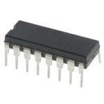
| 描述 | IC DAC 8BIT V-OUT 16-DIP数模转换器- DAC IC MONO 8-BIT |
| 产品分类 | |
| 品牌 | Analog Devices |
| 产品手册 | |
| 产品图片 |
|
| rohs | 符合RoHS无铅 / 符合限制有害物质指令(RoHS)规范要求 |
| 产品系列 | 数据转换器IC,数模转换器- DAC,Analog Devices AD558JNZDACPORT® |
| 数据手册 | |
| 产品型号 | AD558JNZ |
| 产品培训模块 | http://www.digikey.cn/PTM/IndividualPTM.page?site=cn&lang=zhs&ptm=19145http://www.digikey.cn/PTM/IndividualPTM.page?site=cn&lang=zhs&ptm=18614http://www.digikey.cn/PTM/IndividualPTM.page?site=cn&lang=zhs&ptm=26125http://www.digikey.cn/PTM/IndividualPTM.page?site=cn&lang=zhs&ptm=26140http://www.digikey.cn/PTM/IndividualPTM.page?site=cn&lang=zhs&ptm=26150http://www.digikey.cn/PTM/IndividualPTM.page?site=cn&lang=zhs&ptm=26147 |
| 产品目录页面 | |
| 产品种类 | 数模转换器- DAC |
| 位数 | 8 |
| 供应商器件封装 | 16-PDIP |
| 分辨率 | 8 bit |
| 包装 | 管件 |
| 商标 | Analog Devices |
| 安装类型 | 通孔 |
| 安装风格 | Through Hole |
| 封装 | Tube |
| 封装/外壳 | 16-DIP(0.300",7.62mm) |
| 封装/箱体 | PDIP-16 |
| 工作温度 | 0°C ~ 70°C |
| 工厂包装数量 | 25 |
| 建立时间 | 800ns |
| 接口类型 | Parallel |
| 数据接口 | 并联 |
| 最大功率耗散 | 450 mW |
| 最大工作温度 | + 70 C |
| 最小工作温度 | 0 C |
| 标准包装 | 25 |
| 电压参考 | Internal |
| 电压源 | 单电源 |
| 电源电压-最大 | 16.5 V |
| 电源电压-最小 | 4.5 V |
| 积分非线性 | +/- 0.5 LSB |
| 稳定时间 | 2 us |
| 系列 | AD558 |
| 结构 | R-2R |
| 转换器数 | 1 |
| 转换器数量 | 1 |
| 输出数和类型 | 1 电压,单极1 电压,双极 |
| 输出类型 | Voltage Unbuffered |
| 采样率(每秒) | - |


- 商务部:美国ITC正式对集成电路等产品启动337调查
- 曝三星4nm工艺存在良率问题 高通将骁龙8 Gen1或转产台积电
- 太阳诱电将投资9.5亿元在常州建新厂生产MLCC 预计2023年完工
- 英特尔发布欧洲新工厂建设计划 深化IDM 2.0 战略
- 台积电先进制程称霸业界 有大客户加持明年业绩稳了
- 达到5530亿美元!SIA预计今年全球半导体销售额将创下新高
- 英特尔拟将自动驾驶子公司Mobileye上市 估值或超500亿美元
- 三星加码芯片和SET,合并消费电子和移动部门,撤换高东真等 CEO
- 三星电子宣布重大人事变动 还合并消费电子和移动部门
- 海关总署:前11个月进口集成电路产品价值2.52万亿元 增长14.8%


PDF Datasheet 数据手册内容提取
REV. B Rev. B Document Feedback Information furnished by Analog Devices is believed to be accurate and reliable. However, no responsibility is assumed by Analog Devices for its use, nor for any infringements of patents or other One Technology Way, P.O. Box 9106, Norwood, MA 02062-9106, U.S.A. rights of third parties that may result from its use. Specifications subject to change without notice. No license is granted by implication or otherwise under any patent or patent rights of Analog Devices. Tel: 781.329.4700 ©1987–2017 Analog Devices, Inc. All rights reserved. Trademarks and registered trademarks are the property of their respective owners. Technical Support www.analog.com
AD558–SPECIFICATIONS (@ T = +25(cid:56)C, V = +5 V to +15 V unless otherwise noted) A CC Model AD558J AD558K AD558S1 AD558T1 Min Typ Max Min Typ Max Min Typ Max Min Typ Max Units RESOLUTION 8 8 8 8 Bits RELATIVE ACCURACY2 0(cid:176)C to +70(cid:176)C – 1/2 – 1/4 – 1/2 – 1/4 LSB –55(cid:176)C to +125(cid:176)C – 3/4 – 3/8 LSB OUTPUT Ranges3 0 to +2.56 0 to +2.56 0 to +2.56 0 to +2.56 V 0 to +10 0 to +10 0 to +10 0 to +10 V Current Source +5 +5 +5 +5 mA Sink Internal Passive Internal Passive Internal Passive Internal Passive Pull-Down to Ground4 Pull-Down to Ground Pull-Down to Ground Pull-Down to Ground OUTPUT SETTLING TIME5 0 to 2.56 Volt Range 0.8 1.5 0.8 1.5 0.8 1.5 0.8 1.5 m s 0 to 10 Volt Range4 2.0 3.0 2.0 3.0 2.0 3.0 2.0 3.0 m s FULL-SCALE ACCURACY6 @ 25(cid:176)C (cid:54)1.5 (cid:54)0.5 (cid:54)1.5 (cid:54)0.5 LSB T to T (cid:54)2.5 (cid:54)1 (cid:54)2.5 (cid:54)1 LSB MIN MAX ZERO ERROR @ 25(cid:176)C (cid:54)1 (cid:54)1/2 (cid:54)1 (cid:54)1/2 LSB T to T (cid:54)2 (cid:54)1 (cid:54)2 (cid:54)1 LSB MIN MAX MONOTONICITY7 T to T Guaranteed Guaranteed Guaranteed Guaranteed MIN MAX DIGITAL INPUTS T to T MIN MAX Input Current – 100 – 100 – 100 100 m A Data Inputs, Voltage Bit On-Logic “1” 2.0 2.0 2.0 2.0 V Bit On-Logic “0” 0 0.8 0 0 0 V Control Inputs, Voltage On-Logic “1” 2.0 2.0 2.0 2.0 V On-Logic “0” 0 0.8 0 0.8 0 0.8 0 0.8 V Input Capacitance 4 4 4 4 pF TIMING8 t , Strobe Pulse Width 200 200 200 200 ns W T to T 270 270 270 270 ns MIN MAX t Data Hold Time 10 10 10 10 ns DH T to T 10 10 10 10 ns MIN MAX t Data Set-Up Time 200 200 200 200 ns DS T to T 270 270 270 270 ns MIN MAX POWER SUPPLY Operating Voltage Range (V ) CC 2.56 Volt Range +4.5 +16.5 +4.5 +16.5 +4.5 +16.5 +4.5 +16.5 V 10 Volt Range +11.4 +16.5 +11.4 +16.5 +11.4 +16.5 +11.4 +16.5 V Current (I ) 15 25 15 25 15 25 15 25 mA CC Rejection Ratio 0.03 0.03 0.03 0.03 %/% POWER DISSIPATION, V = 5 V 75 125 75 125 75 125 75 125 mW CC V = 15 V 225 375 225 375 225 375 225 375 mW CC OPERATING TEMPERATURE RANGE 0 +70 0 +70 –55 +125 –55 +125 (cid:176)C NOTES 1The AD558 S & T grades are available processed and screened lo MIL-STD-883 Class B. Consult Analog Devices’ Military Databook for details. 2Relative Accuracy is defined as the deviation of the code transition points from the ideal transfer point on a straight line from the offset to the full scale of the device. See “Measuring Offset Error”. 3Operation of the 0 volt to 10 volt output range requires a minimum supply voltage of +11.4 volts. 4Passive pull-down resistance is 2 kW for 2.56 volt range, 10 kW for 10 volt range. 5Settling time is specified for a positive-going full-scale step to – 1/2 LSB. Negative-going steps to zero are slower, but can be improved with an external pull-down. 6The full range output voltage for the 2.56 range is 2.55 V and is guaranteed with a +5 V supply, for the 10 V range, it is 9.960 V guaranteed with a +15 V supply. 7A monotonic converter has a maximum differential linearity error of – 1 LSB. 8See Figure 7. Specifications shown in boldface are tested on all production units at final electrical test. Specifications subject to change without notice. –2– REV. B
AD558 ABSOLUTE MAXIMUM RATINGS* V to Ground . . . . . . . . . . . . . . . . . . . . . . . . . . . 0 V to +18 V (LSB) DB0 1 16 VOUT DCigCital Inputs (Pins 1–10) . . . . . . . . . . . . . . . . . .0 V to +7.0 V DB1 2 15 VOUT SENSE V . . . . . . . . . . . . . . . . . . . . . . . Indefinite Short to Ground DB2 3 14 VOUT SELECT OUT Momentary Short to V DB3 4 AD558 13 GND Power Dissipation . . . . . . . . . . . . . . . . . . . . . . . . . . . .450 mCWC DB4 5 (NToOt Pto V SIEcaWle) 12 GND Storage Temperature Range DB5 6 11 +VCC N/P (Plastic) Packages . . . . . . . . . . . . . . . .–25(cid:176) C to +100(cid:176) C DB6 7 10 CS D (Ceramic) Package . . . . . . . . . . . . . . . . .–55(cid:176) C to +150(cid:176) C (MSB) DB7 8 9 CE Lead Temperature (soldering, 10 sec) . . . . . . . . . . . . . +300(cid:176) C Figure 1a.AD558 Pin Configuration (DIP) Thermal Resistance Junction to Ambient/Junction to Case E D (Ceramic) Package . . . . . . . . . . . . . . 100(cid:176) C/W/30(cid:176) C/W B) NS S E N/P (Plastic) Packages . . . . . . . . . . . . . 140(cid:176) C/W/55(cid:176) C/W B1 B0 (L C OUTSOUT *Stresses greater than those listed under “Absolute Maximum Ratings” may cause D D NV V permanent damage to the device. This is a stress rating only and functional 3 2 1 20 19 operation of the device at these or any other conditions above those indicated in the operational section of this specification is not implied. Exposure to absolute maximum rating conditions for extended periods may affect device reliability. DB2 4 18 VOUT SELECT DB3 5 AD558 17 GND NC 6 TOP VIEW 16 NC AD558 METALIZATION PHOTOGRAPH DB4 7 (Not to Scale) 15 GND Dimensions shown in inches and (mm). DB5 8 14 +VCC 9 10 1112 13 6 7 C E S B B N C C D D B) NC = NO CONNECT S M ( Figure 1b.AD558 Pin Configuration (PLCC and LCC) Bond Pad Coordinates Pad No. Pad Name X Coordinate Y Coordinate 1 DB0 −702 1265 2 DB1 −927 1265 3 DB2 −957 1004 4 DB3 −957 347 5 DB4 −957 115 6 DB5 −957 −111 7 DB6 −927 −1248 8 DB7 −702 −1248 9 CE 47 −1248 10 CS 272 −1248 11 VCC 957 −1225 122 GND 957 −965 133 GND 946 970 14 VOUTSELECT 923 1265 15 VOUTSENSE 689 1265 16 VOUT −461 1265 REV. B –3–
AD558 CIRCUIT DESCRIPTION CHIP AVAILABILITY The AD558 consists of four major functional blocks, fabricated The AD558 is available in laser-trimmed, passivated chip form. on a single monolithic chip (see Figure 2). The main D-to-A AD558J and AD558T chips are available. Consult the factory converter section uses eight equally-weighted laser-trimmed for details. current sources switched into a silicon-chromium thin-film Input Logic Coding R/2R resistor ladder network to give a direct but unbuffered 0 mV to 400 mV output range. The transistors that form the Digital Input Code Output Voltage DAC switches are PNPs; this allows direct positive-voltage logic Binary Hexadecimal Decimal 2.56 V Range 10.000 V Range interface and a zero-based output range. 0000 0000 00 0 0 0 0000 0001 01 1 0.010 V 0.039 V DIGITAL INPUT DATA CONTROL 0000 0010 02 2 0.020 V 0.078 V INPUTS 0000 1111 0F 15 0.150 V 0.586 V LSB MSB CS CE DB0 DB1 DB2 DB3 DB4 DB5 DB6 DB7 +VCC GND GND 00010111 01010101 170F 11627 01..126700 VV 04..692651 VV 1000 0000 80 128 1.280 V 5.000 V I2L CONTROL I2L LATCHES 1100 0000 C0 192 1.920 V 7.500 V LOGIC 1111 1111 FF 255 2.55 V 9.961 V BAND- OUTPUT REFGERAEPNCE 8-BIT VOLTAGE-SWITCHING AMP CONNECTING THE AD558 D-TO-A CONVERTER VOUT The AD558 has been configured for ease of application. All ref- CONTROL AMP VOUTSENSE erence, output amplifier and logic connections are made inter- nally. In addition, all calibration trims are performed at the VOUTSELECT factory assuring specified accuracy without user trims. The only connection decision that must be made by the user is a single jumper to select output voltage range. Clean circuit board lay- Figure 2.AD558 Functional Block Diagram out is facilitated by isolating all digital bit inputs on one side of The high speed output buffer amplifier is operated in the non- the package; analog outputs are on the opposite side. inverting mode with gain determined by the user-connections Figure 3 shows the two alternative output range connections. at the output range select pin. The gain-setting application The 0 V to 2.56 V range may be selected for use with any power resistors are thin-film laser-trimmed to match and track the supply between +4.5 V and +16.5 V. The 0 V to 10 V range DAC resistors and to assure precise initial calibration of the two requires a power supply of +11.4 V to +16.5 V. output ranges, 0 V to 2.56 V and 0 V to 10 V. The amplifier output stage is an NPN transistor with passive pull-down for zero-based output capability with a single power supply. The OUTPUT OUTPUT AMP AMP internal precision voltage reference is of the patented bandgap type. This design produces a reference voltage of 1.2 volts and 16 VOUT 16 VOUT thus, unlike 6.3 volt temperature compensated Zeners, may be operated from a single, low voltage logic power supply. The 15 VOUT SENSE 15 VOUT SENSE microprocessor interface logic consists of an 8-bit data latch and 14 VOUT SELECT 14 VOUT SELECT control circuitry. Low power, small geometry and high speed are advantages of the I2L design as applied to this section. I2L is 13 GND 13 GND bipolar process compatible so that the performance of the ana- log sections need not be compromised to provide on-chip logic a.0 V to 2.56 V Output Range b.0 V to 10 V Output Range capabilities. The control logic allows the latches to be operated Figure 3.Connection Diagrams from a decoded microprocessor address and write signal. If the application does not involve a m P or data bus, wiring CS and Because of its precise factory calibration, the AD558 is intended to be operated without user trims for gain and offset; therefore CE to ground renders the latches “transparent” for direct DAC no provisions have been made for such user trims. If a small in- access. crease in scale is required, however, it may be accomplished by slightly altering the effective gain of the output buffer. A MIL-STD-883 resistor in series with V SENSE will increase the output The rigors of the military/aerospace environment, temperature OUT range. extremes, humidity, mechanical stress, etc., demand the utmost in electronic circuits. The AD558, with the inherent reliability For example if a 0 V to 10.24 V output range is desired (40 mV of integrated circuit construction, was designed with these ap- = 1 LSB), a nominal resistance of 850 W is required. It must be plications in mind. The hermetically-sealed, low profile DIP remembered that, although the internal resistors all ratio- package takes up a fraction of the space required by equivalent match and track, the absolute tolerance of these resistors is modular designs and protects the chip from hazardous environ- typically – 20% and the absolute TC is typically –50 ppm/(cid:176) C ments. To further ensure reliability, military temperature range (0 to –100 ppm/(cid:176) C). That must be considered when rescaling is AD558 grades S and T are available screened to MIL-STD-883. performed. Figure 4 shows the recommended circuitry for a For more complete data sheet information consult the Analog full-scale output range of 10.24 volts. Internal resistance values Devices’ Military Databook. shown are nominal. –4– REV. B
Applications–AD558 The only consideration in selecting a supply voltage is that, in OUTPUT order to be able to use the 0 V to 10 V output range, the power AMP supply voltage must be between +11.4 V and +16.5 V. If, how- 16 VOUT ever, the 0 V to 2.56 V range is to be used, power consumption 500W 604W will be minimized by utilizing the lowest available supply voltage 15 40kW (above +4.5 V). 14 2kW 14kW TIMING AND CONTROL 13 GND The AD558 has data input latches that simplify interface to 8- and 16-bit data buses. These latches are controlled by Chip Figure 4.10.24 V Full-Scale Connection Enable (CE) and Chip Select (CS) inputs. CE and CS are inter- nally “NORed” so that the latches transmit input data to the NOTE: Decreasing the scale by putting a resistor in series with GND DAC section when both CE and CS are at Logic “0”. If the ap- will not work properly due to the code-dependent currents in GND. plication does not involve a data bus, a “00” condition allows Adjusting offset by injecting dc at GND is not recommended for the for direct operation of the DAC. When either CE or CS go to same reason. Logic “1”, the input data is latched into the registers and held until both CE and CS return to “0”. (Unused CE or CS inputs GROUNDING AND BYPASSING* should be tied to ground.) The truth table is given in Table I. All precision converter products require careful application of The logic function is also shown in Figure 6. good grounding practices to maintain full rated performance. Because the AD558 is intended for application in microcom- Table I. AD558 Control Logic Truth Table puter systems where digital noise is prevalent, special care must be taken to assure that its inherent precision is realized. Latch The AD558 has two ground (common) pins; this minimizes Input Data CE CS DAC Data Condition ground drops and noise in the analog signal path. Figure 5 0 0 0 0 “Transparent” shows how the ground connections should be made. 1 0 0 1 “Transparent” 0 g 0 0 Latching OUTPUT 1 g 0 1 Latching AMP 0 0 g 0 Latching VOUT 16 1 0 g 1 Latching VOUT SENSE X 1 X Previous Data Latched 15 X X 1 Previous Data Latched 14VOUT SELECT (SEPEA GNEE)XT RL NOTES GND X = Does not matter. 13 g = Logic Threshold at Positive-Going Transition. TO SYSTEM GND 12 TO SYSTEM GND GND 0.1mF (SEE TEXT) 11 TO SYSTEM VCC +VCC Figure 5.Recommended Grounding and Bypassing It is often advisable to maintain separate analog and digital grounds throughout a complete system, tying them common in one place only. If the common tie-point is remote and acciden- tal disconnection of that one common tie-point occurs due to card removal with power on, a large differential voltage between the two commons could develop. To protect devices that inter- face to both digital and analog parts of the system, such as the Figure 6.AD558 Control Logic Function AD558, it is recommended that common ground tie-points In a level-triggered latch such as that in the AD558 there is an should be provided at each such device. If only one system interaction between data setup and hold times and the width of ground can be connected directly to the AD558, it is recom- the enable pulse. In an effort to reduce the time required to test mended that analog common be selected. all possible combinations in production, the AD558 is tested with t = t = 200 ns at 25(cid:176) C and 270 ns at T and T , DS W MIN MAX POWER SUPPLY CONSIDERATIONS with t = 10 ns at all temperatures. Failure to comply with DH The AD558 is designed to operate from a single positive power these specifications may result in data not being latched properly. supply voltage. Specified performance is achieved for any supply Figure 7 shows the timing for the data and control signals; CE voltage between +4.5 V and +16.5 V. This makes the AD558 and CS are identical in timing as well as in function. ideal for battery-operated, portable, automotive or digital main- frame applications. *For additional insight, “An IC Amplifier Users’ Guide to Decoupling, Grounding and Making Things Go Right For A change,” is available at no charge from any Analog Devices Sales Office. REV. B –5–
AD558 DATA tDH2.0V 16 VOUT INPUTS tDS AD558 0.8V 15 VOUTSENSE RL CS OR CE 2.0V 0.8V NEGATIVE RP-D = 2x VEE tW SUPPLY VEE (in kW) Figure 9.Improved Settling Time 1/2 LSB available, bipolar output ranges may be achieved by suitable DAC output offsetting and scaling. Figure 10 shows how a – 1.28 volt V OUTPUT output range may be achieved when a –5 volt power supply is tSETTLING available. The offset is provided by the AD589 precision 1.2 volt tW = STORAGE PULSE WIDTH = 200ns MIN reference which will operate from a +5 volt supply. The AD544 tDH = DATA HOLD TIME = 10ns MIN output amplifier can provide the necessary – 1.28 volt output tDS = DATA SETUP TIME = 200ns MIN swing from – 5 volt supplies. Coding is complementary offset tSETTLING = DAC OUTPUT SETTLING TIME TO –1/2 LSB binary. Figure 7.AD558 Timing 5kW V = 0V TO +2.56V USE OF V SENSE OUT +5V OUT 0.01mF Separate access to the feedback resistor of the output amplifier 16 allows additional application versatility. Figure 8a shows how 5kW I · R drops in long lines to remote loads may be cancelled by AD558 15 AD544 putting the drops “inside the loop.” Figure 8b shows how the 14 4.53kW 0.01mF VO separate sense may be used to provide a higher output current 12 13 1.5kW +1.28 TO 500W –1.27 by feeding back around a simple current booster. BIPOLAR VIN OFFSET –5V AD589 ADJUST AD558 1165 VVOOUUTTSENSE 0VV TOOU T+10V 0.01mF 4–.17.k2WV IN0P00U0T0 0C0O0DE V+1OU2T8V 10000000 0V 12 13 14 RL 11111111 –1.27V GND GAIN –5V SELECT Figure 10.Bipolar Operation of AD558 from – 5 V Supplies a. Compensation for I· R Drops in Output Lines MEASURING OFFSET ERROR VCC One of the most commonly specified endpoint errors associated with real-world nonideal DACs is offset error. VOUT AD558 16 2N2222 In most DAC testing, the offset error is measured by applying 15 VOUTSENSE VOUT the zero-scale code and measuring the output deviation from 0 0V TO +2.56V volts. There are some DACs, like the AD558 where offset errors 12 13 14 GND GSEALINECT RL may be present but not observable at the zero scale, because of other circuit limitations (such as zero coinciding with single- supply ground) so that a nonzero output at zero code cannot be read as the offset error. Factors like this make testing the b.Output Current Booster AD558 a little more complicated. Figure 8.Use of V Sense OUT By adding a pulldown resistor from the output to a negative OPTIMIZING SETTLING TIME supply as shown in Figure 11, we can now read offset errors In order to provide single-supply operation and zero-based at zero code that may not have been observable due to circuit output voltage ranges, the AD558 output stage has a passive limitations. The value of the resistor should be such that, at zero “pull-down” to ground. As a result, settling time for negative voltage out, current through the resistor is 0.5 mA max. going output steps may be longer than for positive-going output steps. The relative difference depends on load resistance and OUTPUT capacitance. If a negative power supply is available, the AMP negative-going settling time may be improved by adding a pull- 0.5mA down resistor from the output to the negative supply as shown 16 VOUT –V in Figure 9. The value of the resistor should be such that, at 15 VOUT SENSE zero voltage out, current through that resistor is 0.5 mA max. 14 VOUT SELECT BIPOLAR OUTPUT RANGES 13 AGND The AD558 was designed for operation from a single power supply and is thus capable of providing only unipolar (0 V to +2.56 V and 0 V to 10 V) output ranges. If a negative supply is a.0 V to 2.56 V Output Range –6– REV. B
AD558 OUTPUT ADDRESS BUS AMP 16 VOUT 0.5mA 16 16 –V ADDRESS SELECT 15 VOUT SENSE PULSE LOGIC 14 VOUT SELECT 8080A CS AD558 VOUT MEMW CE 13 AGND DB0–DB7 b.0 V to 10 V Output Range 8 Figure 11.Offset Connection Diagrams 8 DATA BUS INTERFACING THE AD558 TO MICROPROCESSOR MEMW fi CE DATA BUSES DECODED ADDRESS SELECT PULSE fi CS The AD558 is configured to act like a “write only” location in b.8080A/AD558 Interface memory that may be made to coincide with a read only memory location or with a RAM location. The latter case allows data 8 previously written into the DAC to be read back later via the ADDRESS BUS RAM. Address decoding is partially complete for either ROM or RAM. Figure 12 shows interfaces for three popular micropro- MA 0 – 7 8 cessor systems. TPA ADDRESS CS LATCH ADDRESS BUS 1802 DEC&ODE AD558 VOUT MWR CE 16 16 DB0–DB7 ADDRESS 6800 DECODER 8 8 VMA CS VOUT DATA BUS AD558 f2 CDP 1802: MWR fi CE DECODED ADDRESS SELECT PULSE fi CS CE R/W DB0–DB7 c.1802/AD558 Interface Figure 12.Interfacing the AD558 to Microprocessors 8 8 DATA BUS R/W fi CE GATED DECODED ADDRESS fi CS a.6800/AD558 Interface Performance (typical @ +25(cid:56)C, V (cid:54) +5 V to +15 V unless otherwise noted) CC LSB 1.75 1.50 1.25 ALL AD558 LSB ALL AD558 1.00 AD558S, T 1/2 AD558S, T 0.75 ZERO ERROR 0.50 1/4 0.25 FULL 0 0 SCALE ERROR –0.25 –55 –25 0 +25 +50 +75 +100 +125 oC –0.50 –1/4 –0.75 –1.00 –1/2 1LSB = 0.39% OF FULL SCALE –55 –25 0 +25 +50 +75 +100 +125 oC 1LSB = 0.39% OF FULL SCALE Figure 13.Full-Scale Accuracy vs. Temperature Figure 14.Zero Drift vs. Temperature Performance Performance of AD558 of AD558 REV. B –7–
OUTLINE DIMENSIONS AD558 0.775 0.755 mA 0.735 16 16 9 0.280 PIN 1 0.250 INDICATOR 1 8 0.240 14 ICC 0.100 TOP VIEW 0.325 BSC 0.195 0.310 12 0M.2A1X0 SIDE VIEW 00..111350 0.300 0.015 0.150 MIN 0.015 10 00..111350 SEATING GPALUAGNEE END VIEW 00..001120 0.022 0.021PLANE 0.430 0.008 0.018 0.070 0.016 MAX 0.015 0.0450.060 0.011 0.0390.055 4 6 8 10 12 14 16 18 VOLTS 0.030COMPLIANT TO JEDEC STANDARDS MS-001-BB 03-07-2014-D 16-Lead Plastic Dual In-Line Package [PDIP] VCC Narrow Body (N-16) Figure 15.Quiescent Current vs. Power Supply Dimensions shown in inches Voltage for AD558 0.005 (0.13) MIN 0.080 (2.03) MAX 16 9 0.310 (7.87) PIN 1 0.220 (5.59) 1 8 0.320 (8.13) 0.200 (5.08) 0.840 (21.34) MAX 0.060 (1.52) 0.290 (7.37) MAX 0.015 (0.38) 0.150 (3.81) 0.200 (5.08) MIN 0.125 (3.18) 0.100 0.070 (1.78)SEATING 0.015 (0.38) 0.023 (0.58) (B2.S5C4)0.030 (0.76)PLANE 0.008 (0.20) 0.014 (0.36) CONTROLLING DIMENSIONS ARE IN INCHES; MILLIMETER DIMENSIONS (IN PARENTHESES) ARE ROUNDED-OFF INCH EQUIVALENTS FOR REFERENCE ONLY AND ARE NOT APPROPRIATE FOR USE IN DESIGN. 16-Lead Side-Brazed Ceramic Dual In-Line Package [SBDIP] (D-16) Figure 16.AD558 Settling Characteristics Detail Dimensions shown in inches and (millimeters) 0 V to 2.56 V Output Range Full-Scale Step 0.180 (4.57) 0.048 (1.22 ) 0.165 (4.19) 0.042 (1.07) 0.056 (1.42) 0.042 (1.07) 0M.2IN0 (0.51) 0.020R (0.50) 3 19 00..004482 ((11..2027)) 4 IDEPNITNI F1IER 18 (01.0.2570) 00..002113 ((00..5333))0.330 (8.38) BOTTOM TOP VIEW BSC 0.032 (0.81)0.290 (7.37) VIEW (PINS DOWN) 0.026 (0.66) (PINS UP) 8 14 9 13 0.020 0.045 (1.14) (0.R51) 00..335560 ((98..0849))SQ 0.025 (0.64)R 0.120 (3.04) 0.395 (10.03)SQ 0.090 (2.29) 0.385 (9.78) COMPLIANT TO JEDEC STANDARDS MO-047-AA CONTROLLING DIMENSIONS ARE IN INCHES; MILLIMETER DIMENSIONS (IN PARENTHESES) ARE ROUNDED-OFF INCH EQUIVALENTS FOR REFERENCE ONLY AND ARE NOT APPROPRIATE FOR USE IN DESIGN. Figure 17.AD558 Settling Characteristic Detail 20-Lead Plastic Leaded Chip Carrier [PLCC] (P-20) 0 V to 10 V Output Range Full-Scale Step Dimensions shown in inches and (millimeters) A. 0.075 (1.91) 0R.E2F00 (5.08) U.S. 00..100604 ((21..5643)) 0.095 (2.4R1E)F 0.1000 .(021.554 ()0 R.3E8F) D IN 0.075 (1.90) 19 3 MIN NTE 0.358 (9.09) 0.358 18 20 1 4 0.028 (0.71) PRI 0.342 (8.69) (9.09) 0.011 (0.28) BOTTOM 0.022 (0.56) SQ MSAQX 0.007R (0 T.1Y8P) VIEW 0.050 (1.27) 0.075 (1.91) 14 8 BSC REF 13 9 45° TYP 0.088 (2.24) 0.055 (1.40) 0.150 (3.81) 0.054 (1.37) 0.045 (1.14) BSC C(RINOE FNPEATRRREOENNLCLTEIHN EOGSN DELISYM)A EANNRDSEI AORRNOESU NANORDETE DAIN-PO IPNFRFCO HINPECRSHI;A MTEEQIL UFLOIIVMRAE LUTEESNRET DISNI M FDOEERNSSIGIONN.S 022106-A 20-Terminal Ceramic Leadless Chip Carrier [LCC] Figure 18.AD558 Logic Timing (E-20-1) Dimensions shown in inches and (millimeters) –8– REV. B
Data Sheet AD558 ORDERING GUIDE Relative Accuracy Error Max Full Scale Error Max Model Temperature Range T to T T to T Package Option MIN MAX MIN MAX AD558JN 0°C to +70°C ±1/2 LSB ±2.5 LSB PDIP (N-16) AD558JNZ 0°C to +70°C ±1/2 LSB ±2.5 LSB PDIP (N-16) AD558JP 0°C to +70°C ±1/2 LSB ±2.5 LSB PLCC (P-20) AD558JP-REEL7 0°C to +70°C ±1/2 LSB ±2.5 LSB PLCC (P-20) AD558JPZ 0°C to +70°C ±1/2 LSB ±2.5 LSB PLCC (P-20) AD558JPZ-REEL 0°C to +70°C ±1/2 LSB ±2.5 LSB PLCC (P-20) AD558JPZ-REEL7 0°C to +70°C ±1/2 LSB ±2.5 LSB PLCC (P-20) AD558JD 0°C to +70°C ±1/2 LSB ±2.5 LSB SBDIP (D-16) AD558KN 0°C to +70°C ±1/4 LSB ±1 LSB PDIP (N-16) AD558KNZ 0°C to +70°C ±1/4 LSB ±1 LSB PDIP (N-16) AD558KP 0°C to +70°C ±1/4 LSB ±1 LSB PLCC (P-20) AD558KPZ 0°C to +70°C ±1/4 LSB ±1 LSB PLCC (P-20) AD558KPZ-REEL7 0°C to +70°C ±1/4 LSB ±1 LSB PLCC (P-20) AD558KD 0°C to +70°C ±1/4 LSB ±1 LSB SBDIP (D-16) AD558SD –55°C to +125°C ±3/4 LSB ±2.5 LSB SBDIP (D-16) AD558TD –55°C to +125°C ±3/8 LSB ±1 LSB SBDIP (D-16) AD558TCHIPS –55°C to +125°C ±3/8 LSB ±1 LSB Die part AD558SD/883B –55°C to +125°C ±3/4 LSB ±2.5 LSB SBDIP (D-16) AD558SE/883B –55°C to +125°C ±3/4 LSB ±2.5 LSB LCC (E-20-1) AD558TD/883B –55°C to +125°C ±3/8 LSB ±1 LSB SBDIP (D-16) AD558TE/883B –55°C to +125°C ±3/8 LSB ±1 LSB LCC (E-20-1) 1 For details on grade and package offerings screened in accordance with MIL-STD-883, refer to the Analog Devices Military Products Databook or current AD558/883B data sheet. 2S = Ceramic SBDIP; N = Plastic PDIP; P = Plastic Leaded Chip Carrier. REVISION HISTORY 6/2017—Rev. A to Rev. B Added Bond Pad Coordinates Table ............................................... 3 Updated Outline Dimensions .......................................................... 8 Changes to Ordering Guide ............................................................. 9 ©1987–2017 Analog Devices, Inc. All rights reserved. Trademarks and registered trademarks are the property of their respective owners. D09374-0-6/17(B) –9–
Mouser Electronics Authorized Distributor Click to View Pricing, Inventory, Delivery & Lifecycle Information: A nalog Devices Inc.: 5962-8778902EA AD558KPZ-REEL7 AD558JD AD558JPZ AD558TD/883B AD558KN 5962-87789012A AD558KP 5962-8778901EA AD558TE/883B AD558SE/883B AD558JP AD558JPZ-REEL7 AD558KD AD558SD AD558JN AD558JP-REEL7 AD558TD AD558KNZ 5962-87789022A AD558SD/883B AD558KPZ AD558JNZ