ICGOO在线商城 > 集成电路(IC) > 数据采集 - 数模转换器 > TLV5604IPW
 Datasheet下载
- 型号: TLV5604IPW
- 制造商: Texas Instruments
- 库位|库存: xxxx|xxxx
- 要求:
| 数量阶梯 | 香港交货 | 国内含税 |
| +xxxx | $xxxx | ¥xxxx |
查看当月历史价格
查看今年历史价格
TLV5604IPW产品简介:
ICGOO电子元器件商城为您提供TLV5604IPW由Texas Instruments设计生产,在icgoo商城现货销售,并且可以通过原厂、代理商等渠道进行代购。 TLV5604IPW价格参考¥43.53-¥80.47。Texas InstrumentsTLV5604IPW封装/规格:数据采集 - 数模转换器, 10 位 数模转换器 4 16-TSSOP。您可以下载TLV5604IPW参考资料、Datasheet数据手册功能说明书,资料中有TLV5604IPW 详细功能的应用电路图电压和使用方法及教程。
Texas Instruments(德州仪器)的TLV5604IPW是一款12位电压输出数模转换器(DAC),具有低功耗和小型封装的特点,适用于多种数据采集系统中的应用场景。以下是该型号的主要应用场景:

 1. 工业自动化与控制
TLV5604IPW常用于工业自动化系统中,特别是在需要精确控制模拟信号输出的地方。例如,在PLC(可编程逻辑控制器)或DCS(分布式控制系统)中,它可以通过数字输入生成精确的模拟电压输出,用于控制电机、阀门或其他执行器。其低功耗特性使其适合长时间运行的工业环境。

 2. 医疗设备
在医疗设备中,如心电图机、血压计等,TLV5604IPW可以用于将数字信号转换为模拟信号,驱动显示屏或传感器。由于其高精度和低噪声特性,能够确保医疗设备的测量结果更加准确可靠。此外,其小尺寸封装也使得它可以在紧凑型医疗设备中使用。

 3. 通信设备
在通信系统中,特别是无线基站或卫星通信设备中,TLV5604IPW可用于调整发射功率或接收信号的增益。通过精确的电压输出控制,它可以优化信号传输的质量,减少干扰并提高系统的稳定性。

 4. 音频处理
在音频设备中,如专业音频处理器或音响系统,TLV5604IPW可以用于将数字音频信号转换为模拟信号,驱动扬声器或耳机。其12位分辨率和低失真特性能够提供高质量的音频输出,特别适合对音质要求较高的应用。

 5. 测试与测量仪器
在测试与测量设备中,如示波器、信号发生器等,TLV5604IPW可以作为信号源的一部分,生成精确的模拟电压波形。其高精度和快速响应时间使其能够在这些设备中提供可靠的性能,帮助工程师进行更准确的测量和分析。

 6. 消费电子产品
在一些消费电子产品中,如智能家电或便携式设备,TLV5604IPW可以用于控制显示屏亮度、调节音量或驱动传感器。其低功耗和小尺寸封装使得它非常适合电池供电的便携式设备,延长了设备的续航时间。

总之,TLV5604IPW凭借其高精度、低功耗和小尺寸封装等特点,广泛应用于工业、医疗、通信、音频处理、测试测量以及消费电子等多个领域,满足了不同场景下对数模转换的需求。
| 参数 | 数值 |
| 产品目录 | 集成电路 (IC)半导体 |
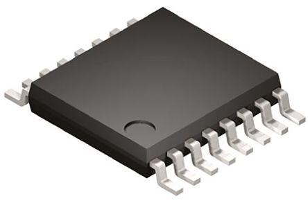
| 描述 | IC 10-BIT QUAD SER DAC 16-TSSOP数模转换器- DAC 10bit Quad Serial D |
| 产品分类 | |
| 品牌 | Texas Instruments |
| 产品手册 | |
| 产品图片 |
|
| rohs | 符合RoHS无铅 / 符合限制有害物质指令(RoHS)规范要求 |
| 产品系列 | 数据转换器IC,数模转换器- DAC,Texas Instruments TLV5604IPW- |
| 数据手册 | |
| 产品型号 | TLV5604IPW |
| 产品培训模块 | http://www.digikey.cn/PTM/IndividualPTM.page?site=cn&lang=zhs&ptm=13240 |
| 产品目录页面 | |
| 产品种类 | 数模转换器- DAC |
| 位数 | 10 |
| 供应商器件封装 | 16-TSSOP |
| 其它名称 | 296-1917 |
| 分辨率 | 10 bit |
| 制造商产品页 | http://www.ti.com/general/docs/suppproductinfo.tsp?distId=10&orderablePartNumber=TLV5604IPW |
| 包装 | 管件 |
| 单位重量 | 63 mg |
| 商标 | Texas Instruments |
| 安装类型 | 表面贴装 |
| 安装风格 | SMD/SMT |
| 封装 | Tube |
| 封装/外壳 | 16-TSSOP(0.173",4.40mm 宽) |
| 封装/箱体 | TSSOP-16 |
| 工作温度 | -40°C ~ 85°C |
| 工厂包装数量 | 90 |
| 建立时间 | 8.5µs |
| 接口类型 | QSPI, SPI, Serial (3-Wire, 4-Wire, Microwire) |
| 数据接口 | 串行 |
| 最大工作温度 | + 85 C |
| 最小工作温度 | - 40 C |
| 标准包装 | 90 |
| 电压参考 | External |
| 电压源 | 模拟和数字 |
| 电源电压-最大 | 5.5 V |
| 电源电压-最小 | 2.7 V |
| 积分非线性 | +/- 1 LSB |
| 稳定时间 | 18 us |
| 系列 | TLV5604 |
| 结构 | Resistor-String |
| 转换器数 | 4 |
| 转换器数量 | 1 |
| 输出数和类型 | 4 电压,单极 |
| 输出类型 | Voltage |
| 配用 | /product-detail/zh/TLV5604-08-31EVM/296-10733-ND/381824 |
| 采样比 | 102 kSPs |
| 采样率(每秒) | 102k |


- 商务部:美国ITC正式对集成电路等产品启动337调查
- 曝三星4nm工艺存在良率问题 高通将骁龙8 Gen1或转产台积电
- 太阳诱电将投资9.5亿元在常州建新厂生产MLCC 预计2023年完工
- 英特尔发布欧洲新工厂建设计划 深化IDM 2.0 战略
- 台积电先进制程称霸业界 有大客户加持明年业绩稳了
- 达到5530亿美元!SIA预计今年全球半导体销售额将创下新高
- 英特尔拟将自动驾驶子公司Mobileye上市 估值或超500亿美元
- 三星加码芯片和SET,合并消费电子和移动部门,撤换高东真等 CEO
- 三星电子宣布重大人事变动 还合并消费电子和移动部门
- 海关总署:前11个月进口集成电路产品价值2.52万亿元 增长14.8%


PDF Datasheet 数据手册内容提取
TLV5604 2.7-V TO 5.5-V 10-BIT 3-µS QUADRUPLE DIGITAL-TO-ANALOG CONVERTERS WITH POWER DOWN SLAS176B – DECEMBER 1997 – REVISED JULY 2002 (cid:0) (cid:0) Four 10-Bit D/A Converters Hardware Power Down (10 nA) (cid:0) (cid:0) Programmable Settling Time Software Power Down (10 nA) of 3 µs or 9 µs Typ (cid:0) Simultaneous Update (cid:0) TMS320, (Q)SPI, and Microwire Compatible Serial Interface applications (cid:0) Internal Power-On Reset (cid:0) Battery Powered Test Instruments (cid:0) Low Power Consumption: (cid:0) Digital Offset and Gain Adjustment 5.5 mW, Slow Mode – 5-V Supply (cid:0) Industrial Process Controls 3.3 mW, Slow Mode – 3-V Supply (cid:0) (cid:0) Machine and Motion Control Devices Reference Input Buffers (cid:0) (cid:0) Communications Voltage Output Range...2× the Reference (cid:0) Arbitrary Waveform Generation Input Voltage (cid:0) Monotonic Over Temperature D OR PW PACKAGE (cid:0) Dual 2.7-V to 5.5-V Supply (Separate Digital (TOP VIEW) and Analog Supplies) DVDD 1 16 AVDD description PD 2 15 REFINAB LDAC 3 14 OUTA The TLV5604 is a quadruple 10-bit voltage output DIN 4 13 OUTB digital-to-analog converter (DAC) with a flexible SCLK 5 12 OUTC 4-wire serial interface. The 4-wire serial interface CS 6 11 OUTD allows glueless interface to TMS320, SPI, QSPI, FS 7 10 REFINCD and Microwire serial ports. The TLV5604 is DGND 8 9 AGND programmed with a 16-bit serial word comprised of a DAC address, individual DAC control bits, and a 10-bit DAC value. The device has provision for two supplies: one digital supply for the serial interface (via pins DV and DGND), DD and one for the DACs, reference buffers and output buffers (via pins AV and AGND). Each supply is DD independent of the other, and can be any value between 2.7 V and 5.5 V. The dual supplies allow a typical application where the DAC will be controlled via a microprocessor operating on a 3-V supply (also used on pins DV and DGND), with the DACs operating on a 5-V supply. Of course, the digital and analog supplies can be DD tied together. The resistor string output voltage is buffered by a x2 gain rail-to-rail output buffer. The buffer features a ClassAB output stage to improve stability and reduce settling time. A rail-to-rail output stage and a power-down mode makes it ideal for single voltage, battery based applications. The settling time of the DAC is programmable to allow the designer to optimize speed versus power dissipation. The settling time is chosen by the control bits within the 16-bit serial input string. A high-impedance buffer is integrated on the REFINAB and REFINCD terminals to reduce the need for a low source impedance drive to the terminal. REFINAB and REFINCD allow DACs A and B to have a different reference voltage then DACs C and D. The device, implemented with a CMOS process, is available in 16-terminal SOIC and TSSOP packages. The TLV5604C is characterized for operation from 0°C to 70°C. The TLV5604I is characterized for operation from –40°C to 85°C. Please be aware that an important notice concerning availability, standard warranty, and use in critical applications of TexasInstruments semiconductor products and disclaimers thereto appears at the end of this data sheet. SPI and QSPI are trademarks of Motorola, Inc. Microwire is a trademark of National Semiconductor Corporation. PRODUCTION DATA information is current as of publication date. Copyright 2002, Texas Instruments Incorporated Products conform to specifications per the terms of Texas Instruments standard warranty. Production processing does not necessarily include testing of all parameters. POST OFFICE BOX 655303 • DALLAS, TEXAS 75265 1
TLV5604 2.7-V TO 5.5-V 10-BIT 3-µS QUADRUPLE DIGITAL-TO-ANALOG CONVERTERS WITH POWER DOWN SLAS176B – DECEMBER 1997 – REVISED JULY 2002 AVAILABLE OPTIONS PACKAGE TA SOIC TSSOP (D) (PW) 0°C to 70°C TLV5604CD TLV5604CPW –40°C to 85°C TLV5604ID TLV5604IPW functional block diagram AVDD DVDD 15 16 1 REFINAB DAC A + _ Power-On 14 x2 OUTA Reset 10 10-Bit 10 DAC 14 Latch Serial 14-Bit 4 DIN Input Data Register and Control 2 2-Bit 2 Register Control 2 Data Power Down/ 7 Latch Speed Control FS DAC 5 Select/ SCLK Control 6 Logic CS 13 DAC B OUTB 12 DAC C OUTC REFINCD 11 DAC D OUTD 3 2 9 8 AGND DGND LDAC PD 2 POST OFFICE BOX 655303 • DALLAS, TEXAS 75265
TLV5604 2.7-V TO 5.5-V 10-BIT 3-µS QUADRUPLE DIGITAL-TO-ANALOG CONVERTERS WITH POWER DOWN SLAS176B – DECEMBER 1997 – REVISED JULY 2002 Terminal Functions TERMINAL II//OO DDEESSCCRRIIPPTTIIOONN NAME NO. AGND 9 Analog ground AVDD 16 Analog supply CS 6 I Chip select. This terminal is active low. DGND 8 Digital ground DIN 4 I Serial data input DVDD 1 Digital supply FS 7 I Frame sync input. The falling edge of the frame sync pulse indicates the start of a serial data frame shifted out to the TLV5604. PD 2 I Power-down pin. Powers down all DACs (overriding their individual power down settings), and all output stages. This terminal is active low. LDAC 3 I Load DAC. When the LDAC signal is high, no DAC output updates occur when the input digital data is read into the serial interface. The DAC outputs are only updated when LDAC is low. REFINAB 15 I Voltage reference input for DACs A and B. REFINCD 10 I Voltage reference input for DACs C and D. SCLK 5 I Serial Clock input OUTA 14 O DAC A output OUTB 13 O DAC B output OUTC 12 O DAC C output OUTD 11 O DAC D output absolute maximum ratings over operating free-air temperature range (unless otherwise noted)† Supply voltage, (DV , AV to GND) . . . . . . . . . . . . . . . . . . . . . . . . . . . . . . . . . . . . . . . . . . . . . . . . . . . . . . . . 7 V DD DD Supply voltage difference, (AV to DV ) . . . . . . . . . . . . . . . . . . . . . . . . . . . . . . . . . . . . . . . . . . –2.8 V to 2.8 V DD DD Digital input voltage range . . . . . . . . . . . . . . . . . . . . . . . . . . . . . . . . . . . . . . . . . . . . . . . . . –0.3 V to DV + 0.3 V DD Reference input voltage range . . . . . . . . . . . . . . . . . . . . . . . . . . . . . . . . . . . . . . . . . . . . . . –0.3 V to AV + 0.3 V DD Operating free-air temperature range, T : TLV5604C . . . . . . . . . . . . . . . . . . . . . . . . . . . . . . . . . . . 0°C to 70°C A TLV5604I . . . . . . . . . . . . . . . . . . . . . . . . . . . . . . . . . . –40°C to 85°C Storage temperature range, T . . . . . . . . . . . . . . . . . . . . . . . . . . . . . . . . . . . . . . . . . . . . . . . . . . . –65°C to 150°C stg Lead temperature 1,6 mm (1/16 inch) from case for 10 seconds . . . . . . . . . . . . . . . . . . . . . . . . . . . . . . . 260°C †Stresses beyond those listed under “absolute maximum ratings” may cause permanent damage to the device. These are stress ratings only, and functional operation of the device at these or any other conditions beyond those indicated under “recommended operating conditions” is not implied. Exposure to absolute-maximum-rated conditions for extended periods may affect device reliability. POST OFFICE BOX 655303 • DALLAS, TEXAS 75265 3
TLV5604 2.7-V TO 5.5-V 10-BIT 3-µS QUADRUPLE DIGITAL-TO-ANALOG CONVERTERS WITH POWER DOWN SLAS176B – DECEMBER 1997 – REVISED JULY 2002 recommended operating conditions MIN NOM MAX UNIT 5-V supply 4.5 5 5.5 SSuuppppllyy vvoollttaaggee, AAVVDDDD, DDVVDDDD VV 3-V supply 2.7 3 3.3 DVDD = 2.7 V 2 HHiigghh-lleevveell ddiiggiittaall iinnppuutt vvoollttaaggee, VVIIHH VV DVDD = 5.5 V 2.4 DVDD = 2.7 V 0.6 LLooww-lleevveell ddiiggiittaall iinnppuutt vvoollttaaggee, VVIILL VV DVDD = 5.5 V 1 5-V supply (see Note 1) 0 2.048 AVDD–1.5 RReeffeerreennccee vvoollttaaggee, VVreff ttoo RREEFFIINNAABB, RREEFFIINNCCDD tteerrmmiinnaall VV 3-V supply (see Note 1) 0 1.024 AVDD–1.5 Load resistance, RL 2 10 kΩ Load capacitance, CL 100 pF Serial clock rate, SCLK 20 MHz TLV5604C 0 70 OOppeerraattiinngg ffrreeee-aaiirr tteemmppeerraattuurree °°CC TLV5604I –40 85 NOTE 1: Voltages greater than AVDD/2 will cause output saturation for large DAC codes. electrical characteristics over recommended operating free-air temperature range (unless otherwise noted) static DAC specifications PARAMETER TEST CONDITIONS MIN TYP MAX UNIT Resolution 10 bits Integral nonlinearity (INL), end point adjusted See Note 2 ±1 LSB Differential nonlinearity (DNL) See Note 3 ±0.1 ±1 LSB EZS Zero scale error (offset error at zero scale) See Note 4 ±12 mV Zero scale error temperature coefficient See Note 5 10 ppm/°C EG Gain error See Note 6 ±0.6 %vooltfa FgSe Gain error temperature coefficient See Note 7 10 ppm/°C Zero scale gain –80 PPSSRRRR PPoowweerr ssuuppppllyy rreejjeeccttiioonn rraattiioo SSeeee NNootteess 88 aanndd 99 ddBB Gain –80 NOTES: 2. The relative accuracy or integral nonlinearity (INL) sometimes referred to as linearity error, is the maximum deviation of the output from the line between zero and full scale excluding the effects of zero code and full-scale errors. 3. The differential nonlinearity (DNL) sometimes referred to as differential error, is the difference between the measured and ideal 1 LSB amplitude change of any two adjacent codes. Monotonic means the output voltage changes in the same direction (or remains constant) as a change in the digital input code. 4. Zero-scale error is the deviation from zero voltage output when the digital input code is zero. 5. Zero-scale-error temperature coefficient is given by: EZS TC = [EZS (Tmax) – EZS (Tmin)]/Vref × 106/(Tmax – Tmin). 6. Gain error is the deviation from the ideal output (2Vref – 1 LSB) with an output load of 10 kΩ excluding the effects of the zero-error. 7. Gain temperature coefficient is given by: EG TC = [EG(Tmax) – EG (Tmin)]/Vref × 106/(Tmax – Tmin). 8. Zero-scale-error rejection ratio (EZS–RR) is measured by varying the AVDD from 5 ±0.5 V and 3 ±0.3 V dc, and measuring the proportion of this signal imposed on the zero-code output voltage. 9. Gain-error rejection ratio (EG-RR) is measured by varying the AVDD from 5 ±0.5 V and 3 ±0.3 V dc and measuring the proportion of this signal imposed on the full-scale output voltage after subtracting the zero scale change. 4 POST OFFICE BOX 655303 • DALLAS, TEXAS 75265
TLV5604 2.7-V TO 5.5-V 10-BIT 3-µS QUADRUPLE DIGITAL-TO-ANALOG CONVERTERS WITH POWER DOWN SLAS176B – DECEMBER 1997 – REVISED JULY 2002 electrical characteristics over recommended operating free-air temperature range (unless otherwise noted) (continued) individual DAC output specifications PARAMETER TEST CONDITIONS MIN TYP MAX UNIT VO Voltage output RL = 10 kΩ 0 AVDD–0.4 V % of FS Output load regulation accuracy RL = 2 kΩ vs 10 kΩ 0.1 0.25 voltage reference input (REFINAB, REFINCD) PARAMETER TEST CONDITIONS MIN TYP MAX UNIT VI Input voltage range See Note 10 0 AVDD–1.5 V RI Input resistance 10 MΩ CI Input capacitance 5 pF REFIN = 1 Vpp at 1 kHz + 1.024 V dc Reference feed through –75 dB (see Note 11) Slow 0.5 RReeffeerreennccee iinnppuutt bbaannddwwiiddtthh RREEFFIINN == 00.22 VVpp ++ 11.002244 VV ddcc MMHHzz Fast 1 NOTES: 10. Reference input voltages greater than VDD/2 will cause output saturation for large DAC codes. 11. Reference feedthrough is measured at the DAC output with an input code = 000 hex and a Vref(REFINAB or REFINCD) input = 1.024 Vdc + 1 Vpp at 1 kHz. digital inputs (D0–D11, CS, WEB, LDAC, PD) PARAMETER TEST CONDITIONS MIN TYP MAX UNIT IIH High-level digital input current VI = DVDD ±1 µA IIL Low-level digital input current VI = 0 V ±1 µA CI Input capacitance 3 pF power supply PARAMETER TEST CONDITIONS MIN TYP MAX UNIT Slow 1.4 2.2 55-VV ssuuppppllyy, NNoo llooaadd, CClloocckk rruunnnniinngg mmAA Fast 3.5 5.5 IIDDDD PPoowweerr ssuuppppllyy ccuurrrreenntt Slow 1 1.5 33-VV ssuuppppllyy, NNoo llooaadd, CClloocckk rruunnnniinngg mmAA Fast 3 4.5 Power down supply current, 10 nA See Figure 12 POST OFFICE BOX 655303 • DALLAS, TEXAS 75265 5
TLV5604 2.7-V TO 5.5-V 10-BIT 3-µS QUADRUPLE DIGITAL-TO-ANALOG CONVERTERS WITH POWER DOWN SLAS176B – DECEMBER 1997 – REVISED JULY 2002 electrical characteristics over recommended operating free-air temperature range (unless otherwise noted) (continued) analog output dynamic performance PARAMETER TEST CONDITIONS MIN TYP MAX UNIT CL = 100 pF, RL = 10 kΩ, Fast 5 V/µs SSRR OOuuttppuutt sslleeww rraattee VVOO = 1100%% ttoo 9900%%, Vref = 2.048 V, 1024 V Slow 1 V/µs tts OOuuttppuutt sseettttlliinngg ttiimmee TRoL ±=0 1.50 LkΩSB, ,, S CeLLe =N o1t0e0s p1F2,, and 14 SFlaoswt 28..55 148 µµss tts((c)) OOuuttppuutt sseettttlliinngg ttiimmee, ccooddee ttoo ccooddee TRoL ±=0 1.50 LkΩSB, ,, S eCeLL N=o 1te0 01 3pF,, SFlaoswt 12 µµss Glitch energy Code transition from 7FF to 800 10 nV-sec SNR Signal-to-noise ratio Sinewave generated by DAC, 68 RRefference volltage = 11.002244 at 33 VV andd 22.004488 at 55 VV, S/(N+D) Signal to noise + distortion 65 ffss == 440000 KKSSPPSS,, ddBB THD Total harmonic Distortion fOUT = 1.1 kHz sinewave, –68 CCLL == 110000 ppFF, RRLL == 1100 kkΩΩ, SFDR Spurious free dynamic range BW = 20 kHz 70 NOTES: 12. Settling time is the time for the output signal to remain within ±0.5LSB of the final measured value for a digital input code change of 020 hex to 3FF hex or 3FF hex to 020 hex. 13. Settling time is the time for the output signal to remain within ±0.5LSB of the final measured value for a digital input code change of one count, 1FF hex to 200 hex. 14. Limits are ensured by design and characterization, but are not production tested. 6 POST OFFICE BOX 655303 • DALLAS, TEXAS 75265
TLV5604 2.7-V TO 5.5-V 10-BIT 3-µS QUADRUPLE DIGITAL-TO-ANALOG CONVERTERS WITH POWER DOWN SLAS176B – DECEMBER 1997 – REVISED JULY 2002 electrical characteristics over recommended operating free-air temperature range (unless otherwise noted) (continued) digital input timing requirements MIN NOM MAX UNIT tsu(CS–FS) Setup time, CS low before FS↓ 10 ns tsu(FS–CK) Setup time, FS low before first negative SCLK edge 8 ns Setup time, sixteenth negative SCLK edge after FS low on which bit D0 is sampled before tsu(C16–FS) rising edge of FS 10 ns Setup time. The first positive SCLK edge after D0 is sampled before CS rising edge. If FS tsu(C16–CS) is used instead of the SCLK positive edge to update the DAC, then the setup time is between 10 ns the FS rising edge and CS rising edge. twH Pulse duration, SCLK high 25 ns twL Pulse duration, SCLK low 25 ns tsu(D) Setup time, data ready before SCLK falling edge 8 ns th(D) Hold time, data held valid after SCLK falling edge 5 ns twH(FS) Pulse duration, FS high 20 ns PARAMETER MEASUREMENT INFORMATION twL twH ÎÎÎÎ ÎÎ ÎÎÎÎ ÎÎ SCLK 1 2 3 4 5 15 16 ÎÎÎÎ ÎÎ tsu(D) th(D) ÎÎÎÎ ÎÎÎ DIN D15 D14 D13 D12 D1 D0 ÎÎÎÎ ÎÎÎ tsu(FS-CK) tsu(C16-CS) tsu(CS-FS) CS twH(FS) tsu(C16-FS) FS Figure 1. Timing Diagram POST OFFICE BOX 655303 • DALLAS, TEXAS 75265 7
TLV5604 2.7-V TO 5.5-V 10-BIT 3-µS QUADRUPLE DIGITAL-TO-ANALOG CONVERTERS WITH POWER DOWN SLAS176B – DECEMBER 1997 – REVISED JULY 2002 TYPICAL CHARACTERISTICS LOAD REGULATION LOAD REGULATION 0.35 0.20 VDD = 5 V, VDD = 3 V, VREF = 2 V, 0.18 VREF = 1 V, 0.30 VO = Full Scale VO = Full Scale 0.16 e – V 0.25 5 V Slow Mode, Sink e – V 0.14 3 V Slow Mode, Sink ag ag 0.12 olt 0.20 olt V V put 0.15 5 V Fast Mode, Sink put 0.10 3 V Fast Mode, Sink ut ut 0.08 O O – – O 0.10 O 0.06 V V 0.04 0.05 0.02 0 0 0 0.02 0.04 0.1 0.2 0.4 0.8 1 2 4 0 0.01 0.02 0.05 0.1 0.2 0.5 0.8 1 2 Load Current – mA Load Current – mA Figure 2 Figure 3 LOAD REGULATION LOAD REGULATION 4.002 2.003 4.00 2.0025 5 V Slow Mode, Source 3.998 3 V Fast Mode, Source 2.002 V V – 3.996 – ge ge 2.0015 a a Volt 3.994 5 V Fast Mode, Source Volt 3 V Slow Mode, Source put 3.992 put 2.001 ut ut O O 2.0005 – 3.99 – O O V V 2 3.988 VDD = 5 V, VDD = 3 V, 3.986 VREF = 2 V, 1.9995 VREF = 1 V, VO = Full Scale VO = Full Scale 3.984 1.999 0 0.02 0.04 0.1 0.2 0.4 0.8 1 2 4 0 0.01 0.02 0.05 0.1 0.2 0.5 0.8 1 2 Load Current – mA Load Current – mA Figure 4 Figure 5 8 POST OFFICE BOX 655303 • DALLAS, TEXAS 75265
TLV5604 2.7-V TO 5.5-V 10-BIT 3-µS QUADRUPLE DIGITAL-TO-ANALOG CONVERTERS WITH POWER DOWN SLAS176B – DECEMBER 1997 – REVISED JULY 2002 TYPICAL CHARACTERISTICS SUPPLY CURRENT SUPPLY CURRENT vs vs TEMPERATURE TEMPERATURE 4 4 VDD = 3 V, VREF = 1.024 V, 3.5 3.5 VO = Full Scale Fast Mode Fast Mode A A m 3 m 3 – – nt nt urre 2.5 urre 2.5 C C y y pl 2 pl 2 p p u u S S – – Slow Mode D 1.5 D 1.5 D D I Slow Mode I 1 1 VDD = 5 V, VREF = 1.024 V, VO = Full Scale 0.5 0.5 –40 –20 0 20 40 60 80 100 –40 –20 0 20 40 60 80 100 T – Temperature – °C T – Temperature – °C Figure 6 Figure 7 TOTAL HARMONIC DISTORTION TOTAL HARMONIC DISTORTION vs vs FREQUENCY FREQUENCY 0 0 Vref = 1 V dc + 1 V p/p Sinewave, Vref = 1 V dc + 1 V p/p Sinewave, dB –10 Output Full Scale B –10 Output Full Scale on – –20 n – d –20 orti rtio onic Dist –––3400 nic Disto –––3400 m o m r a r H –50 a Total otal H –50 HD – –60 Fast Mode D – T –60 Slow Mode T –70 TH –70 –80 –80 0 5 10 20 30 50 100 0 5 10 20 30 50 100 f – Frequency – kHz f – Frequency – kHz Figure 8 Figure 9 POST OFFICE BOX 655303 • DALLAS, TEXAS 75265 9
TLV5604 2.7-V TO 5.5-V 10-BIT 3-µS QUADRUPLE DIGITAL-TO-ANALOG CONVERTERS WITH POWER DOWN SLAS176B – DECEMBER 1997 – REVISED JULY 2002 TYPICAL CHARACTERISTICS TOTAL HARMONIC DISTORTION AND NOISE TOTAL HARMONIC DISTORTION AND NOISE vs vs FREQUENCY FREQUENCY 0 0 B B – d Vref = 1 V dc + 1 V p/p Sinewave, – d Vref = 1 V dc + 1 V p/p Sinewave, e –10 Output Full Scale e –10 Output Full Scale s s oi oi N N d –20 d –20 n n A A n n o –30 o –30 orti orti Dist ––40 Dist ––40 c c ni ni o –50 o –50 m m ar Fast Mode ar Slow Mode H H al –60 al –60 ot ot T T – –70 – –70 D D H H T –80 T –80 0 5 10 20 30 50 100 0 5 10 20 30 50 100 f – Frequency – kHz f – Frequency – kHz Figure 10 Figure 11 SUPPLY CURRENT vs TIME (WHEN ENTERING POWER-DOWN MODE) 4000 3500 A 3000 µ – nt 2500 e r r u C 2000 y pl p u 1500 S – D D 1000 I 500 0 0 200 400 600 800 1000 t – Time – ns Figure 12 10 POST OFFICE BOX 655303 • DALLAS, TEXAS 75265
TLV5604 2.7-V TO 5.5-V 10-BIT 3-µS QUADRUPLE DIGITAL-TO-ANALOG CONVERTERS WITH POWER DOWN SLAS176B – DECEMBER 1997 – REVISED JULY 2002 TYPICAL CHARACTERISTICS INTEGRAL NONLINEARITY B 0.2 LS VDD = 5 V, Vref = 2 V, – CLK = 1 MHz y rit 0 a e n nli o –0.2 N al r g nte –0.4 – I L N I –0.6 0 64 128 192 256 320 384 448 512 576 640 704 768 832 896 960 1024 Digital Code Figure 13 DIFFERENTIAL NONLINEARITY B S 0.15 L – VDD = 5 V, Vref = 2 V, rity 0.1 CLK = 1 MHz a e n nli 0.05 o N ntial 0 e r e Diff –0.05 – L –0.1 N D 0 64 128 192 256 320 384 448 512 576 640 704 768 832 896 960 1024 Digital Code Figure 14 POST OFFICE BOX 655303 • DALLAS, TEXAS 75265 11
TLV5604 2.7-V TO 5.5-V 10-BIT 3-µS QUADRUPLE DIGITAL-TO-ANALOG CONVERTERS WITH POWER DOWN SLAS176B – DECEMBER 1997 – REVISED JULY 2002 APPLICATION INFORMATION general function The TLV5604 is a 10-bit single supply DAC based on a resistor string architecture. The device consists of a serial interface, speed and power-down control logic, a reference input buffer, a resistor string, and a rail-to-rail output buffer. The output voltage (full scale determined by external reference) is given by: CODE 2 REF [V] 2n Where REF is the reference voltage and CODE is the digital input value within the range of 0 to 2n–1, where 10 n=10 (bits). The 16-bit data word, consisting of control bits and the new DAC value, is illustrated in the data format section. A power-on reset initially resets the internal latches to a defined state (all bits zero). serial interface Explanation of data transfer: First, the device has to be enabled with CS set to low. Then, a falling edge of FS starts shifting the data bit-per-bit (starting with the MSB) to the internal register on the falling edges of SCLK. After 16 bits have been transferred or FS rises, the content of the shift register is moved to the DAC latch, which updates the voltage output to the new level. The serial interface of the TLV5604 can be used in two basic modes: (cid:0) Four wire (with chip select) (cid:0) Three wire (without chip select) Using chip select (four wire mode), it is possible to have more than one device connected to the serial port of the data source (DSP or microcontroller). The interface is compatible with the TMS320 family. Figure 15 shows an example with two TLV5604s connected directly to a TMS320 DSP. TLV5604 TLV5604 CS FS DIN SCLK CS FS DIN SCLK TMS320 DSP XF0 XF1 FSX DX CLKX Figure 15. TMS320 Interface 12 POST OFFICE BOX 655303 • DALLAS, TEXAS 75265
TLV5604 2.7-V TO 5.5-V 10-BIT 3-µS QUADRUPLE DIGITAL-TO-ANALOG CONVERTERS WITH POWER DOWN SLAS176B – DECEMBER 1997 – REVISED JULY 2002 APPLICATION INFORMATION serial interface (continued) If there is no need to have more than one device on the serial bus, then CS can be tied low. Figure 16 shows an example of how to connect the TLV5604 to a TMS320, SPI, or Microwire port using only three pins. TMS320 TLV5604 SPI TLV5604 Microwire TLV5604 DSP FSX FS SS FS I/O FS DX DIN MOSI DIN SO DIN CLKX SCLK SCLK SCLK SK SCLK CS CS CS Figure 16. Three-Wire Interface Notes on SPI and Microwire: Before the controller starts the data transfer, the software has to generate a falling edge on the I/O pin connected to FS. If the word width is 8 bits (SPI and Microwire), two write operations must be performed to program the TLV5604. After the write operation(s), the DAC output is updated automatically on the next positive clock edge following the sixteenth falling clock edge. serial clock frequency and update rate The maximum serial clock frequency is given by: 1 fSCLKmax(cid:1)twH(min)(cid:0)twL(min)(cid:1)20 MHz The maximum update rate is: 1 fUPDATEmax(cid:1) (cid:1)1.25 MHz (cid:2) (cid:3) 16 twH(min)(cid:0)twL(min) Note that the maximum update rate is a theoretical value for the serial interface since the settling time of the TLV5604 has to be considered also. data format The 16-bit data word for the TLV5604 consists of two parts: (cid:0) Control bits (D15...D12) (cid:0) New DAC value (D11...D0) D15 D14 D13 D12 D11 D10 D9 D8 D7 D6 D5 D4 D3 D2 D1 D0 A1 A0 PWR SPD New DAC value (10 bits) X X X: don’t care SPD: Speed control bit. 1 → fast mode 0 → slow mode PWR: Power control bit. 1 → power down 0 → normal operation POST OFFICE BOX 655303 • DALLAS, TEXAS 75265 13
TLV5604 2.7-V TO 5.5-V 10-BIT 3-µS QUADRUPLE DIGITAL-TO-ANALOG CONVERTERS WITH POWER DOWN SLAS176B – DECEMBER 1997 – REVISED JULY 2002 APPLICATION INFORMATION In power down mode, all amplifiers within the TLV5604 are disabled. A particular DAC (A, B, C, D) of the TLV5604 is selected by A1 and A0 within the input word. A1 A0 DAC 0 0 A 0 1 B 1 0 C 1 1 D TLV5604 interfaced to TMS320C203 DSP Hardware interfacing Figure 17 shows an example of how to connect the TLV5604 to a TMS320C203 DSP. The serial port is configured in burst mode, with FSX generated by the TMS320C203 to provide the Frame Sync (FS) input to the TLV5604. Data is transmitted on the DX line, with the serial clock input on the CLKX line. The general-purpose input/output port bits IO0 and IO1 are used to generate the Chip Select (CS) and DAC Latch Update (LDAC) inputs to the TLV5604. The active low Power Down (PD) is pulled high all the time to ensure the DACs are enabled. TMS320C203 TLV5604 DX SDIN VDD CLKX SCLK PD FSX FS I/O 0 CS VOUTA I/O 1 LDAC VOUTB REFINAB VOUTC REF REFINCD VOUTD VSS Figure 17. TLV5604 Interfaced with TMS320C203 Software The application example generates a differential in-phase (sine) signal between the VOUTA and VOUTB pins, and it is quadrature (cosine) signal as the differential signal between VOUTC and VOUTD. The on-chip timer is used to generate interrupts at a fixed frequency. The related interrupt service routine pulses LDAC low to update all 4 DACs simultaneously, then fetches and writes the next sample to all 4 DACs. The samples are stored in a look-up table, which describes two full periods of a sine wave. The synchronous serial port of the DSP is used in burst mode. In this mode, the processor generates an FS pulse preceding the MSB of every data word. If multiple, contiguous words are transmitted, a violation of the tsu(C16-FS) timing requirement will occur. To avoid this, the program waits until the transmission of the previous word has been completed. 14 POST OFFICE BOX 655303 • DALLAS, TEXAS 75265
TLV5604 2.7-V TO 5.5-V 10-BIT 3-µS QUADRUPLE DIGITAL-TO-ANALOG CONVERTERS WITH POWER DOWN SLAS176B – DECEMBER 1997 – REVISED JULY 2002 APPLICATION INFORMATION ;–––––––––––––––––––––––––––––––––––––––––––––––––––––––––––––––––––––––––––––––––––––––––––; ; Processor: TMS320C203 runnning at 40 MHz; ; Description: ; ; This program generates a differential in-phase (sine) on (OUTA–OUTB) and it’s ; quadrature (cosine) as a differential signal on (OUTC–OUTD). ; ; The DAC codes for the signal samples are stored as a table of 64 12–bit values, ; describing 2 periods of a sine function. A rolling pointer is used to address the ; table location in the first period of this waveform, from which the DAC A samples are ; read. The samples for the other 3 DACs are read at an offset to this rolling pointer: ; DAC Function Offset from rolling pointer; ; A sine 0 ; B inverse sine 16 ; C cosine 8 ; D inverse cosine 24 ; ; The on-chip timer is used to generate interrupts at a fixed rate. The interrupt ; service routine first pulses LDAC low to update all DACs simultaneously with the ; values which were written to them in the previous interrupt. Then all 4 DAC values are ; fetched and written out through the synchronous serial interface. Finally, the ; rolling pointer is incremented to address the next sample, ready for the next ; interrupt. ; ; 1998, Texas Instruments Incorporated ;–––––––––––––––––––––––––––––––––––––––––––––––––––––––––––––––––––––––––––––––––; ; ––––––––––I/O and memory mapped regs ––––––––––––––––––––––––––––––––––––––––––– .include ”regs.asm” ; ––––––––––––––jump vectors–––––––––––––––––––––––––––––––––––––––––––––––––––––– .ps 0h b start b int1 b int23 b timer_isr ;–––––––––––––––––––––– variables –––––––––––––––––––––––––––––––––––––––––––––––– temp .equ 0060h r_ptr .equ 0061 iosr_stat .equ 0062h DACa_ptr .equ 0063h DACb_ptr .equ 0064h DACc_ptr .equ 0065h DACd_ptr .equ 0066h ;––––––––– constants ––––––––––––––––––––––––––––––––––––––––––––––––––––––––––––––– ; DAC control bits to be OR’ed onto data ; all fast mode DACa_control .equ 01000h DACb_control .equ 05000h DACc_control .equ 09000h DACd_control .equ 0d000h ;––––––––––– tables ––––––––––––––––––––––––––––––––––––––––––––––––––––––––––––––– .ds 02000h sinevals .word 00800h .word 0097Ch .word 00AE9h .word 00C3Ah .word 00D61h .word 00E53h .word 00F07h .word 00F76h .word 00F9Ch .word 00F76h .word 00F07h .word 00E53h .word 00D61h .word 00C3Ah POST OFFICE BOX 655303 • DALLAS, TEXAS 75265 15
TLV5604 2.7-V TO 5.5-V 10-BIT 3-µS QUADRUPLE DIGITAL-TO-ANALOG CONVERTERS WITH POWER DOWN SLAS176B – DECEMBER 1997 – REVISED JULY 2002 APPLICATION INFORMATION .word 00AE9h .word 0097Ch .word 00800h .word 00684h .word 00517h .word 003C6h .word 0029Fh .word 001ADh .word 000F9h .word 0008Ah .word 00064h .word 0008Ah .word 000F9h .word 001ADh .word 0029Fh .word 003C6h .word 00517h .word 00684h .word 00800h .word 0097Ch .word 00AE9h .word 00C3Ah .word 00D61h .word 00E53h .word 00F07h .word 00F76h .word 00F9Ch .word 00F76h .word 00F07h .word 00E53h .word 00D61h .word 00C3Ah .word 00AE9h .word 0097Ch .word 00800h .word 00684h .word 00517h .word 003C6h .word 0029Fh .word 001ADh .word 000F9h .word 0008Ah .word 00064h .word 0008Ah .word 000F9h .word 001ADh .word 0029Fh .word 003C6h .word 00517h .word 00684h ;––––––––––––––––––––––––––––––––––––––––––––––––––––––––––––––––––––––––––––––––––––––––– ; Main Program ;––––––––––––––––––––––––––––––––––––––––––––––––––––––––––––––––––––––––––––––––––––––––– .ps 1000h .entry start ;––––––––––––––––––––––––––––––––––––––––––––––––––––––––––––––––––––––––––––––––––––––––– ; disable interrupts ;––––––––––––––––––––––––––––––––––––––––––––––––––––––––––––––––––––––––––––––––––––––––– setc INTM ; disable maskable interrupts splk #0ffffh, IFR ; clear all interrupts splk #0004h, IMR ; timer interrupts unmasked 16 POST OFFICE BOX 655303 • DALLAS, TEXAS 75265
TLV5604 2.7-V TO 5.5-V 10-BIT 3-µS QUADRUPLE DIGITAL-TO-ANALOG CONVERTERS WITH POWER DOWN SLAS176B – DECEMBER 1997 – REVISED JULY 2002 APPLICATION INFORMATION ;––––––––––––––––––––––––––––––––––––––––––––––––––––––––––––––––––––––––––––––––––––––––– ; set up the timer ; timer period set by values in PRD and TDDR ; period = (CLKOUT1 period) × (1+PRD) × (1+TDDR) ; examples for TMS320C203 with 40 MHz main clock ; Timer rate TDDR PRD ; 80 kHz 9 24 (18h) ; 50 kHz 9 39 (27h) ;––––––––––––––––––––––––––––––––––––––––––––––––––––––––––––––––––––––––––––––––––––––––– prd_val.equ 0018h tcr_val.equ 0029h splk #0000h, temp ; clear timer out temp, TIM splk #prd_val, temp ; set PRD out temp, PRD splk #tcr_val, temp ; set TDDR, and TRB=1 for auto-reload out temp, TCR ;––––––––––––––––––––––––––––––––––––––––––––––––––––––––––––––––––––––––––––––––––––––––– ; Configure IO0/1 as outputs to be : ; IO0 CS – and set high ; IO1 LDAC – and set high ;––––––––––––––––––––––––––––––––––––––––––––––––––––––––––––––––––––––––––––––––––––––––– in temp, ASPCR ; configure as output lacl temp or #0003h sacl temp out temp, ASPCR in temp, IOSR ; set them high lacl temp or #0003h sacl temp out temp, IOSR ;––––––––––––––––––––––––––––––––––––––––––––––––––––––––––––––––––––––––––––––––––––––––– ; set up serial port for ; SSPCR.TXM=1 Transmit mode – generate FSX ; SSPCR.MCM=1 Clock mode – internal clock source ; SSPCR.FSM=1 Burst mode ;––––––––––––––––––––––––––––––––––––––––––––––––––––––––––––––––––––––––––––––––––––––––– splk #0000Eh, temp out temp, SSPCR ; reset transmitter splk #0002Eh, temp out temp, SSPCR ;––––––––––––––––––––––––––––––––––––––––––––––––––––––––––––––––––––––––––––––––––––––––– ; reset the rolling pointer ;––––––––––––––––––––––––––––––––––––––––––––––––––––––––––––––––––––––––––––––––––––––––– lacl #000h saclr_ptr ;––––––––––––––––––––––––––––––––––––––––––––––––––––––––––––––––––––––––––––––––––––––––– ; enable interrupts ;––––––––––––––––––––––––––––––––––––––––––––––––––––––––––––––––––––––––––––––––––––––––– clrc INTM ; enable maskable interrupts ;––––––––––––––––––––––––––––––––––––––––––––––––––––––––––––––––––––––––––––––––––––––––– ; loop forever! ;––––––––––––––––––––––––––––––––––––––––––––––––––––––––––––––––––––––––––––––––––––––––– next idle ;wait for interrupt b next ;––––––––––––––––––––––––––––––––––––––––––––––––––––––––––––––––––––––––––––––––––––––––– ; all else fails stop here ;––––––––––––––––––––––––––––––––––––––––––––––––––––––––––––––––––––––––––––––––––––––––– done b done ;hang there POST OFFICE BOX 655303 • DALLAS, TEXAS 75265 17
TLV5604 2.7-V TO 5.5-V 10-BIT 3-µS QUADRUPLE DIGITAL-TO-ANALOG CONVERTERS WITH POWER DOWN SLAS176B – DECEMBER 1997 – REVISED JULY 2002 APPLICATION INFORMATION ;––––––––––––––––––––––––––––––––––––––––––––––––––––––––––––––––––––––––––––––––––––––––– ; Interrupt Service Routines ;––––––––––––––––––––––––––––––––––––––––––––––––––––––––––––––––––––––––––––––––––––––––– int1 ret ; do nothing and return int23 ret ; do nothing and return timer_isr: in iosr_stat, IOSR ; store IOSR value into variable space lacl iosr_stat ; load acc with iosr status and #0FFFDh ; reset IO1 – LDAC low sacl temp ; out temp, IOSR ; or #0002h ; set IO1 – LDAC high sacl temp ; out temp, IOSR ; and #0FFFEh ; reset IO0 – CS low sacl temp ; out temp, IOSR ; lacl r_ptr ; load rolling pointer to accumulator add #sinevals ; add pointer to table start sacl DACa_ptr ; to get a pointer for next DAC a sample add #08h ; add 8 to get to DAC C pointer sacl DACc_ptr add #08h ; add 8 to get to DAC B pointer sacl DACb_ptr add #08h ; add 8 to get to DAC D pointer sacl DACd_ptr mar *,ar0 ; set ar0 as current AR ; DAC A lar ar0, DACa_ptr; ar0 points to DAC a sample lacl * ; get DAC a sample into accumulator or #DACa_control; OR in DAC A control bits sacl temp ; out temp, SDTR ; send data ;––––––––––––––––––––––––––––––––––––––––––––––––––––––––––––––––––––––––––––––––––––––––– ; We must wait for transmission to complete before writing next word to the SDTR. ; TLV5604 interface does not allow the use of burst mode with the full packet rate, as ; we need a CLKX –ve edge to clock in last bit before FS goes high again, to allow SPI ; compatibility. ;––––––––––––––––––––––––––––––––––––––––––––––––––––––––––––––––––––––––––––––––––––––––– rpt #016h ; wait long enough for this configuration nop ; of MCLK/CLKOUT1 rate ; DAC B lar ar0, DACb_ptr; ar0 points to DAC a sample lacl * ; get DAC a sample into accumulator or #DACb_control; OR in DAC B control bits sacl temp ; out temp, SDTR ; send data rpt #016h ; wait long enough for this configuration nop ; of MCLK/CLKOUT1 rate 18 POST OFFICE BOX 655303 • DALLAS, TEXAS 75265
TLV5604 2.7-V TO 5.5-V 10-BIT 3-µS QUADRUPLE DIGITAL-TO-ANALOG CONVERTERS WITH POWER DOWN SLAS176B – DECEMBER 1997 – REVISED JULY 2002 APPLICATION INFORMATION ; DAC C lar ar0, DACc_ptr; ar0 points to DAC a sample lacl * ; get DAC a sample into accumulator or #DACc_control; OR in DAC C control bits sacl temp ; out temp, SDTR ; send data rpt #016h ; wait long enough for this configuration nop ; of MCLK/CLKOUT1 rate ; DAC D lar ar0, DACd_ptr; ar0 points to DAC a sample lacl * ; get DAC a sample into accumulator or #DACd_control; OR in DAC D control bits sacl temp ; out temp, SDTR ; send data lacl r_ptr ; load rolling pointer to accumulator add #1h ; increment rolling pointer and #001Fh ; count 0–31 then wrap back round sacl r_ptr ; store rolling pointer rpt #016h ; wait long enough for this configuration nop ; of MCLK/CLKOUT1 rate ; now take CS high again lacl iosr_stat ; load acc with iosr status or #0001h ; set IO0 – CS high sacl temp ; out temp, IOSR ; clrc intm ; re-enable interrupts ret ; return from interrupt .end POST OFFICE BOX 655303 • DALLAS, TEXAS 75265 19
TLV5604 2.7-V TO 5.5-V 10-BIT 3-µS QUADRUPLE DIGITAL-TO-ANALOG CONVERTERS WITH POWER DOWN SLAS176B – DECEMBER 1997 – REVISED JULY 2002 APPLICATION INFORMATION TLV5604 interfaced to MCS 51 microcontroller hardware interfacing Figure 18 shows an example of how to connect the TLV5604 to an MCS 51 Microcontroller. The serial DAC input data and external control signals are sent via I/O Port 3 of the controller. The serial data is sent on the RxD line, with the serial clock output on the TxD line. Port 3 bits 3, 4, and 5 are configured as outputs to provide the DAC latch update (LDAC), chip select (CS) and frame sync (FS) signals for the TLV5604. The active low power down pin (PD) of the TLV5604 is pulled high to ensure that the DACs are enabled. (cid:0) MCS 51 TLV5604 RxD SDIN VDD TxD SCLK PD P3.3 LDAC P3.4 CS VOUTA P3.4 FS VOUTB REFINAB VOUTC REF REFINCD VOUTD VSS Figure 18. TLV5604 Interfaced with MCS 51 software The example is the same as for the TMS320C203 in this datasheet, but adapted for a MCS51 controller. It generates a differential in-phase (sine) signal between the VOUTA and VOUTB pins, and it’s quadrature (cosine) signal as the differential signal between VOUTC and VOUTD. The on-chip timer is used to generate interrupts at a fixed frequency. The related interrupt service routine pulses LDAC low to update all 4 DACs simultaneously, then fetches and writes the next sample to all 4 DACs. The samples are stored as a look-up table, which describes one full period of a sine wave. The serial port of the controller is used in Mode 0, which transmits 8 bits of data on RxD, accompanied by a synchronous clock on TxD. Two writes concatenated together are required to write a complete word to the TLV5604. The CS and FS signals are provided in the required fashion through control of IO port 3, which has bit addressable outputs. MCS is a registered trademark of Intel Corporation. 20 POST OFFICE BOX 655303 • DALLAS, TEXAS 75265
TLV5604 2.7-V TO 5.5-V 10-BIT 3-µS QUADRUPLE DIGITAL-TO-ANALOG CONVERTERS WITH POWER DOWN SLAS176B – DECEMBER 1997 – REVISED JULY 2002 APPLICATION INFORMATION ;–––––––––––––––––––––––––––––––––––––––––––––––––––––––––––––––––––––––––––––––––––––––––– ; Processor: 80C51 ; ; Description: ; ; This program generates a differential in–phase (sine) on (OUTA–OUTB) and it’s ; quadrature (cosine) as a differential signal on (OUTC–OUTD). ; 1998, Texas Instruments Incorporated ;–––––––––––––––––––––––––––––––––––––––––––––––––––––––––––––––––––––––––––––––––––––––– NAME GENIQ MAIN SEGMENT CODE ISR SEGMENT CODE SINTBL SEGMENT CODE VAR1 SEGMENT DATA STACK SEGMENT IDATA ;––––––––––––––––––––––––––––––––––––––––––––––––––––––––––––––––––––––––––––––––––––––– ; Code start at address 0, jump to start ;––––––––––––––––––––––––––––––––––––––––––––––––––––––––––––––––––––––––––––––––––––––– CSEG AT 0 LJMP start ; Execution starts at address 0 on power–up. ;––––––––––––––––––––––––––––––––––––––––––––––––––––––––––––––––––––––––––––––––––––––– ; Code in the timer0 interrupt vector ;––––––––––––––––––––––––––––––––––––––––––––––––––––––––––––––––––––––––––––––––––––––– CSEG AT 0BH LJMP timer0isr ; Jump vector for timer 0 interrupt is 000Bh ;––––––––––––––––––––––––––––––––––––––––––––––––––––––––––––––––––––––––––––––––––––––– ; Global variables need space allocated ;––––––––––––––––––––––––––––––––––––––––––––––––––––––––––––––––––––––––––––––––––––––– RSEG VAR1 Temp_ptr: DS 1 rolling_ptr: DS 1 ;––––––––––––––––––––––––––––––––––––––––––––––––––––––––––––––––––––––––––––––––––––––– ; Interrupt service routine for timer 0 interrupts ;––––––––––––––––––––––––––––––––––––––––––––––––––––––––––––––––––––––––––––––––––––––– RSEG ISR timer0isr: PUSH PSW PUSH ACC CLR INT1 ; pulse LDAC low SETB INT1 ; to latch all 4 previous values at the same time ; 1st thing done in timer isr => fixed period CLR T0 ; set CS low ; The signal to be output on each DAC is a sine function. ; One cycle of a sine wave is held in a table @ sinevals as 32 samples of msb, ; lsb pairs (64 bytes). We have one pointer which rolls round this table, ; rolling_ptr, incrementing by 2 bytes (1 sample) on each interrupt (at the end of ; this routine). ; The DAC samples are read at an offset to this rolling pointer: ; DAC Function Offset from rolling_ptr ; A sine 0 ; B inverse sine 32 ; C cosine 16 ; D inverse cosine 48 MOV DPTR,#sinevals ; set DPTR to the start of the table of sine signal values MOV R7,rolling_ptr ; R7 holds the pointer into the sine table MOV A,R7 ; get DAC A msb MOVC A,@A+DPTR ; msb of DAC A is in the ACC CLR T1 ; transmit it – set FS low MOV SBUF,A ; send it out the serial port INC R7 ; increment the pointer in R7 MOV A,R7 ; to get the next byte from the table MOVC A,@A+DPTR ; which is the lsb of this sample, now in ACC POST OFFICE BOX 655303 • DALLAS, TEXAS 75265 21
TLV5604 2.7-V TO 5.5-V 10-BIT 3-µS QUADRUPLE DIGITAL-TO-ANALOG CONVERTERS WITH POWER DOWN SLAS176B – DECEMBER 1997 – REVISED JULY 2002 APPLICATION INFORMATION A_MSB_TX: JNB TI,A_MSB_TX ; wait for transmit to complete CLR TI ; clear for new transmit MOV SBUF,A ; and send out the lsb of DAC A ; DAC C next ; DAC C codes should be taken from 16 bytes (8 samples) further on in the sine table ; – this gives a cosine function MOV A,R7 ; pointer in R7 ADD A,#0FH ; add 15 – already done one INC ANL A,#03FH ; wrap back round to 0 if > 64 MOV R7,A ; pointer back in R7 MOVC A,@A+DPTR ; get DAC C msb from the table ORL A,#01H ; set control bits to DAC C address A_LSB_TX: JNB TI,A_LSB_TX ; wait for DAC A lsb transmit to complete SETB T1 ; toggle FS CLR T1 CLR TI ; clear for new transmit MOV SBUF,A ; and send out the msb of DAC C INC R7 ; increment the pointer in R7 MOV A,R7 ; to get the next byte from the table MOVC A,@A+DPTR ; which is the lsb of this sample, now in ACC C_MSB_TX: JNB TI,C_MSB_TX ; wait for transmit to complete CLR TI ; clear for new transmit MOV SBUF,A ; and send out the lsb of DAC C ; DAC B next ; DAC B codes should be taken from 16 bytes (8 samples) further on ; in the sine table – this gives an inverted sine function MOV A,R7 ; pointer in R7 ADD A,#0FH ; add 15 – already done one INC ANL A,#03FH ; wrap back round to 0 if > 64 MOV R7,A ; pointer back in R7 MOVC A,@A+DPTR ; get DAC B msb from the table ORL A,#02H ; set control bits to DAC B address C_LSB_TX: JNB TI,C_LSB_TX ; wait for DAC C lsb transmit to complete SETB T1 ; toggle FS CLR T1 CLR TI ; clear for new transmit MOV SBUF,A ; and send out the msb of DAC B ; get DAC B LSB INC R7 ; increment the pointer in R7 MOV A,R7 ; to get the next byte from the table MOVC A,@A+DPTR ; which is the lsb of this sample, now in ACC B_MSB_TX: JNB TI,B_MSB_TX ; wait for transmit to complete CLR TI ; clear for new transmit MOV SBUF,A ; and send out the lsb of DAC B 22 POST OFFICE BOX 655303 • DALLAS, TEXAS 75265
TLV5604 2.7-V TO 5.5-V 10-BIT 3-µS QUADRUPLE DIGITAL-TO-ANALOG CONVERTERS WITH POWER DOWN SLAS176B – DECEMBER 1997 – REVISED JULY 2002 APPLICATION INFORMATION ; DAC D next ; DAC D codes should be taken from 16 bytes (8 samples) further on in the sine table ; – this gives an inverted cosine function MOV A,R7 ; pointer in R7 ADD A,#0FH ; add 15 – already done one INC ANL A,#03FH ; wrap back round to 0 if > 64 MOV R7,A ; pointer back in R7 MOVC A,@A+DPTR ; get DAC D msb from the table ORL A,#03H ; set control bits to DAC D address B_LSB_TX: JNB TI,B_LSB_TX ; wait for DAC B lsb transmit to complete SETB T1 ; toggle FS CLR T1 CLR TI ; clear for new transmit MOV SBUF,A ; and send out the msb of DAC D INC R7 ; increment the pointer in R7 MOV A,R7 ; to get the next byte from the table MOVC A,@A+DPTR ; which is the lsb of this sample, now in ACC D_MSB_TX: JNB TI,D_MSB_TX ; wait for transmit to complete CLR TI ; clear for new transmit MOV SBUF,A ; and send out the lsb of DAC D ; increment the rolling pointer to point to the next sample ; ready for the next interrupt MOV A,rolling_ptr ADD A,#02H ; add 2 to the rolling pointer ANL A,#03FH ; wrap back round to 0 if > 64 MOV rolling_ptr,A ; store in memory again D_LSB_TX: JNBTI,D_LSB_TX ; wait for DAC D lsb transmit to complete CLR TI ; clear for next transmit SETB T1 ; FS high SETB T0 ; CS high POP ACC POP PSW RETI ;––––––––––––––––––––––––––––––––––––––––––––––––––––––––––––––––––––––––––––––––––––––– ; Stack needs definition ;––––––––––––––––––––––––––––––––––––––––––––––––––––––––––––––––––––––––––––––––––––––– RSEG STACK DS 10h ; 16 Byte Stack! POST OFFICE BOX 655303 • DALLAS, TEXAS 75265 23
TLV5604 2.7-V TO 5.5-V 10-BIT 3-µS QUADRUPLE DIGITAL-TO-ANALOG CONVERTERS WITH POWER DOWN SLAS176B – DECEMBER 1997 – REVISED JULY 2002 APPLICATION INFORMATION ;––––––––––––––––––––––––––––––––––––––––––––––––––––––––––––––––––––––––––––––––––––––– ; Main program code ;––––––––––––––––––––––––––––––––––––––––––––––––––––––––––––––––––––––––––––––––––––––– RSEG MAIN start: MOV SP,#STACK–1 ; first set Stack Pointer CLR A MOV SCON,A ; set serial port 0 to mode 0 MOV TMOD,#02H ; set timer 0 to mode 2 – auto-reload MOV TH0,#038H ; set TH0 for 5 kHs interrupts SETB INT1 ; set LDAC = 1 SETB T1 ; set FS = 1 SETB T0 ; set CS = 1 SETB ET0 ; enable timer 0 interrupts SETB EA ; enable all interrupts MOV rolling_ptr,A ; set rolling pointer to 0 SETB TR0 ; start timer 0 always: JMPalways ; while(1) ! RET ;––––––––––––––––––––––––––––––––––––––––––––––––––––––––––––––––––––––––––––––––––––––– ; Table of 32 sine wave samples used as DAC data ;––––––––––––––––––––––––––––––––––––––––––––––––––––––––––––––––––––––––––––––––––––––– RSEG SINTBL sinevals: DW 01000H DW 0903EH DW 05097H DW 0305CH DW 0B086H DW 070CAH DW 0F0E0H DW 0F06EH DW 0F039H DW 0F06EH DW 0F0E0H DW 070CAH DW 0B086H DW 0305CH DW 05097H DW 0903EH DW 01000H DW 06021H DW 0A0E8H DW 0C063H DW 040F9H DW 080B5H DW 0009FH DW 00051H DW 00026H DW 00051H DW 0009FH DW 080B5H DW 040F9H DW 0C063H DW 0A0E8H DW 06021H END 24 POST OFFICE BOX 655303 • DALLAS, TEXAS 75265
TLV5604 2.7-V TO 5.5-V 10-BIT 3-µS QUADRUPLE DIGITAL-TO-ANALOG CONVERTERS WITH POWER DOWN SLAS176B – DECEMBER 1997 – REVISED JULY 2002 MECHANICAL DATA D (R-PDSO-G**) PLASTIC SMALL-OUTLINE PACKAGE 14 PIN SHOWN 0.050 (1,27) 0.020 (0,51) 0.010 (0,25) M 0.014 (0,35) 14 8 0.008 (0,20) NOM 0.244 (6,20) 0.228 (5,80) 0.157 (4,00) 0.150 (3,81) Gage Plane 0.010 (0,25) 1 7 0°–8° 0.044 (1,12) A 0.016 (0,40) Seating Plane 0.010 (0,25) 0.004 (0,10) 0.069 (1,75) MAX 0.004 (0,10) PINS ** 8 14 16 DIM 0.197 0.344 0.394 A MAX (5,00) (8,75) (10,00) 0.189 0.337 0.386 A MIN (4,80) (8,55) (9,80) 4040047/D 10/96 NOTES: A. All linear dimensions are in inches (millimeters). B. This drawing is subject to change without notice. C. Body dimensions do not include mold flash or protrusion, not to exceed 0.006 (0,15). D. Falls within JEDEC MS-012 POST OFFICE BOX 655303 • DALLAS, TEXAS 75265 25
TLV5604 2.7-V TO 5.5-V 10-BIT 3-µS QUADRUPLE DIGITAL-TO-ANALOG CONVERTERS WITH POWER DOWN SLAS176B – DECEMBER 1997 – REVISED JULY 2002 MECHANICAL DATA PW (R-PDSO-G**) PLASTIC SMALL-OUTLINE PACKAGE 14 PIN SHOWN 0,30 0,65 0,10 M 0,19 14 8 0,15 NOM 4,50 6,60 4,30 6,20 Gage Plane 0,25 1 7 0°–8° A 0,75 0,50 Seating Plane 0,15 1,20 MAX 0,10 0,05 PINS ** 8 14 16 20 24 28 DIM A MAX 3,10 5,10 5,10 6,60 7,90 9,80 A MIN 2,90 4,90 4,90 6,40 7,70 9,60 4040064/E 08/96 NOTES: A. All linear dimensions are in millimeters. B. This drawing is subject to change without notice. C. Body dimensions do not include mold flash or protrusion not to exceed 0,15. D. Falls within JEDEC MO-153 26 POST OFFICE BOX 655303 • DALLAS, TEXAS 75265
PACKAGE OPTION ADDENDUM www.ti.com 27-Aug-2009 PACKAGING INFORMATION OrderableDevice Status(1) Package Package Pins Package EcoPlan(2) Lead/BallFinish MSLPeakTemp(3) Type Drawing Qty TLV5604CD ACTIVE SOIC D 16 40 Green(RoHS& CUNIPDAU Level-1-260C-UNLIM noSb/Br) TLV5604CDG4 ACTIVE SOIC D 16 40 Green(RoHS& CUNIPDAU Level-1-260C-UNLIM noSb/Br) TLV5604CDR ACTIVE SOIC D 16 2500 Green(RoHS& CUNIPDAU Level-1-260C-UNLIM noSb/Br) TLV5604CDRG4 ACTIVE SOIC D 16 2500 Green(RoHS& CUNIPDAU Level-1-260C-UNLIM noSb/Br) TLV5604CPW ACTIVE TSSOP PW 16 90 Green(RoHS& CUNIPDAU Level-1-260C-UNLIM noSb/Br) TLV5604CPWG4 ACTIVE TSSOP PW 16 90 Green(RoHS& CUNIPDAU Level-1-260C-UNLIM noSb/Br) TLV5604CPWR ACTIVE TSSOP PW 16 2000 Green(RoHS& CUNIPDAU Level-1-260C-UNLIM noSb/Br) TLV5604CPWRG4 ACTIVE TSSOP PW 16 2000 Green(RoHS& CUNIPDAU Level-1-260C-UNLIM noSb/Br) TLV5604ID ACTIVE SOIC D 16 40 Green(RoHS& CUNIPDAU Level-1-260C-UNLIM noSb/Br) TLV5604IDG4 ACTIVE SOIC D 16 40 Green(RoHS& CUNIPDAU Level-1-260C-UNLIM noSb/Br) TLV5604IPW ACTIVE TSSOP PW 16 90 Green(RoHS& CUNIPDAU Level-1-260C-UNLIM noSb/Br) TLV5604IPWG4 ACTIVE TSSOP PW 16 90 Green(RoHS& CUNIPDAU Level-1-260C-UNLIM noSb/Br) TLV5604IPWR ACTIVE TSSOP PW 16 2000 Green(RoHS& CUNIPDAU Level-1-260C-UNLIM noSb/Br) TLV5604IPWRG4 ACTIVE TSSOP PW 16 2000 Green(RoHS& CUNIPDAU Level-1-260C-UNLIM noSb/Br) (1)Themarketingstatusvaluesaredefinedasfollows: ACTIVE:Productdevicerecommendedfornewdesigns. LIFEBUY:TIhasannouncedthatthedevicewillbediscontinued,andalifetime-buyperiodisineffect. NRND:Notrecommendedfornewdesigns.Deviceisinproductiontosupportexistingcustomers,butTIdoesnotrecommendusingthispartin anewdesign. PREVIEW:Devicehasbeenannouncedbutisnotinproduction.Samplesmayormaynotbeavailable. OBSOLETE:TIhasdiscontinuedtheproductionofthedevice. (2)EcoPlan-Theplannedeco-friendlyclassification:Pb-Free(RoHS),Pb-Free(RoHSExempt),orGreen(RoHS&noSb/Br)-pleasecheck http://www.ti.com/productcontentforthelatestavailabilityinformationandadditionalproductcontentdetails. TBD:ThePb-Free/Greenconversionplanhasnotbeendefined. Pb-Free(RoHS):TI'sterms"Lead-Free"or"Pb-Free"meansemiconductorproductsthatarecompatiblewiththecurrentRoHSrequirements forall6substances,includingtherequirementthatleadnotexceed0.1%byweightinhomogeneousmaterials.Wheredesignedtobesoldered athightemperatures,TIPb-Freeproductsaresuitableforuseinspecifiedlead-freeprocesses. Pb-Free(RoHSExempt):ThiscomponenthasaRoHSexemptionforeither1)lead-basedflip-chipsolderbumpsusedbetweenthedieand package, or 2) lead-based die adhesive used between the die and leadframe. The component is otherwise considered Pb-Free (RoHS compatible)asdefinedabove. Green(RoHS&noSb/Br):TIdefines"Green"tomeanPb-Free(RoHScompatible),andfreeofBromine(Br)andAntimony(Sb)basedflame retardants(BrorSbdonotexceed0.1%byweightinhomogeneousmaterial) (3) MSL, Peak Temp. -- The Moisture Sensitivity Level rating according to the JEDEC industry standard classifications, and peak solder temperature. Important Information and Disclaimer:The information provided on this page represents TI's knowledge and belief as of the date that it is Addendum-Page1
PACKAGE OPTION ADDENDUM www.ti.com 27-Aug-2009 provided. TI bases its knowledge and belief on information provided by third parties, and makes no representation or warranty as to the accuracy of such information. Efforts are underway to better integrate information from third parties. TI has taken and continues to take reasonable steps to provide representative and accurate information but may not have conducted destructive testing or chemical analysis on incomingmaterialsandchemicals.TIandTIsuppliersconsidercertaininformationtobeproprietary,andthusCASnumbersandotherlimited informationmaynotbeavailableforrelease. InnoeventshallTI'sliabilityarisingoutofsuchinformationexceedthetotalpurchasepriceoftheTIpart(s)atissueinthisdocumentsoldbyTI toCustomeronanannualbasis. Addendum-Page2
PACKAGE MATERIALS INFORMATION www.ti.com 25-Sep-2009 TAPE AND REEL INFORMATION *Alldimensionsarenominal Device Package Package Pins SPQ Reel Reel A0 B0 K0 P1 W Pin1 Type Drawing Diameter Width (mm) (mm) (mm) (mm) (mm) Quadrant (mm) W1(mm) TLV5604CDR SOIC D 16 2500 330.0 16.4 6.5 10.3 2.1 8.0 16.0 Q1 TLV5604CPWR TSSOP PW 16 2000 330.0 12.4 6.9 5.6 1.6 8.0 12.0 Q1 TLV5604IPWR TSSOP PW 16 2000 330.0 12.4 6.9 5.6 1.6 8.0 12.0 Q1 PackMaterials-Page1
PACKAGE MATERIALS INFORMATION www.ti.com 25-Sep-2009 *Alldimensionsarenominal Device PackageType PackageDrawing Pins SPQ Length(mm) Width(mm) Height(mm) TLV5604CDR SOIC D 16 2500 346.0 346.0 33.0 TLV5604CPWR TSSOP PW 16 2000 346.0 346.0 29.0 TLV5604IPWR TSSOP PW 16 2000 346.0 346.0 29.0 PackMaterials-Page2
IMPORTANTNOTICE TexasInstrumentsIncorporatedanditssubsidiaries(TI)reservetherighttomakecorrections,modifications,enhancements,improvements, andotherchangestoitsproductsandservicesatanytimeandtodiscontinueanyproductorservicewithoutnotice.Customersshould obtainthelatestrelevantinformationbeforeplacingordersandshouldverifythatsuchinformationiscurrentandcomplete.Allproductsare soldsubjecttoTI’stermsandconditionsofsalesuppliedatthetimeoforderacknowledgment. TIwarrantsperformanceofitshardwareproductstothespecificationsapplicableatthetimeofsaleinaccordancewithTI’sstandard warranty.TestingandotherqualitycontroltechniquesareusedtotheextentTIdeemsnecessarytosupportthiswarranty.Exceptwhere mandatedbygovernmentrequirements,testingofallparametersofeachproductisnotnecessarilyperformed. TIassumesnoliabilityforapplicationsassistanceorcustomerproductdesign.Customersareresponsiblefortheirproductsand applicationsusingTIcomponents.Tominimizetherisksassociatedwithcustomerproductsandapplications,customersshouldprovide adequatedesignandoperatingsafeguards. TIdoesnotwarrantorrepresentthatanylicense,eitherexpressorimplied,isgrantedunderanyTIpatentright,copyright,maskworkright, orotherTIintellectualpropertyrightrelatingtoanycombination,machine,orprocessinwhichTIproductsorservicesareused.Information publishedbyTIregardingthird-partyproductsorservicesdoesnotconstitutealicensefromTItousesuchproductsorservicesora warrantyorendorsementthereof.Useofsuchinformationmayrequirealicensefromathirdpartyunderthepatentsorotherintellectual propertyofthethirdparty,oralicensefromTIunderthepatentsorotherintellectualpropertyofTI. ReproductionofTIinformationinTIdatabooksordatasheetsispermissibleonlyifreproductioniswithoutalterationandisaccompanied byallassociatedwarranties,conditions,limitations,andnotices.Reproductionofthisinformationwithalterationisanunfairanddeceptive businesspractice.TIisnotresponsibleorliableforsuchaltereddocumentation.Informationofthirdpartiesmaybesubjecttoadditional restrictions. ResaleofTIproductsorserviceswithstatementsdifferentfromorbeyondtheparametersstatedbyTIforthatproductorservicevoidsall expressandanyimpliedwarrantiesfortheassociatedTIproductorserviceandisanunfairanddeceptivebusinesspractice.TIisnot responsibleorliableforanysuchstatements. TIproductsarenotauthorizedforuseinsafety-criticalapplications(suchaslifesupport)whereafailureoftheTIproductwouldreasonably beexpectedtocauseseverepersonalinjuryordeath,unlessofficersofthepartieshaveexecutedanagreementspecificallygoverning suchuse.Buyersrepresentthattheyhaveallnecessaryexpertiseinthesafetyandregulatoryramificationsoftheirapplications,and acknowledgeandagreethattheyaresolelyresponsibleforalllegal,regulatoryandsafety-relatedrequirementsconcerningtheirproducts andanyuseofTIproductsinsuchsafety-criticalapplications,notwithstandinganyapplications-relatedinformationorsupportthatmaybe providedbyTI.Further,BuyersmustfullyindemnifyTIanditsrepresentativesagainstanydamagesarisingoutoftheuseofTIproductsin suchsafety-criticalapplications. TIproductsareneitherdesignednorintendedforuseinmilitary/aerospaceapplicationsorenvironmentsunlesstheTIproductsare specificallydesignatedbyTIasmilitary-gradeor"enhancedplastic."OnlyproductsdesignatedbyTIasmilitary-grademeetmilitary specifications.BuyersacknowledgeandagreethatanysuchuseofTIproductswhichTIhasnotdesignatedasmilitary-gradeissolelyat theBuyer'srisk,andthattheyaresolelyresponsibleforcompliancewithalllegalandregulatoryrequirementsinconnectionwithsuchuse. TIproductsareneitherdesignednorintendedforuseinautomotiveapplicationsorenvironmentsunlessthespecificTIproductsare designatedbyTIascompliantwithISO/TS16949requirements.Buyersacknowledgeandagreethat,iftheyuseanynon-designated productsinautomotiveapplications,TIwillnotberesponsibleforanyfailuretomeetsuchrequirements. FollowingareURLswhereyoucanobtaininformationonotherTexasInstrumentsproductsandapplicationsolutions: Products Applications Amplifiers amplifier.ti.com Audio www.ti.com/audio DataConverters dataconverter.ti.com Automotive www.ti.com/automotive DLP®Products www.dlp.com Broadband www.ti.com/broadband DSP dsp.ti.com DigitalControl www.ti.com/digitalcontrol ClocksandTimers www.ti.com/clocks Medical www.ti.com/medical Interface interface.ti.com Military www.ti.com/military Logic logic.ti.com OpticalNetworking www.ti.com/opticalnetwork PowerMgmt power.ti.com Security www.ti.com/security Microcontrollers microcontroller.ti.com Telephony www.ti.com/telephony RFID www.ti-rfid.com Video&Imaging www.ti.com/video RF/IFandZigBee®Solutions www.ti.com/lprf Wireless www.ti.com/wireless MailingAddress:TexasInstruments,PostOfficeBox655303,Dallas,Texas75265 Copyright©2009,TexasInstrumentsIncorporated