ICGOO在线商城 > 集成电路(IC) > 数据采集 - 数模转换器 > AD5336BRUZ
 Datasheet下载
- 型号: AD5336BRUZ
- 制造商: Analog
- 库位|库存: xxxx|xxxx
- 要求:
| 数量阶梯 | 香港交货 | 国内含税 |
| +xxxx | $xxxx | ¥xxxx |
查看当月历史价格
查看今年历史价格
AD5336BRUZ产品简介:
ICGOO电子元器件商城为您提供AD5336BRUZ由Analog设计生产,在icgoo商城现货销售,并且可以通过原厂、代理商等渠道进行代购。 AD5336BRUZ价格参考¥54.76-¥58.98。AnalogAD5336BRUZ封装/规格:数据采集 - 数模转换器, 10 位 数模转换器 4 28-TSSOP。您可以下载AD5336BRUZ参考资料、Datasheet数据手册功能说明书,资料中有AD5336BRUZ 详细功能的应用电路图电压和使用方法及教程。
AD5336BRUZ 是由 Analog Devices Inc.(亚德诺半导体)生产的一款 16 位电压输出数模转换器(DAC),属于数据采集系统中的数模转换器类别。其应用场景广泛,主要应用于需要高精度、低功耗和多通道控制的领域。以下是其主要应用场景:

1. 工业自动化与控制
   AD5336BRUZ 可用于工业自动化设备中,例如可编程逻辑控制器(PLC)、数据采集系统和过程控制系统。它能够将数字信号转换为精确的模拟电压输出,用于驱动传感器、执行器或调节电路。

2. 测试与测量设备
   在测试与测量仪器中,如示波器、信号发生器和校准设备,AD5336BRUZ 提供高精度的电压输出,用于生成精确的测试信号或校准参考电压。

3. 通信系统
   该 DAC 可用于通信设备中的信号调制与解调,例如在射频(RF)通信系统中生成精确的模拟信号,支持高质量的数据传输。

4. 医疗设备
   在医疗领域,AD5336BRUZ 可用于医疗成像设备(如超声波、CT 扫描仪)和患者监护设备(如心电图仪)。其高精度特性确保了对生物电信号的准确处理和显示。

5. 消费电子
   AD5336BRUZ 还可用于高端音频设备中,提供高质量的数字音频到模拟音频的转换,从而实现更清晰的声音输出。

6. 汽车电子
   在汽车行业中,这款 DAC 可用于车载信息娱乐系统、传感器信号调节以及自动驾驶系统的信号处理。

7. 航空航天与国防
   AD5336BRUZ 的高精度和可靠性使其适用于航空航天和国防领域的复杂系统,例如导航系统、雷达信号处理和飞行控制系统。

总之,AD5336BRUZ 凭借其 16 位分辨率、低功耗设计和多通道功能,在需要高精度模拟信号输出的应用中表现出色,广泛适用于工业、医疗、通信和消费电子等多个领域。
| 参数 | 数值 |
| 产品目录 | 集成电路 (IC)半导体 |
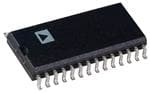
| 描述 | IC DAC 10BIT QUAD VOUT 28-TSSOP数模转换器- DAC Quad 10-Bit |
| 产品分类 | |
| 品牌 | Analog Devices Inc |
| 产品手册 | |
| 产品图片 |
|
| rohs | 符合RoHS无铅 / 符合限制有害物质指令(RoHS)规范要求 |
| 产品系列 | 数据转换器IC,数模转换器- DAC,Analog Devices AD5336BRUZ- |
| 数据手册 | |
| 产品型号 | AD5336BRUZ |
| 产品培训模块 | http://www.digikey.cn/PTM/IndividualPTM.page?site=cn&lang=zhs&ptm=19145http://www.digikey.cn/PTM/IndividualPTM.page?site=cn&lang=zhs&ptm=18614http://www.digikey.cn/PTM/IndividualPTM.page?site=cn&lang=zhs&ptm=26125http://www.digikey.cn/PTM/IndividualPTM.page?site=cn&lang=zhs&ptm=26140http://www.digikey.cn/PTM/IndividualPTM.page?site=cn&lang=zhs&ptm=26150http://www.digikey.cn/PTM/IndividualPTM.page?site=cn&lang=zhs&ptm=26147 |
| 产品目录页面 | |
| 产品种类 | 数模转换器- DAC |
| 位数 | 10 |
| 供应商器件封装 | 28-TSSOP |
| 分辨率 | 10 bit |
| 包装 | 管件 |
| 商标 | Analog Devices |
| 安装类型 | 表面贴装 |
| 安装风格 | SMD/SMT |
| 封装 | Tube |
| 封装/外壳 | 28-TSSOP(0.173",4.40mm 宽) |
| 封装/箱体 | TSSOP-28 |
| 工作温度 | -40°C ~ 105°C |
| 工厂包装数量 | 50 |
| 建立时间 | 7µs |
| 接口类型 | Parallel |
| 数据接口 | 并联 |
| 最大功率耗散 | 4.5 mW |
| 最大工作温度 | + 105 C |
| 最小工作温度 | - 40 C |
| 标准包装 | 50 |
| 电压参考 | External |
| 电压源 | 单电源 |
| 电源电压-最大 | 5.5 V |
| 电源电压-最小 | 2.5 V |
| 积分非线性 | +/- 4 LSB |
| 稳定时间 | 7 us |
| 系列 | AD5336 |
| 结构 | Resistor String |
| 转换器数 | 4 |
| 转换器数量 | 4 |
| 输出数和类型 | 4 电压 |
| 输出类型 | Voltage |
| 采样比 | 143 kSPs |
| 采样率(每秒) | - |


- 商务部:美国ITC正式对集成电路等产品启动337调查
- 曝三星4nm工艺存在良率问题 高通将骁龙8 Gen1或转产台积电
- 太阳诱电将投资9.5亿元在常州建新厂生产MLCC 预计2023年完工
- 英特尔发布欧洲新工厂建设计划 深化IDM 2.0 战略
- 台积电先进制程称霸业界 有大客户加持明年业绩稳了
- 达到5530亿美元!SIA预计今年全球半导体销售额将创下新高
- 英特尔拟将自动驾驶子公司Mobileye上市 估值或超500亿美元
- 三星加码芯片和SET,合并消费电子和移动部门,撤换高东真等 CEO
- 三星电子宣布重大人事变动 还合并消费电子和移动部门
- 海关总署:前11个月进口集成电路产品价值2.52万亿元 增长14.8%


PDF Datasheet 数据手册内容提取
a (cid:1) 2.5 V to 5.5 V, 500 A, Parallel Interface Quad Voltage-Output 8-/10-/12-Bit DACs AD5334/AD5335/AD5336/AD5344* FEATURES GENERAL DESCRIPTION AD5334: Quad 8-Bit DAC in 24-Lead TSSOP The AD5334/AD5335/AD5336/AD5344 are quad 8-, 10-, and AD5335: Quad 10-Bit DAC in 24-Lead TSSOP 12-bit DACs. They operate from a 2.5 V to 5.5 V supply con- AD5336: Quad 10-Bit DAC in 28-Lead TSSOP suming just 500 µA at 3 V, and feature a power-down mode that AD5344: Quad 12-Bit DAC in 28-Lead TSSOP further reduces the current to 80 nA. These devices incorporate Low Power Operation: 500 (cid:1)A @ 3 V, 600 (cid:1)A @ 5 V an on-chip output buffer that can drive the output to both sup- Power-Down to 80 nA @ 3 V, 200 nA @ 5 V via PD Pin ply rails. 2.5 V to 5.5 V Power Supply The AD5334/AD5335/AD5336/AD5344 have a parallel interface. Double-Buffered Input Logic CS selects the device and data is loaded into the input registers Guaranteed Monotonic by Design Over All Codes on the rising edge of WR. Output Range: 0–V or 0–2 V REF REF Power-On Reset to Zero Volts The GAIN pin on the AD5334 and AD5336 allows the output Simultaneous Update of DAC Outputs via LDAC Pin range to be set at 0 V to V or 0 V to 2 × V . REF REF Asynchronous CLR Facility Input data to the DACs is double-buffered, allowing simultaneous Low Power Parallel Data Interface update of multiple DACs in a system using the LDAC pin. On-Chip Rail-to-Rail Output Buffer Amplifiers Temperature Range: –40(cid:2)C to +105(cid:2)C On the AD5334, AD5335 and AD5336 an asynchronous CLR input is also provided. This resets the contents of the Input APPLICATIONS Register and the DAC Register to all zeros. These devices also Portable Battery-Powered Instruments incorporate a power-on-reset circuit that ensures that the DAC Digital Gain and Offset Adjustment output powers on to 0 V and remains there until valid data is Programmable Voltage and Current Sources written to the device. Programmable Attenuators The AD5334/AD5335/AD5336/AD5344 are available in Thin Industrial Process Control Shrink Small Outline Packages (TSSOP). AD5334 FUNCTIONAL BLOCK DIAGRAM (Other Diagrams Inside) VREFA/B VDD POWER-ON AD5334 RESET GAIN DB...7 REINGPISUTTER REGDIASCTER 8D-BAICT BUFFER VOUTA DB0 CS REINGPISUTTER REGDIASCTER 8D-BAICT BUFFER VOUTB WR INTER- FACE A0 LOGIC A1 REINGPISUTTER REGDIASCTER 8D-BA8DIC-TBAICT BUFFER VOUTC REINGPISUTTER REGDIASCTER 8D-BAICT BUFFER VOUTD CLR TO ALL DACS AND BUFFERS LDAC POWER-DOWN LOGIC VREFC/D PD GND *Protected by U.S. Patent Number 5,969,657. REV.0 Information furnished by Analog Devices is believed to be accurate and reliable. However, no responsibility is assumed by Analog Devices for its use, nor for any infringements of patents or other rights of third parties One Technology Way, P.O. Box 9106, Norwood, MA 02062-9106, U.S.A. which may result from its use. No license is granted by implication or Tel: 781/329-4700 World Wide Web Site: http://www.analog.com otherwise under any patent or patent rights of Analog Devices. Fax: 781/326-8703 © Analog Devices, Inc., 2000
AD5334/AD5335/AD5336/AD5344–SPECIFICATIONS (V = 2.5 V to 5.5 V, V = 2 V. R = 2 k(cid:3) to GND; C =200 pF to GND; all specifications T to T unless otherwise noted.) DD REF L L MIN MAX B Version2 Parameter1 Min Typ Max Unit Conditions/Comments DC PERFORMANCE3, 4 AD5334 Resolution 8 Bits Relative Accuracy ±0.15 ±1 LSB Differential Nonlinearity ±0.02 ±0.25 LSB Guaranteed Monotonic By Design Over All Codes AD5335/AD5336 Resolution 10 Bits Relative Accuracy ±0.5 ±4 LSB Differential Nonlinearity ±0.05 ±0.5 LSB Guaranteed Monotonic By Design Over All Codes AD5344 Resolution 12 Bits Relative Accuracy ±2 ±16 LSB Differential Nonlinearity ±0.2 ±1 LSB Guaranteed Monotonic By Design Over All Codes Offset Error ±0.4 ±3 % of FSR Gain Error ±0.1 ±1 % of FSR Lower Deadband5 10 60 mV Lower Deadband Exists Only if Offset Error Is Negative Upper Deadband 10 60 mV V = 5 V. Upper Deadband Exists Only if V V DD REF = DD Offset Error Drift6 –12 ppm of FSR/°C Gain Error Drift6 –5 ppm of FSR/°C DC Power Supply Rejection Ratio6 –60 dB ∆V = ±10% DD DC Crosstalk6 200 µV R = 2 kΩ to GND, 2 kΩ to V ; C = 200 pF to GND; L DD L Gain = 0 DAC REFERENCE INPUT6 V Input Range 0.25 V V REF DD V Input Impedance 180 kΩ Gain = 1. Input Impedance = R (AD5336/AD5344) REF DAC 90 kΩ Gain = 2. Input Impedance = R (AD5336) DAC 90 kΩ Gain = 1. Input Impedance = R (AD5334/AD5335) DAC 45 kΩ Gain = 2. Input Impedance = R (AD5334) DAC Reference Feedthrough –90 dB Frequency = 10 kHz Channel-to-Channel Isolation –90 dB Frequency = 10 kHz OUTPUT CHARACTERISTICS6 Minimum Output Voltage4, 7 0.001 V min Rail-to-Rail Operation Maximum Output Voltage4, 7 V – 0.001 V max DD DC Output Impedance 0.5 Ω Short Circuit Current 50 mA V = 5 V DD 20 mA V = 3 V DD Power-Up Time 2.5 µs Coming Out of Power-Down Mode. V = 5 V DD 5 µs Coming Out of Power-Down Mode. V = 3 V DD LOGIC INPUTS6 Input Current ±1 µA V , Input Low Voltage 0.8 V V = 5 V ± 10% IL DD 0.6 V V = 3 V ± 10% DD 0.5 V V = 2.5 V DD V , Input High Voltage 2.4 V V = 5 V ± 10% IH DD 2.1 V V = 3 V ± 10% DD 2.0 V V = 2.5 V DD Pin Capacitance 3.5 pF POWER REQUIREMENTS V 2.5 5.5 V DD I (Normal Mode) All DACs active and excluding load currents. DD V = 4.5 V to 5.5 V 600 900 µA V = V , V = GND. DD IH DD IL V = 2.5 V to 3.6 V 500 700 µA I increases by 50 µA at V > V – 100 mV. DD DD REF DD I (Power-Down Mode) DD V = 4.5 V to 5.5 V 0.2 1 µA DD V = 2.5 V to 3.6 V 0.08 1 µA DD NOTES 1See Terminology section. 2Temperature range: B Version: –40°C to +105°C; typical specifications are at 25°C. 3Linearity is tested using a reduced code range: AD5334 (Code 8 to 255); AD5335/AD5336 (Code 28 to 1023); AD5344 (Code 115 to 4095). 4DC specifications tested with outputs unloaded. 5This corresponds to x codes. x = Deadband voltage/LSB size. 6Guaranteed by design and characterization, not production tested. 7In order for the amplifier output to reach its minimum voltage, Offset Error must be negative. In order for the amplifier output to reach its maximum voltage, V = V and REF DD “Offset plus Gain” Error must be positive. Specifications subject to change without notice. –2– REV. 0
AD5334/AD5335/AD5336/AD5344 (V = 2.5 V to 5.5 V. R = 2 k(cid:3) to GND; C = 200 pF to GND. All specifications T to T unless other- AC CHARACTERISTICS1 DD L L MIN MAX wise noted.) B Version3 Parameter2 Min Typ Max Unit Conditions/Comments Output Voltage Settling Time V = 2 V. See Figure 20 REF AD5334 6 8 µs 1/4 Scale to 3/4 Scale Change (40 H to C0 H) AD5335 7 9 µs 1/4 Scale to 3/4 Scale Change (100 H to 300 H) AD5336 7 9 µs 1/4 Scale to 3/4 Scale Change (100 H to 300 H) AD5344 8 10 µs 1/4 Scale to 3/4 Scale Change (400 H to C00 H) Slew Rate 0.7 V/µs Major Code Transition Glitch Energy 8 nV-s 1 LSB Change Around Major Carry Digital Feedthrough 0.5 nV-s Digital Crosstalk 3 nV-s Analog Crosstalk 0.5 nV-s DAC-to-DAC Crosstalk 3.5 nV-s Multiplying Bandwidth 200 kHz V = 2 V ± 0.1 V p-p. Unbuffered Mode REF Total Harmonic Distortion –70 dB V = 2.5 V ± 0.1 V p-p. Frequency = 10 kHz REF NOTES 1Guaranteed by design and characterization, not production tested. 2See Terminology section. 3Temperature range: B Version: –40°C to +105°C; typical specifications are at 25°C. Specifications subject to change without notice. TIMING CHARACTERISTICS1, 2, 3 (V = 2.5 V to 5.5 V, All specifications T to T unless otherwise noted.) DD MIN MAX Parameter Limit at T , T Unit Condition/Comments MIN MAX t 0 ns min CS to WR Setup Time 1 t 0 ns min CS to WR Hold Time 2 t 20 ns min WR Pulsewidth 3 t 5 ns min Data, GAIN, HBEN Setup Time 4 t 4.5 ns min Data, GAIN, HBEN Hold Time 5 t 5 ns min Synchronous Mode. WR Falling to LDAC Falling. 6 t 5 ns min Synchronous Mode. LDAC Falling to WR Rising. 7 t 4.5 ns min Synchronous Mode. WR Rising to LDAC Rising. 8 t 5 ns min Asynchronous Mode. LDAC Rising to WR Rising. 9 t 4.5 ns min Asynchronous Mode. WR Rising to LDAC Falling. 10 t 20 ns min LDAC Pulsewidth 11 t 20 ns min CLR Pulsewidth 12 t 50 ns min Time Between WR Cycles 13 t 20 ns min A0, A1 Setup Time 14 t 0 ns min A0, A1 Hold Time 15 NOTES 1Guaranteed by design and characterization, not production tested. 2All input signals are specified with tr = tf = 5 ns (10% to 90% of V ) t1 t2 DD and timed from a voltage level of (V + V )/2. CS IL IH 3See Figure 1. t t 3 13 Specifications subject to change without notice. WR t 5 t DATA, 4 GAIN, HBEN t6 t t8 7 LDAC1 t t t 9 10 11 LDAC2 t 12 CLR t14 t15 A0, A1 NOTES: 1 SYNCHRONOUS LDAC UPDATE MODE 2 ASYNCHRONOUS LDAC UPDATE MODE Figure 1.Parallel Interface Timing Diagram REV. 0 –3–
AD5334/AD5335/AD5336/AD5344 ABSOLUTE MAXIMUM RATINGS* Reflow Soldering (T = 25°C unless otherwise noted) Peak Temperature . . . . . . . . . . . . . . . . . . . . . .220 +5/–0°C A V to GND . . . . . . . . . . . . . . . . . . . . . . . . . . –0.3 V to +7 V Time at Peak Temperature . . . . . . . . . . . . .10 sec to 40 sec DD Digital Input Voltage to GND . . . . . . . .–0.3 V to VDD + 0.3 V *Stresses above those listed under Absolute Maximum Ratings may cause perma- Digital Output Voltage to GND . . . . . .–0.3 V to V + 0.3 V nent damage to the device. This is a stress rating only; functional operation of the DD Reference Input Voltage to GND . . . . –0.3 V to V + 0.3 V device at these or any other conditions above those listed in the operational DD sections of this specification is not implied. Exposure to absolute maximum rating V to GND . . . . . . . . . . . . . . . . . . . –0.3 V to V + 0.3 V OUT DD conditions for extended periods may affect device reliability. Operating Temperature Range Industrial (B Version) . . . . . . . . . . . . . . . –40°C to +105°C Storage Temperature Range . . . . . . . . . . . . –65°C to +150°C Junction Temperature . . . . . . . . . . . . . . . . . . . . . . . . . .150°C TSSOP Package Power Dissipation . . . . . . . . . . . . . . . (T max – T )/θ mW J A JA θ Thermal Impedance (24-Lead TSSOP) . . . . . 128°C/W JA θ Thermal Impedance (28-Lead TSSOP) . . . . . 97.9°C/W JA θ Thermal Impedance (24-Lead TSSOP) . . . . . . 42°C/W JC θ Thermal Impedance (28-Lead TSSOP) . . . . . . 14°C/W JC ORDERING GUIDE Model Temperature Range Package Description Package Option AD5334BRU –40°C to +105°C TSSOP (Thin Shrink Small Outline Package) RU-24 AD5335BRU –40°C to +105°C TSSOP (Thin Shrink Small Outline Package) RU-24 AD5336BRU –40°C to +105°C TSSOP (Thin Shrink Small Outline Package) RU-28 AD5344BRU –40°C to +105°C TSSOP (Thin Shrink Small Outline Package) RU-28 CAUTION ESD (electrostatic discharge) sensitive device. Electrostatic charges as high as 4000 V readily WARNING! accumulate on the human body and test equipment and can discharge without detection. Although the AD5334/AD5335/AD5336/AD5344 features proprietary ESD protection circuitry, permanent damage may occur on devices subjected to high-energy electrostatic discharges. Therefore, proper ESD precautions are recommended to avoid performance degradation or loss of functionality. ESD SENSITIVE DEVICE –4– REV. 0
AD5334/AD5335/AD5336/AD5344 AD5334 FUNCTIONAL BLOCK DIAGRAM AD5334 PIN CONFIGURATION VREFA/B VDD VREFC/D 1 24 CLR PORWEESRE-TON AD5334 VREFA/B 2 23 GAIN VOUTA 3 22 DB7 GAIN DB...7 REINGPISUTTER REGDIASCTER 8D-ABICT BUFFER VOUTA VVOOUUTTBC 45 AD85-B3I3T4 2210 DDBB65 DB0 VOUTD 6 TOP VIEW 19 DB4 CS GND 7 (Not to Scale) 18 DB3 REINGPISUTTER REGDIASCTER 8D-ABICT BUFFER VOUTB CS 8 17 DB2 WR INTER- WR 9 16 DB1 A0 LFOAGCIEC A0 10 15 DB0 A1 11 14 VDD A1 REINGPISUTTER REGDIASCTER 8D-BA8DIC-TABICT BUFFER VOUTC LDAC 12 13 PD REINGPISUTTER REGDIASCTER 8D-ABICT BUFFER VOUTD CLR TO ALL DACS AND BUFFERS LDAC POWER-DOWN LOGIC VREFC/D PD GND AD5334 PIN FUNCTION DESCRIPTIONS Pin No. Mnemonic Function 1 V C/D Unbuffered Reference Input for DACs C and D. REF 2 V A/B Unbuffered Reference Input for DACs A and B. REF 3 V A Output of DAC A. Buffered Output with Rail-to-Rail Operation. OUT 4 V B Output of DAC B. Buffered Output with Rail-to-Rail Operation. OUT 5 V C Output of DAC C. Buffered Output with Rail-to-Rail Operation. OUT 6 V D Output of DAC D. Buffered Output with Rail-to-Rail Operation. OUT 7 GND Ground Reference Point for All Circuitry on the Part. 8 CS Active Low Chip Select Input. This is used in conjunction with WR to write data to the parallel interface. 9 WR Active Low Write Input. This is used in conjunction with CS to write data to the parallel interface. 10 A0 LSB Address Pin for Selecting which DAC Is to Be Written to. 11 A1 MSB Address Pin for Selecting which DAC Is to Be Written to. 12 LDAC Active Low Control Input that Updates the DAC Registers with the Contents of the Input Registers. This allows all DAC outputs to be simultaneously updated. 13 PD Power-Down Pin. This active low control pin puts all DACs into power-down mode. 14 V Power Supply Pin. This part can operate from 2.5 V to 5.5 V and the supply should be decoupled with a DD 10µF capacitor in parallel with a 0.1µF capacitor to GND. 15–22 DB –DB Eight Parallel Data Inputs. DB is the MSB of these eight bits. 0 7 7 23 GAIN Gain Control Pin. This controls whether the output range from the DAC is 0–V or 0–2 V REF REF 24 CLR Asynchronous Active Low Control Input that Clears All Input Registers and DAC Registers to Zeros. REV. 0 –5–
AD5334/AD5335/AD5336/AD5344 AD5335 FUNCTIONAL BLOCK DIAGRAM AD5335 PIN CONFIGURATION VREFA/B VDD POWER-ON VREFC/D 1 24 CLR RESET VREFA/B 2 23 HBEN AD5335 HIGH BYTE VOUTA 3 22 DB7 REGISTER VOUTB 4 21 DB6 10-BIT DD......BB70 LROEWGI SBTYETRE REGDIASCTER 1D0-ABCIT BUFFER VOUTA VVOOGUUNTTDDC 567 (NTAoOtD Pt5o V 3SI3Ec5aWle) 211098 DDDBBB345 CS 8 17 DB2 CS HIGH BYTE WR 9 16 DB1 WR REGISTER A0 10 15 DB0 A1 11 14 VDD A0 INTER- LROEWGI SBTYETRE REGDIASCTER 1D0-ABCIT BUFFER VOUTB LDAC 12 13 PD A1 FACE LOGIC HBEN HIGH BYTE REGISTER LROEWGI SBTYETRE REGDIASCTER 1D0-ABCIT BUFFER VOUTC HIGH BYTE REGISTER LROEWGI SBTYETRE REGDIASCTER 1D0-ABCIT BUFFER VOUTD RESET TO ALL DACS CLR AND BUFFERS LDAC POWER-DOWN LOGIC VREFC/D PD GND AD5335 PIN FUNCTION DESCRIPTIONS Pin No. Mnemonic Function 1 V C/D Unbuffered Reference Input for DACs C and D. REF 2 V A/B Unbuffered Reference Input for DACs A and B. REF 3 V A Output of DAC A. Buffered output with rail-to-rail operation. OUT 4 V B Output of DAC B. Buffered output with rail-to-rail operation. OUT 5 V C Output of DAC C. Buffered output with rail-to-rail operation. OUT 6 V D Output of DAC D. Buffered output with rail-to-rail operation. OUT 7 GND Ground Reference Point for All Circuitry on the Part. 8 CS Active Low Chip Select Input. This is used in conjunction with WR to write data to the parallel interface. 9 WR Active Low Write Input. This is used in conjunction with CS to write data to the parallel interface. 10 A0 LSB Address Pin for Selecting which DAC Is to Be Written to. 11 A1 MSB Address Pin for Selecting which DAC Is to Be Written to. 12 LDAC Active Low Control Input that Updates the DAC Registers with the Contents of the Input Registers. This allows all DAC outputs to be simultaneously updated. 13 PD Power-Down Pin. This active low control pin puts all DACs into power-down mode. 14 V Power Supply Pin. This part can operate from 2.5 V to 5.5 V and the supply should be decoupled with a DD 10µF capacitor in parallel with a 0.1µF capacitor to GND. 15–22 DB –DB Eight Parallel Data Inputs. DB is the MSB of these eight bits. 0 7 7 23 HBEN This pin is used when writing to the device to determine if data is written to the high byte register or the low byte register. 24 CLR Asynchronous Active Low Control Input that Clears All Input Registers and DAC Registers to Zeros. –6– REV. 0
AD5334/AD5335/AD5336/AD5344 AD5336 FUNCTIONAL BLOCK DIAGRAM AD5336 PIN CONFIGURATION VREFA VREFB VDD VREFD 1 28 CLR PORWEESRE-TON AD5336 VREFC 2 27 GAIN VREFB 3 26 DB9 GAIN DB...9 REINGPISUTTER REGDIASCTER 1D0-ABCIT BUFFER VOUTA VVORUEFTAA 45 10-BIT 2254 DDBB87 DB0 VOUTB 6 AD5336 23 DB6 CS VOUTC 7 TOP VIEW 22 DB5 REINGPISUTTER REGDIASCTER 1D0-ABCIT BUFFER VOUTB VOUTD 8 (Not to Scale) 21 DB4 WR INTER- GND 9 20 DB3 A0 LFOAGCIEC CS 10 19 DB2 WR 11 18 DB1 A1 REINGPISUTTER REGDIASCTER 1D0-ABCIT BUFFER VOUTC A0 12 17 DB0 A1 13 16 VDD LDAC 14 15 PD REINGPISUTTER REGDIASCTER 1D0-ABCIT BUFFER VOUTD CLR TO ALL DACS RESET AND BUFFERS LDAC POWER-DOWN LOGIC VREFD VREFC PD GND AD5336 PIN FUNCTION DESCRIPTIONS Pin No. Mnemonic Function 1 V D Unbuffered Reference Input for DAC D. REF 2 V C Unbuffered Reference Input for DAC C. REF 3 V B Unbuffered Reference Input for DAC B. REF 4 V A Unbuffered Reference Input for DAC A. REF 5 V A Output of DAC A. Buffered output with rail-to-rail operation. OUT 6 V B Output of DAC B. Buffered output with rail-to-rail operation. OUT 7 V C Output of DAC C. Buffered output with rail-to-rail operation. OUT 8 V D Output of DAC D. Buffered output with rail-to-rail operation. OUT 9 GND Ground Reference Point for All Circuitry on the Part. 10 CS Active Low Chip Select Input. This is used in conjunction with WR to write data to the parallel interface. 11 WR Active Low Write Input. This is used in conjunction with CS to write data to the parallel interface. 12 A0 LSB Address Pin for Selecting which DAC Is to Be Written to. 13 A1 MSB Address Pin for Selecting which DAC is to Be Written to. 14 LDAC Active Low Control Input that Updates the DAC Registers with the Contents of the Input Registers. This allows all DAC outputs to be simultaneously updated. 15 PD Power-Down Pin. This active low control pin puts all DACs into power-down mode. 16 V Power Supply Pin. This part can operate from 2.5 V to 5.5 V and the supply should be decoupled with a DD 10µF capacitor in parallel with a 0.1µF capacitor to GND. 17–26 DB –DB 10 Parallel Data Inputs. DB is the MSB of these 10 bits. 0 9 9 27 GAIN Gain Control Pin. This controls whether the output range from the DAC is 0–V or 0–2 V . REF REF 28 CLR Asynchronous Active Low Control Input that Clears All Input Registers and DAC Registers to Zeros. REV. 0 –7–
AD5334/AD5335/AD5336/AD5344 AD5344 FUNCTIONAL BLOCK DIAGRAM AD5344 PIN CONFIGURATION VREFA VREFB VDD VREFD 1 28 DB11 POWER-ON AD5344 VREFC 2 27 DB10 RESET VREFB 3 26 DB9 DDB......B101 REINGPISUTTER REGDIASCTER 1D2-ABCIT BUFFER VOUTA VVVOORUUETFTAAB 456 A1D2-5B3I4T4 222543 DDDBBB876 VOUTC 7 TOP VIEW 22 DB5 WCRS REINGPISUTTER REGDIASCTER 1D2-ABCIT BUFFER VOUTB VOGUNTDD 89 (Not to Scale) 2210 DDBB34 INFATECRE- CS 10 19 DB2 A0 LOGIC WR 11 18 DB1 A1 REINGPISUTTER REGDIASCTER 1D2-ABCIT BUFFER VOUTC AA10 1123 1176 VDDBD0 LDAC 14 15 PD REINGPISUTTER REGDIASCTER 1D2-ABCIT BUFFER VOUTD TO ALL DACS AND BUFFERS LDAC POWER-DOWN LOGIC VREFD VREFC PD GND AD5344 PIN FUNCTION DESCRIPTIONS Pin No. Mnemonic Function 1 V D Unbuffered Reference Input for DAC D. REF 2 V C Unbuffered Reference Input for DAC C. REF 3 V B Unbuffered Reference Input for DAC B. REF 4 V A Unbuffered Reference Input for DAC A. REF 5 V A Output of DAC A. Buffered output with rail-to-rail operation. OUT 6 V B Output of DAC B. Buffered output with rail-to-rail operation. OUT 7 V C Output of DAC C. Buffered output with rail-to-rail operation. OUT 8 V D Output of DAC D. Buffered output with rail-to-rail operation. OUT 9 GND Ground Reference Point for All Circuitry on the Part. 10 CS Active Low Chip Select Input. This is used in conjunction with WR to write data to the parallel interface. 11 WR Active Low Write Input. This is used in conjunction with CS to write data to the parallel interface. 12 A0 LSB Address Pin for Selecting which DAC Is to Be Written to. 13 A1 MSB Address Pin for Selecting which DAC Is to Be Written to. 14 LDAC Active Low Control Input that Updates the DAC Registers with the Contents of the Input Registers. This allows all DAC outputs to be simultaneously updated. 15 PD Power-Down Pin. This active low control pin puts all DACs into power-down mode. 16 V Power Supply Pin. This part can operate from 2.5 V to 5.5 V and the supply should be decoupled with a DD 10µF capacitor in parallel with a 0.1µF capacitor to GND. 17–28 DB –DB 12 Parallel Data Inputs. DB is the MSB of these 12 bits. 0 11 11 –8– REV. 0
AD5334/AD5335/AD5336/AD5344 TERMINOLOGY RELATIVE ACCURACY For the DAC, Relative Accuracy or Integral Nonlinearity (INL) GAIN ERROR AND is a measure of the maximum deviation, in LSBs, from a straight OFFSET ERROR line passing through the actual endpoints of the DAC transfer function. Typical INL versus Code plot can be seen in Figures 5, 6, and 7. ACTUAL DIFFERENTIAL NONLINEARITY OUTPUT Differential Nonlinearity (DNL) is the difference between the VOLTAGE IDEAL measured change and the ideal 1 LSB change between any two adjacent codes. A specified differential nonlinearity of ±1 LSB maximum ensures monotonicity. This DAC is guaranteed mono- tonic by design. Typical DNL versus Code plot can be seen in Figures 8, 9, and 10. POSITIVE OFFSET OFFSET ERROR This is a measure of the offset error of the DAC and the output DAC CODE amplifier. It is expressed as a percentage of the full-scale range. Figure 3.Positive Offset Error and Gain Error If the offset voltage is positive, the output voltage will still be positive at zero input code. This is shown in Figure 3. Because the DACs operate from a single supply, a negative offset cannot appear at the output of the buffer amplifier. Instead, there will GAIN ERROR be a code close to zero at which the amplifier output saturates AND (amplifier footroom). Below this code there will be a deadband OFFSET ERROR over which the output voltage will not change.This is illustrated IDEAL in Figure 4. OUTPUT VOLTAGE GAIN ERROR This is a measure of the span error of the DAC (including any ACTUAL error in the gain of the buffer amplifier). It is the deviation in slope of the actual DAC transfer characteristic from the ideal expressed as a percentage of the full-scale range. This is illus- trated in Figure 2. NEGATIVE DAC CODE OFFSET POSITIVE GAIN ERROR NEGATIVE ACTUAL GAIN ERROR DEADBAND CODES AMPLIFIER OUTPUT FOOTROOM VOLTAGE (~1mV) IDEAL NEGATIVE OFFSET DAC CODE Figure 4.Negative Offset Error and Gain Error Figure 2.Gain Error REV. 0 –9–
AD5334/AD5335/AD5336/AD5344 OFFSET ERROR DRIFT DIGITAL FEEDTHROUGH This is a measure of the change in Offset Error with changes in Digital Feedthrough is a measure of the impulse injected into temperature. It is expressed in (ppm of full-scale range)/°C. the analog output of the DAC from the digital input pins of the device but is measured when the DAC is not being written to GAIN ERROR DRIFT (CS held high). It is specified in nV-secs and is measured with a This is a measure of the change in Gain Error with changes in full-scale change on the digital input pins, i.e. from all 0s to all temperature. It is expressed in (ppm of full-scale range)/°C. 1s and vice versa. DC POWER-SUPPLY REJECTION RATIO (PSRR) DIGITAL CROSSTALK This indicates how the output of the DAC is affected by changes in This is the glitch impulse transferred to the output of one DAC the supply voltage. PSRR is the ratio of the change in V to a at midscale in response to a full-scale code change (all 0s to all OUT change in V for full-scale output of the DAC. It is measured 1s and vice versa) in the input register of another DAC. It is DD in dBs. V is held at 2 V and V is varied ±10%. expressed in nV secs. REF DD DC CROSSTALK ANALOG CROSSTALK This is the dc change in the output level of one DAC at mid- This is the glitch impulse transferred to the output of one DAC scale in response to a full-scale code change (all 0s to all 1s and due to a change in the output of another DAC. It is measured vice versa) and output change of another DAC. It is expressed by loading one of the input registers with a full-scale code change in µV. (all 0s to all 1s and vice versa) while keeping LDAC high. Then pulse LDAC low and monitor the output of the DAC whose REFERENCE FEEDTHROUGH digital code was not changed. The area of the glitch is expressed This is the ratio of the amplitude of the signal at the DAC output in nV secs. to the reference input when the DAC output is not being updated (i.e., LDAC is high). It is expressed in dBs. DAC-TO-DAC CROSSTALK This is the glitch impulse transferred to the output of one DAC CHANNEL-TO-CHANNEL ISOLATION due to a digital code change and subsequent output change of This is a ratio of the amplitude of the signal at the output of one another DAC. This includes both digital and analog crosstalk. It DAC to a sine wave on the reference inputs of the other DACs. is measured by loading one of the DACs with a full-scale code It is measured by grounding one V pin and applying a 10kHz, change (all 0s to all 1s and vice versa) with the LDAC pin set REF 4V peak-to-peak sine wave to the other V pins. It is expressed low and monitoring the output of another DAC. The energy of REF in dBs. the glitch is expressed in nV secs. MAJOR-CODE TRANSITION GLITCH ENERGY MULTIPLYING BANDWIDTH Major-Code Transition Glitch Energy is the energy of the The amplifiers within the DAC have a finite bandwidth. The impulse injected into the analog output when the DAC changes Multiplying Bandwidth is a measure of this. A sine wave on the state. It is normally specified as the area of the glitch in nV secs reference (with full-scale code loaded to the DAC) appears on and is measured when the digital code is changed by 1 LSB at the output. The Multiplying Bandwidth is the frequency at which the major carry transition (011...11 to 100...00 or 100...00 the output amplitude falls to 3 dB below the input. to 011...11). TOTAL HARMONIC DISTORTION This is the difference between an ideal sine wave and its attenuated version using the DAC. The sine wave is used as the reference for the DAC and the THD is a measure of the harmonics present on the DAC output. It is measured in dBs. –10– REV. 0
Typical Performance Characteristics–AD5334/AD5335/AD5336/AD5344 1.0 3 12 TVAD D= =2 55(cid:2)VC 2 TVAD D= =2 55(cid:2)VC 8 TVAD D= =2 55(cid:2)VC 0.5 OR – LSBs 0 OR – LSBs 01 OR – LSBs 04 R R R R R R NL E NL E –1 NL E –4 I–0.5 I I –2 –8 –1.0 –3 –12 0 50 100 150 200 250 0 200 400 600 800 1000 0 1000 2000 3000 4000 CODE CODE CODE Figure 5.AD5334 Typical INL Plot Figure 6.AD5335 Typical INL Plot Figure 7.AD5336 Typical INL Plot 0.3 TA = 25(cid:2)C 0.6 TA = 25(cid:2)C 1 TA = 25(cid:2)C 0.2 VDD = 5V 0.4 VDD = 5V VDD = 5V 0.5 DNL ERROR – LSBs–00..110 DNL ERROR – LSBs–00..022 DNL ERROR – LSBs 0 –0.5 –0.2 –0.4 –0.3 –0.6 –1 0 50 100 150 200 250 0 200 400 600 800 1000 0 1000 2000 3000 4000 CODE CODE CODE Figure 8.AD5334 Typical DNL Plot Figure 9.AD5335 Typical DNL Plot Figure 10.AD5336 Typical DNL Plot 0.5 0.5 1 VDD = 5V 0.4 VDD = 5V VDD = 5V TA = 25(cid:2)C MAX INL 0.3 VREF = 2V MAX INL VREF = 2V 0.25 0.5 0.2 ERROR – LSBs 0 MIN DNL MAX DNL ERROR – LSBs–00..011 MAX DNL MIN DNL ERROR – % 0 GAIN ERROOFRFSET ERROR –0.2 –0.25 –0.5 –0.3 MIN INL MIN INL –0.4 –0.50 1 2 3 4 5 –0.5(cid:4)40 0 40 80 120 –1(cid:4)40 0 40 80 120 VREF – V TEMPERATURE – (cid:2)C TEMPERATURE – (cid:2)C Figure 11.AD5334 INL and DNL Figure 12.AD5334 INL Error and Figure 13.AD5334 Offset Error Error vs. V DNL Error vs. Temperature and Gain Error vs. Temperature REF REV. 0 –11–
AD5334/AD5335/AD5336/AD5344 0.2 5 600 0.1 TVAR E=F 2=5 2(cid:2)CV 4 5V SOURCE 500 VDD = 5.5V 0 GAIN ERROR 3V SOURCE 400 VDD = 3.6V ROR – %––00..21 – VoltsUT 3 (cid:1)I – ADD300 R O 2 E–0.3 V 200 TA = 25(cid:2)C –0.4 OFFSET ERROR VREF = 2V 1 3V SINK 100 –0.5 5V SINK 0 –0.6 0 ZERO-SCALE FULL SCALE 0 1 2 3 4 5 6 0 1 2 3 4 5 6 DAC CODE VDD – Volts SINK/SOURCE CURRENT – mA Figure 14.Offset Error and Gain Figure 15.V Source and Sink Figure 16.Supply Current OUT Error vs. V Current Capability vs. DAC Code DD 600 0.5 1800 TA = 25(cid:2)C TA = 25(cid:2)C 1600 500 0.4 1400 400 1200 (cid:1)A (cid:1)A0.3 (cid:1)A1000 – DD300 – DD – DD 800 I I0.2 I 200 600 VDD = 5V 400 100 0.1 VDD = 3V 200 0 0 0 2.5 3.0 3.5 4.0 4.5 5.0 5.5 2.5 3.0 3.5 4.0 4.5 5.0 5.5 0 1 2 3 4 5 VDD – V VDD– V VLOGIC – V Figure 17.Supply Current vs. Supply Figure 18.Power-Down Current vs. Figure 19.Supply Current Voltage Supply Voltage vs. Logic Input Voltage TA = 255(cid:2)µCs TA = 25(cid:2)C TA = 25(cid:2)C VDD = 5V VDD = 5V VDD = 5V CH1 VREF = 5V CH1 VREF = 2V VREF = 2V VOUTA VDD CH1 VOUTA LDAC VOUTA PD CH2 CH2 CH2 CH1 1V, CH2 5V, TIME BASE= 1(cid:1)s/DIV CH1 2V, CH2 200mV, TIME BASE = 200(cid:1)s/DIV CH1 500mV, CH2 5V, TIME BASE = 1(cid:1)s/DIV Figure 20.Half-Scale Settling (1/4 to Figure 21.Power-On Reset to 0 V Figure 22.Exiting Power-Down 3/4 Scale Code Change) to Midscale –12– REV. 0
AD5334/AD5335/AD5336/AD5344 0.929 10 0.928 0 0.927 VDD = 3V VDD = 5V 0.926 –10 FREQUENCY V – VoltsOUT 000...999222345 dB ––2300 0.922 –40 0.921 –50 0.920 0.919 –60 300 350 400 450 500 550 600 500ns/DIV 0.01 0.1 1 10 100 1k 10k IDD – (cid:1)A FREQUENCY – kHz Figure 23.I Histogram with V = Figure 24.AD5344 Major-Code Tran- Figure 25.Multiplying Bandwidth DD DD 3 V and V = 5 V sition Glitch Energy (Small-Signal Frequency Response) DD 0.4 VDD = 5V R 0.3 TA = 25(cid:2)C S F % – 0.2 R O E ERR 0.1 mV/DIV AL 1 C 0 S L- L U F–0.1 –0.2 0 1 2 3 4 5 6 VREF – V 750ns/DIV Figure 26.Full-Scale Error vs. V Figure 27.DAC-DAC Crosstalk REF FUNCTIONAL DESCRIPTION where: The AD5334/AD5335/AD5336/AD5344 are quad resistor- D = decimal equivalent of the binary code which is loaded to string DACs fabricated on a CMOS process with resolutions of the DAC register: 8, 10, 10, and 12 bits, respectively. They are written to using a parallel interface. They operate from single supplies of 2.5 V to 0–255 for AD5334 (8 Bits) 5.5V and the output buffer amplifiers offer rail-to-rail output 0–1023 for AD5335/AD5336 (10 Bits) swing. The gain of the buffer amplifiers in the AD5334 and 0–4095 for AD5344 (12 Bits) AD5336 can be set to 1 or 2 to give an output voltage range of N = DAC resolution 0 to V or 0 to 2 V . The AD5335 and AD5344 have out- REF REF put buffers with unity gain. Gain = Output Amplifier Gain (1 or 2) The devices have a power-down feature that reduces current VREF consumption to only 80 nA @ 3 V. GAIN Digital-to-Analog Section Tbuhfefe arr acnhdit eac truerseis toofr o-snteri nDgA DCA cCh afnonlleolw ceodn sbiys tas no fo ua trpeufet rbeunfcfeer REINGPISUTTER REGDIASCTER RSETSRISINTOGR VOUT amplifier. The voltage at the V pin provides the reference OUTPUT REF voltage for the DAC. Figure 28 shows a block diagram of the BUFFER AMPLIFIER DAC architecture. Since the input coding to the DAC is Figure 28.Single DAC Channel Architecture straight binary, the ideal output voltage is given by: D V =V × ×Gain OUT REF 2N REV. 0 –13–
AD5334/AD5335/AD5336/AD5344 Resistor String Access to the DAC register is controlled by the LDAC function. The resistor string section is shown in Figure 29. It is simply a When LDAC is high, the DAC register is latched and the input string of resistors, each of value R. The digital code loaded register may change state without affecting the contents of the to the DAC register determines at what node on the string the DAC register. However, when LDAC is brought low, the DAC voltage is tapped off to be fed into the output amplifier. The register becomes transparent and the contents of the input voltage is tapped off by closing one of the switches connecting register are transferred to it. The gain control signal is also the string to the amplifier. Because it is a string of resistors, it is double-buffered and is only updated when LDAC is taken low. guaranteed monotonic. This is useful if the user requires simultaneous updating of all DACs and peripherals. The user may write to all input registers VREF individually and then, by pulsing the LDAC input low, all out- R puts will update simultaneously. Double-buffering is also useful where the DAC data is loaded in R two bytes, as in the AD5335, because it allows the whole data word to be assembled in parallel before updating the DAC register. TO OUTPUT R AMPLIFIER This prevents spurious outputs that could occur if the DAC register were updated with only the high byte or the low byte. These parts contain an extra feature whereby the DAC register is not updated unless its input register has been updated since R the last time that LDAC was brought low. Normally, when LDAC is brought low, the DAC registers are filled with the R contents of the input registers. In the case of the AD5334/ AD5335/AD5336/AD5344, the part will only update the DAC register if the input register has been changed since the last Figure 29.Resistor String time the DAC register was updated. This removes unnecessary DAC Reference Input crosstalk. The DACs operate with an external reference. The reference Clear Input (CLR) inputs are unbuffered and have an input range of 0.25 V to V . DD CLR is an active low, asynchronous clear that resets the input and The impedance per DAC is typically 180 kΩ for 0–V mode REF DAC registers. Note that the AD5344 has no CLR function. and 90 kΩ for 0–2 V mode. The AD5336 and AD5344 have REF separate reference inputs for each DAC, while the AD5334 and Chip Select Input (CS) AD5335 have a reference inputs for each pair of DACS (A/B CS is an active low input that selects the device. and C/D). Write Input (WR) Output Amplifier WR is an active low input that controls writing of data to the The output buffer amplifier is capable of generating output device. Data is latched into the input register on the rising edge voltages to within 1 mV of either rail. Its actual range depends of WR. on VREF, GAIN, the load on VOUT, and offset error. Load DAC Input (LDAC) If a gain of 1 is selected (GAIN = 0), the output range is 0.001 V LDAC transfers data from the input register to the DAC register to V . (and hence updates the outputs). Use of the LDAC function REF enables double buffering of the DAC and GAIN data. There If a gain of 2 is selected (GAIN = 1), the output range is 0.001 V are two LDAC modes: to 2 V . However because of clamping the maximum output REF is limited to V – 0.001 V. Synchronous Mode: In this mode the DAC register is updated DD after new data is read in on the rising edge of the WR input. The output amplifier is capable of driving a load of 2 kΩ to LDAC can be tied permanently low or pulsed as in Figure 1. GND or V , in parallel with 500 pF to GND or V . The DD DD source and sink capabilities of the output amplifier can be seen Asynchronous Mode: In this mode the outputs are not updated in Figure 15. at the same time that the input register is written to. When LDAC goes low the DAC register is updated with the contents of the The slew rate is 0.7 V/µs with a half-scale settling time to ±0.5 LSB input register. (at 8 bits) of 6 µs with the output unloaded. See Figure 20. High-Byte Enable Input (HBEN) PARALLEL INTERFACE High-Byte Enable is a control input on the AD5335 only that The AD5334, AD5336, and AD5344 load their data as a single determines if data is written to the high-byte input register or 8-, 10-, or 12-bit word, while the AD5335 loads data as a low the low-byte input register. byte of 8 bits and a high byte containing 2 bits. The low data byte of the AD5335 consists of data bits 0 to 7 at Double-Buffered Interface data inputs DB0 to DB7, while the high byte consists of Data The AD5334/AD5335/AD5336/AD5344 DACs all have double- Bits 8 and 9 at data inputs DB and DB . DB to DB are 0 1 2 7 buffered interfaces consisting of an input register and a DAC ignored during a high byte write. See Figure 30. register. DAC data and GAIN inputs (when available) are written to the input register under control of the Chip Select (CS) and Write (WR). –14– REV. 0
AD5334/AD5335/AD5336/AD5344 When the PD pin is high, the DACs work normally with a typical HIGH BYTE power consumption of 600 µA at 5 V (500 µA at 3 V). In power- X X X X X X DB9 DB8 down mode, however, the supply current falls to 200 nA at 5 V LOW BYTE (80 nA at 3 V) when the DACs are powered down. Not only DB7 DB6 DB5 DB4 DB3 DB2 DB1 DB0 does the supply current drop, but the output stage is also internally X = UNUSED BIT switched from the output of the amplifier, making it open-circuit. Figure 30.Data Format For AD5335 This has the advantage that the outputs are three-state while the part is in power-down mode, and provides a defined input POWER-ON RESET condition for whatever is connected to the outputs of the The AD5334/AD5335/AD5336/AD5344 are provided with a DAC amplifiers. The output stage is illustrated in Figure 31. power-on reset function, so that they power up in a defined state. The power-on state is: • Normal operation • 0 – VREF output range SRTERSINISGT DOARC AMPLIFIER VOUT • Output voltage set to 0 V POWER-DOWN Both input and DAC registers are filled with zeros and remain CIRCUITRY so until a valid write sequence is made to the device. This is particularly useful in applications where it is important to know Figure 31. Output Stage During Power-Down the state of the DAC outputs while the device is powering up. The bias generator, the output amplifier, the resistor string, and all other associated linear circuitry are all shut down when the POWER-DOWN MODE power-down mode is activated. However, the contents of the The AD5334/AD5335/AD5336/AD5344 have low power con- registers are unaffected when in power-down. The time to exit sumption, dissipating typically 1.5 mW with a 3 V supply and power-down is typically 2.5 µs for V = 5 V and 5 µs when 3 mW with a 5 V supply. Power consumption can be further DD V = 3 V. This is the time from a rising edge on the PD pin reduced when the DACs are not in use by putting them into DD to when the output voltage deviates from its power-down volt- power-down mode, which is selected by taking pin PD low. age. See Figure 22. Table I. AD5334/AD5336/AD5344 Truth Table CLR LDAC CS WR A1 A0 Function 1 1 1 X X X No Data Transfer 1 1 X 1 X X No Data Transfer 0 X X X X X Clear All Registers 1 1 0 0➝1 0 0 Load DAC A Input Register, GAIN A (AD5334/AD5336) 1 1 0 0➝1 0 1 Load DAC B Input Register, GAIN B (AD5334/AD5336) 1 1 0 0➝1 1 0 Load DAC C Input Register, GAIN C (AD5334/AD5336) 1 1 0 0➝1 1 1 Load DAC D Input Register, GAIN D (AD5334/AD5336) 1 0 X X X X Update DAC Registers X = don’t care. Table II. AD5335 Truth Table CLR LDAC CS WR A1 A0 HBEN Function 1 1 1 X X X X No Data Transfer 1 1 X 1 X X X No Data Transfer 0 X X X X X X Clear All Registers 1 1 0 0➝1 0 0 0 Load DAC A Low Byte Input Register 1 1 0 0➝1 0 0 1 Load DAC A High Byte Input Register 1 1 0 0➝1 0 1 0 Load DAC B Low Byte Input Register 1 1 0 0➝1 0 1 1 Load DAC B High Byte Input Register 1 1 0 0➝1 1 0 0 Load DAC C Low Byte Input Register 1 1 0 0➝1 1 0 1 Load DAC C High Byte Input Register 1 1 0 0➝1 1 1 0 Load DAC D Low Byte Input Register 1 1 0 0➝1 1 1 1 Load DAC D High Byte Input Register 1 0 X X X X X Update DAC Registers X = don’t care. REV. 0 –15–
AD5334/AD5335/AD5336/AD5344 SUGGESTED DATABUS FORMATS 6V TO 16V In many applications the GAIN input of the AD5334 and AD5336 may be hard-wired. However, if more flexibility is required, it can be included in a data bus. This enables the user 0.1(cid:1)F 10(cid:1)F to software program GAIN, giving the option of doubling the resolution in the lower half of the DAC range. In a bused system VIN GAIN may be treated as a data input since it is written to the ADM663/ADM666 device during a write operation and takes effect when LDAC is taken low. This means that the output amplifier gain of multiple SENSE VDD DAC devices can be controlled using a common GAIN line. VOUT(2) VREF* VOUT* VSET GNDSHDN 0.1(cid:1)F AD5334/AD5335/ The AD5336 databus must be at least 10 bits wide and is best AD5336/AD5344 suited to a 16-bit databus system. Examples of data formats for putting GAIN on a 16-bit databus GND are shown in Figure 32. Note that any unused bits above the actual DAC data may be used for GAIN. *ONLY ONE CHANNEL OF VREF AND VOUT SHOWN Figure 34. Using an ADM663/ADM666 as Power and AD5336 Reference to AD5334/AD5335/AD5336/AD5344 X X X X X GAIN DB9 DB8 DB7 DB6 DB5 DB4 DB3 DB2 DB1DB0 Bipolar Operation Using the AD5334/AD5335/AD5336/AD5344 X = UNUSED BIT The AD5334/AD5335/AD5336/AD5344 have been designed Figure 32.AD5336 Data Format for Byte Load with GAIN for single supply operation, but bipolar operation is achievable Data on 8-Bit Bus using the circuit shown in Figure 35. The circuit shown has been configured to achieve an output voltage range of –5V < V < APPLICATIONS INFORMATION O +5 V. Rail-to-rail operation at the amplifier output is achievable Typical Application Circuits using an AD820 or OP295 as the output amplifier. The AD5334/AD5335/AD5336/AD5344 can be used with a wide range of reference voltages and offer full, one-quadrant The output voltage for any input code can be calculated as multiplying capability over a reference range of 0.25 V to V . follows: DD More typically, these devices may be used with a fixed, preci- V = [(1 + R4/R3) × (R2/(R1 + R2) × (2 × V × D/2N)] – R4 × V /R3 O REF REF sion reference voltage. Figure 33 shows a typical setup for the where: devices when using an external reference connected to the refer- ence inputs. Suitable references for 5V operation are the AD780 D is the decimal equivalent of the code loaded to the DAC, N is and REF192. For 2.5 V operation, a suitable external reference DAC resolution and V is the reference voltage input. REF would be the AD589, a 1.23 V bandgap reference. With: V = 2.5 V VDD = 2.5V TO 5.5V REF R1 = R3 = 10 kΩ R2 = R4 = 20 kΩ and V = 5V. DD 0.1(cid:1)F 10(cid:1)F V = (10 × D/2N) – 5 OUT VIN EXT VDD VDD = 5V REF VOUT VREF* VOUT* 20Rk4(cid:3) GND AD5334/AD5335/ 0.1(cid:1)F 10(cid:1)F +5V AD5336/AD5344 R3 10k(cid:3) AD780/REF192 WITH OVDRD = 5V GND EXT VIN VDD (cid:5)5V A*ODN5L89Y WONITEH CVHDAD N=N 2E.5LV OF VREF AND VOUT SHOWN REFGNDVOUT 0.1(cid:1)F VAARDDEF55*333346//AADD55333454/ R1 –5V 10k(cid:3) Figure 33.AD5334/AD5335/AD5336/AD5344 Using VOUT* External Reference AD780/REF192 R2 WITH VDD = 5V 20k(cid:3) Driving V from the Reference Voltage OR If an outpDuDt range of zero to V is required, the simplest AD589 WITH VDD = 2.5V GND DD solution is to connect the reference inputs to V .As this supply DD *ONLY ONE CHANNEL OF VREF AND VOUT SHOWN may not be very accurate, and may be noisy, the devices may be powered from the reference voltage, for example Figure 35.Bipolar Operation using the AD5334/AD5335/ using a 5 V reference such as the ADM663 or ADM666, AD5336/AD5344 as shown in Figure 34. –16– REV. 0
AD5334/AD5335/AD5336/AD5344 Decoding Multiple AD5334/AD5335/AD5336/AD5344 used for some other purpose. The AD5336 and AD5344 have The CS pin on these devices can be used in applications to decode separate reference inputs for each DAC. a number of DACs. In this application, all DACs in the system The upper and lower limits for the test are loaded to DACs A receive the same data and WR pulses, but only the CS to one of and B which, in turn, set the limits on the CMP04. If a signal at the DACs will be active at any one time, so data will only be the V input is not within the programmed window, an LED written to the DAC whose CS is low. If multiple AD5343s are IN will indicate the fail condition. being used, a common HBEN line will also be required to determine if the data is written to the high-byte or low-byte 5V register of the selected DAC. 0.1(cid:1)F 10(cid:1)F 1k(cid:3) 1k(cid:3) The 74HC139 is used as a 2- to 4-line decoder to address any VIN FAIL PASS of the DACs in the system. To prevent timing errors from oc- VREF VREFA VDD curring, the enable input should be brought to its inactive state VOUTA wa hdiilaeg trhaem c oodf ead t yadpdicraels ss eintuppu tfso ar rdee cchoadnignign gm sutalttiep. lFe idguevreic 3e6s isnh oaws VREFB CM1/P204 PFAAISLS/ AD5336/AD5344 system. Once data has been written sequentially to all DACs in a system, all the DACs can be updated simultaneously using a VOUTB 1/6 74HC05 common LDAC line. A common CLR line can also be used to GND reset all DAC outputs to zero (except on the AD5344). Figure 37.Programmable Window Detector AD5334/AD5335/ AD5336/AD5344 A0 A1 Programmable Current Source A1 A0 Figure 38 shows the AD5334/AD5335/AD5336/AD5344 used HBEN HBEN* WR WR DATA as the control element of a programmable current source. In this LDAC LDAC INPUTS example, the full-scale current is set to 1 mA. The output volt- CLR CLR age from the DAC is applied across the current setting resistor CS of 4.7 kΩ in series with the 470 Ω adjustment potentiometer, AD5334/AD5335/ which gives an adjustment of about ±5%. Suitable transistors to AD5336/AD5344 A1 place in the feedback loop of the amplifier include the BC107 A0 HBEN* and the 2N3904, which enable the current source to operate WR DATA from a minimum V of 6 V. The operating range is deter- LDAC INPUTS SOURCE VDD CLR S mined by the operating characteristics of the transistor. Suitable U CS B amplifiers include the AD820 and the OP295, both having rail- VCC TA to-rail operation on their outputs. The current for any digital ENABLE 1G 1Y0 AADD55333346//AADD55333454/ DA input code and resistor value can be calculated as follows: A1 CODED 1A 1Y1 A0 D ADDRESS 1B 74HC139 1Y2 HWBREN* DATA I = G ×VREF ×(2N × R)mA 1Y3 LDAC INPUTS Where: CLR DGND CS G is the gain of the buffer amplifier (1 or 2) AD5334/AD5335/ D is the digital input code A1AD5336/AD5344 N is the DAC resolution (8, 10, or 12 bits) A0 R is the sum of the resistor plus adjustment potentiometer in kΩ HBEN* WR DATA LDAC INPUTS VDD = 5V CLR CS *AD5335 ONLY 0.1(cid:1)F 10(cid:1)F Figure 36.Decoding Multiple DAC Devices VSOURCE VIN 5V LOAD AD5334/AD5335/AD5336/AD5344 as a Digitally Programmable EXT VDD Window Detector REF VOUT VREF* VOUT* A digitally programmable upper/lower limit detector using two GND 0.1(cid:1)F AD5334/AD5335/ AODP822905/ AD5336/AD5344 of the DACs in the AD5334/AD5335/AD5336/AD5344 is shown in Figure 37. AD780/REF192 Any pair of DACs in the device may be used, but for simplicity WITH VDD = 5V 4.7k(cid:3) the description will refer to DACs A and B. GND 470(cid:3) Care must be taken to connect the correct reference inputs to the reference source. The AD5334 and AD5335 have only two *ONLY ONE CHANNEL OF VREF AND VOUT SHOWN reference inputs, VREFA/B for DACs A and B and VREFC/D for Figure 38.Programmable Current Source DACs C and D. If DACs A and B are used (for example) then only V A/B is needed. DACs C and D and V C/D may be REF REF REV. 0 –17–
AD5334/AD5335/AD5336/AD5344 Coarse and Fine Adjustment Using the AD5334/AD5335/ Power Supply Bypassing and Grounding AD5336/AD5344 In any circuit where accuracy is important, careful consideration Two of the DACs in the AD5334/AD5335/AD5336/AD5344 can of the power supply and ground return layout helps to ensure be paired together to form a coarse and fine adjustment function, the rated performance. The printed circuit board on which the as shown in Figure 39. As with the window comparator previ- AD5334/AD5335/AD5336/AD5344 is mounted should be ously described, the description will refer to DACs A, and B and designed so that the analog and digital sections are separated, the reference connections will depend on the actual device used. and confined to certain areas of the board. If the device is in a DAC A is used to provide the coarse adjustment while DAC B system where multiple devices require an AGND-to-DGND provides the fine adjustment. Varying the ratio of R1 and R2 will connection, the connection should be made at one point only. change the relative effect of the coarse and fine adjustments. With The star ground point should be established as closely as pos- the resistor values shown the output amplifier has unity gain for sible to the device. The AD5334/AD5335/AD5336/AD5344 the DAC A output, so the output range is zero to (V – 1 LSB). should have ample supply bypassing of 10 µF in parallel with For DAC B the amplifier has a gain of 7.6 × 10⁻³, RgEivFing DAC B 0.1µF on the supply located as close to the package as possible, a range equal to 2 LSBs of DAC A. ideally right up against the device. The 10 µF capacitors are the tantalum bead type. The 0.1 µF capacitor should have low The circuit is shown with a 2.5 V reference, but reference volt- Effective Series Resistance (ESR) and Effective Series Inductance ages up to V may be used. The op amps indicated will allow a DD (ESI), like the common ceramic types that provide a low imped- rail-to-rail output swing. ance path to ground at high frequencies to handle transient currents due to internal logic switching. VDD = 5V R3 R4 The power supply lines of the device should use as large a trace 51.2k(cid:3) 390(cid:3) as possible to provide low impedance paths and reduce the 0.1(cid:1)F 10(cid:1)F 5V effects of glitches on the power supply line. Fast switching sig- nals such as clocks should be shielded with digital ground to VIN VDD VOUT avoid radiating noise to other parts of the board, and should EXT VOUTA R1 never be run near the reference inputs. Avoid crossover of digital REF VOUT VREFA 390(cid:3) and analog signals. Traces on opposite sides of the board should GND 0.1(cid:1)F AD5336/AD5344 run at right angles to each other. This reduces the effects of R2 51.2k(cid:3) feedthrough through the board. A microstrip technique is by VOUTB far the best, but not always possible with a double-sided board. AD780/REF192 WITH VDD = 5V VREFB In this technique, the component side of the board is dedicated GND to ground plane while signal traces are placed on the solder side. Figure 39.Coarse and Fine Adjustment –18– REV. 0
AD5334/AD5335/AD5336/AD5344 Table III. Overview of AD53xx Parallel Devices Part No. Resolution DNL V Pins Settling Time Additional Pin Functions Package Pins REF SINGLES BUF GAIN HBEN CLR AD5330 8 ±0.25 1 6 µs (cid:2) (cid:2) (cid:2) TSSOP 20 AD5331 10 ±0.5 1 7 µs (cid:2) (cid:2) TSSOP 20 AD5340 12 ±1.0 1 8 µs (cid:2) (cid:2) (cid:2) TSSOP 24 AD5341 12 ±1.0 1 8 µs (cid:2) (cid:2) (cid:2) (cid:2) TSSOP 20 DUALS AD5332 8 ±0.25 2 6 µs (cid:2) TSSOP 20 AD5333 10 ±0.5 2 7 µs (cid:2) (cid:2) (cid:2) TSSOP 24 AD5342 12 ±1.0 2 8 µs (cid:2) (cid:2) (cid:2) TSSOP 28 AD5343 12 ±1.0 1 8 µs (cid:2) (cid:2) TSSOP 20 QUADS AD5334 8 ±0.25 2 6 µs (cid:2) (cid:2) TSSOP 24 AD5335 10 ±0.5 2 7 µs (cid:2) (cid:2) TSSOP 24 AD5336 10 ±0.5 4 7 µs (cid:2) (cid:2) TSSOP 28 AD5344 12 ±1.0 4 8 µs TSSOP 28 Table IV. Overview of AD53xx Serial Devices Part No. Resolution No. of DACS DNL Interface Settling Time Package Pins SINGLES AD5300 8 1 ±0.25 SPI 4 µs SOT-23, MicroSOIC 6, 8 AD5310 10 1 ±0.5 SPI 6 µs SOT-23, MicroSOIC 6, 8 AD5320 12 1 ±1.0 SPI 8 µs SOT-23, MicroSOIC 6, 8 AD5301 8 1 ±0.25 2-Wire 6 µs SOT-23, MicroSOIC 6, 8 AD5311 10 1 ±0.5 2-Wire 7 µs SOT-23, MicroSOIC 6, 8 AD5321 12 1 ±1.0 2-Wire 8 µs SOT-23, MicroSOIC 6, 8 DUALS AD5302 8 2 ±0.25 SPI 6 µs MicroSOIC 8 AD5312 10 2 ±0.5 SPI 7 µs MicroSOIC 8 AD5322 12 2 ±1.0 SPI 8 µs MicroSOIC 8 AD5303 8 2 ±0.25 SPI 6 µs TSSOP 16 AD5313 10 2 ±0.5 SPI 7 µs TSSOP 16 AD5323 12 2 ±1.0 SPI 8 µs TSSOP 16 QUADS AD5304 8 4 ±0.25 SPI 6 µs MicroSOIC 10 AD5314 10 4 ±0.5 SPI 7 µs MicroSOIC 10 AD5324 12 4 ±1.0 SPI 8 µs MicroSOIC 10 AD5305 8 4 ±0.25 2-Wire 6 µs MicroSOIC 10 AD5315 10 4 ±0.5 2-Wire 7 µs MicroSOIC 10 AD5325 12 4 ±1.0 2-Wire 8 µs MicroSOIC 10 AD5306 8 4 ±0.25 2-Wire 6 µs TSSOP 16 AD5316 10 4 ±0.5 2-Wire 7 µs TSSOP 16 AD5326 12 4 ±1.0 2-Wire 8 µs TSSOP 16 AD5307 8 4 ±0.25 SPI 6 µs TSSOP 16 AD5317 10 4 ±0.5 SPI 7 µs TSSOP 16 AD5327 12 4 ±1.0 SPI 8 µs TSSOP 16 Visit our web-page at http://www.analog.com/support/standard_linear/selection_guides/AD53xx.html REV. 0 –19–
AD5334/AD5335/AD5336/AD5344 OUTLINE DIMENSIONS Dimensions shown in inches and (mm). 24-Lead Thin Shrink Small Outline Package TSSOP (RU-24) 0) v. e 00..331013 ((77..9700)) 00 (r 4/ – 5 24 13 2. 0.177 (4.50) 0– 0.169 (4.30) 83 3 0.256 (6.50) C 0.246 (6.25) 1 12 PIN 1 0.006 (0.15) 0.0433 (1.10) 0.002 (0.05) MAX 8(cid:2) SEPALTAINNGE 0.02B56S C(0.65) 00..00101785 ((00..3109)) 00.0.0003759 ( (00.0.2900))0(cid:2) 00..002280 ((00..7500)) 28-Lead Thin Shrink Small Outline Package TSSOP (RU-28) 0.386 (9.80) 0.378 (9.60) 28 15 0.177 (4.50) 0.169 (4.30) 0.256 (6.50) 0.246 (6.25) 1 14 PIN 1 0.006 (0.15) 0.0433 (1.10) 0.002 (0.05) MAX 8(cid:2) SEPALTAINNGE 0.02B56S C(0.65) 00..00101785 ((00..3109)) 00.0.0003759 ( (00.0.2900))0(cid:2) 00..002280 ((00..7500)) A. S. U. N D I E T N RI P –20– REV. 0
Mouser Electronics Authorized Distributor Click to View Pricing, Inventory, Delivery & Lifecycle Information: A nalog Devices Inc.: AD5335BRUZ AD5336BRUZ AD5335BRUZ-REEL AD5344BRUZ AD5334BRUZ AD5344BRUZ-REEL7 AD5334BRUZ-REEL7 AD5344BRU AD5336BRUZ-REEL7 AD5336BRU