ICGOO在线商城 > 集成电路(IC) > 数据采集 - 数模转换器 > AD5544ARSZ
 Datasheet下载
- 型号: AD5544ARSZ
- 制造商: Analog
- 库位|库存: xxxx|xxxx
- 要求:
| 数量阶梯 | 香港交货 | 国内含税 |
| +xxxx | $xxxx | ¥xxxx |
查看当月历史价格
查看今年历史价格
AD5544ARSZ产品简介:
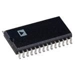
ICGOO电子元器件商城为您提供AD5544ARSZ由Analog设计生产,在icgoo商城现货销售,并且可以通过原厂、代理商等渠道进行代购。 AD5544ARSZ价格参考。AnalogAD5544ARSZ封装/规格:数据采集 - 数模转换器, 16 位 数模转换器 4 28-SSOP。您可以下载AD5544ARSZ参考资料、Datasheet数据手册功能说明书,资料中有AD5544ARSZ 详细功能的应用电路图电压和使用方法及教程。
AD5544ARSZ 是由 Analog Devices Inc.(亚德诺半导体公司)生产的一款高性能 16 位数模转换器(DAC),属于数据采集系统中的关键组件。其应用场景主要包括以下几个方面:

 1. 工业自动化与过程控制
AD5544ARSZ 可用于工业自动化领域,例如 PLC(可编程逻辑控制器)、DCS(分布式控制系统)和 SCADA(监控与数据采集系统)。它能够将数字信号转换为高精度的模拟信号,用于控制阀门、电机或其他执行机构的速度、位置或压力等参数。

 2. 测试与测量设备
在精密测试仪器中,如示波器、信号发生器和电源供应器,AD5544ARSZ 提供了高分辨率和低噪声的输出能力。这使得它可以生成精确的电压波形,满足实验室和生产环境中的严格要求。

 3. 通信系统
该 DAC 可应用于无线通信基站、卫星通信以及光纤通信系统中。通过将数字基带信号转换为模拟射频信号,支持复杂的调制解调功能,从而实现高质量的数据传输。

 4. 医疗设备
在医疗成像设备(如超声波机、CT 扫描仪)和生命体征监测仪(如心电图仪)中,AD5544ARSZ 能够确保信号的高保真度和稳定性,这对于诊断结果的准确性至关重要。

 5. 音频处理
对于专业音频设备,例如数字混音台、录音棚设备和高保真音响系统,这款 DAC 的优异线性度和低失真特性使其成为理想选择,可以还原细腻的声音细节。

 6. 汽车电子
在现代汽车中,AD5544ARSZ 可用于车载娱乐系统、导航系统以及自动驾驶相关的传感器接口中,提供可靠的信号转换服务。

总之,AD5544ARSZ 凭借其卓越的性能指标(如低功耗、高精度和快速建立时间),适用于需要精准模拟信号输出的各种高端应用场合。
| 参数 | 数值 |
| 产品目录 | 集成电路 (IC)半导体 |
| 描述 | IC DAC 16BIT QUAD SRL IN 28-SSOP数模转换器- DAC PREC QUAD 16-Bit IC |
| 产品分类 | |
| 品牌 | Analog Devices |
| 产品手册 | |
| 产品图片 |
|
| rohs | 符合RoHS无铅 / 符合限制有害物质指令(RoHS)规范要求 |
| 产品系列 | 数据转换器IC,数模转换器- DAC,Analog Devices AD5544ARSZ- |
| 数据手册 | |
| 产品型号 | AD5544ARSZ |
| 产品培训模块 | http://www.digikey.cn/PTM/IndividualPTM.page?site=cn&lang=zhs&ptm=19145http://www.digikey.cn/PTM/IndividualPTM.page?site=cn&lang=zhs&ptm=18614http://www.digikey.cn/PTM/IndividualPTM.page?site=cn&lang=zhs&ptm=26125http://www.digikey.cn/PTM/IndividualPTM.page?site=cn&lang=zhs&ptm=26140http://www.digikey.cn/PTM/IndividualPTM.page?site=cn&lang=zhs&ptm=26150http://www.digikey.cn/PTM/IndividualPTM.page?site=cn&lang=zhs&ptm=26146http://www.digikey.cn/PTM/IndividualPTM.page?site=cn&lang=zhs&ptm=26147 |
| 产品目录页面 | |
| 产品种类 | 数模转换器- DAC |
| 位数 | 16 |
| 供应商器件封装 | 28-SSOP |
| 分辨率 | 16 bit |
| 包装 | 管件 |
| 商标 | Analog Devices |
| 安装类型 | 表面贴装 |
| 安装风格 | SMD/SMT |
| 封装 | Tube |
| 封装/外壳 | 28-SSOP(0.209",5.30mm 宽) |
| 封装/箱体 | SSOP-28 |
| 工作温度 | -40°C ~ 125°C |
| 工厂包装数量 | 47 |
| 建立时间 | 900ns |
| 接口类型 | SPI |
| 数据接口 | SPI |
| 最大功率耗散 | 1.25 mW |
| 最大工作温度 | + 125 C |
| 最小工作温度 | - 40 C |
| 标准包装 | 1 |
| 电压参考 | External |
| 电压源 | 双 ± |
| 电源电压-最大 | 5.5 V |
| 电源电压-最小 | 2.7 V |
| 积分非线性 | +/- 2 LSB |
| 稳定时间 | 0.9 us |
| 系列 | AD5544 |
| 结构 | R-2R |
| 转换器数 | 4 |
| 转换器数量 | 4 |
| 输出数和类型 | 4 电流,单极4 电流,双极 |
| 输出类型 | Current |
| 配用 | /product-detail/zh/EV-AD5544%2F45SDZ/EV-AD5544%2F45SDZ-ND/4866743 |
| 采样比 | 500 kSPs |
| 采样率(每秒) | - |


- 商务部:美国ITC正式对集成电路等产品启动337调查
- 曝三星4nm工艺存在良率问题 高通将骁龙8 Gen1或转产台积电
- 太阳诱电将投资9.5亿元在常州建新厂生产MLCC 预计2023年完工
- 英特尔发布欧洲新工厂建设计划 深化IDM 2.0 战略
- 台积电先进制程称霸业界 有大客户加持明年业绩稳了
- 达到5530亿美元!SIA预计今年全球半导体销售额将创下新高
- 英特尔拟将自动驾驶子公司Mobileye上市 估值或超500亿美元
- 三星加码芯片和SET,合并消费电子和移动部门,撤换高东真等 CEO
- 三星电子宣布重大人事变动 还合并消费电子和移动部门
- 海关总署:前11个月进口集成电路产品价值2.52万亿元 增长14.8%


PDF Datasheet 数据手册内容提取
Quad, Current-Output, Serial-Input 16-/14-Bit DACs Data Sheet AD5544/AD5554 FEATURES FUNCTIONAL BLOCK DIAGRAM AD5544: 16-bit resolution VAREFVBREFVCREFVDREF INL of ±1 LSB (B Grade) 16-BIT (AD5544) AD5554: 14-bit resolution D0 14-BIT (AD5554) VDD 2 mINAL f oufl l±-s0c.a5l eL ScBu r(rBe Gntr a±d 2e0) %, with VREF = ±10 V SDO DDDD1234 REINGPISUTTER R REDGAICST AER R DAC A IROFUBTAA 0.9 μs settling time to ±0.1% D5 AGNDA D6 12 MHz multiplying bandwidth DD78 RFBB Midscale glitch of −1 nV-sec DD190 REINGPISUTTER R REDGAICS TBER R DAC B IOUTB Midscale or zero-scale reset DD1112 AGNDB D13 4 separate, 4-quadrant multiplying reference inputs D14 RFBC SPI-compatible, 3-wire interface SDI DAA1015 REINGPISUTTER R REDGAICS TCER R DAC C IOUTC Double-buffered registers enable AGNDC CS Simultaneous multichannel change CLK EN RFBD Internal power-on reset DACA REINGPISUTTER R REDGAICS TDER R DAC D IOUTD Temperature range: −40°C to +125°C B AGNDD C Compact 28-lead SSOP and 32-lead LFCSP 2:4 D DECODE PORWEESRE-TON AGNDF AD5544/AD55541 AAuPtPomLIaCtiAcT teIOst NeqSu ipment DGND RS MSB LDAC VSS 00943-001 Instrumentation 1AD5544 IS 16-BIT;AD5554 IS 14-BIT Figure 1. Digitally controlled calibration GENERAL DESCRIPTION The AD5544/AD5554 quad, 16-/14-bit, current output, digital- The AD5544 is packaged in the compact 28-lead SSOP and 32-lead to-analog converters (DACs) are designed to operate from a LFCSP. The AD5554 is packaged in the compact 28-lead SSOP. 2.7 V to 5.5 V supply range. The EV-AD5544/45SDZ is available for evaluating DAC perfor- The applied external reference input voltage (V x) determines mance. For more information, see the UG-285 evaluation board REF the full-scale output current. Integrated feedback resistors (R ) user guide. FB provide temperature-tracking, full-scale voltage outputs when 0.7 combined with an external I-to-V precision amplifier. 0.6 A double-buffered serial data interface offers high speed, 3-wire, 0.5 SPI- and microcontroller-compatible inputs using serial data in (SDI), a chip select (CS), and clock (CLK) signals. In addition, B) 0.4 S a serial data out pin (SDO) allows for daisy-chaining when multiple R (L 0.3 O packages are used. A common, level-sensitive, load DAC strobe R R 0.2 (LDAC) input allows the simultaneous update of all DAC outputs L E from previously loaded input registers. Additionally, an internal IN 0.1 power-on reset forces the output voltage to 0 at system turn-on. 0 tToh zee MroS cBo pdien w ahlloenw sM sySsBt e=m 0 r oesre tto a hssaelrf-tisocnal (eR cSo)d teo wfohrecne aMll SrBeg =is t1e.r s ––00..12 00943-002 0 10,000 20,000 30,000 40,000 50,000 60,000 70,000 CODE Figure 2. AD5544 INL vs. Code Plot (TA = 25°C) Rev. H Document Feedback Information furnished by Analog Devices is believed to be accurate and reliable. However, no responsibility is assumed by Analog Devices for its use, nor for any infringements of patents or other One Technology Way, P.O. Box 9106, Norwood, MA 02062-9106, U.S.A. rights of third parties that may result from its use. Specifications subject to change without notice. No license is granted by implication or otherwise under any patent or patent rights of Analog Devices. Tel: 781.329.4700 ©2000–2015 Analog Devices, Inc. All rights reserved. Trademarks and registered trademarks are the property of their respective owners. Technical Support www.analog.com
AD5544/AD5554 Data Sheet TABLE OF CONTENTS Features .............................................................................................. 1 Digital-to-Analog Converter (DAC) ....................................... 14 Applications ....................................................................................... 1 Serial Data Interface ....................................................................... 16 Functional Block Diagram .............................................................. 1 Truth Tables................................................................................. 17 General Description ......................................................................... 1 Power-On Reset .......................................................................... 18 Revision History ............................................................................... 2 ESD Protection Circuits ............................................................ 18 Specifications ..................................................................................... 4 Power Supply Sequence ............................................................. 18 AD5544 Electrical Characteristics ............................................. 4 Layout and Power Supply Bypassing ....................................... 19 AD5554 Electrical Characteristics ............................................. 5 Grounding ................................................................................... 19 Timing Diagrams .......................................................................... 7 Applications Information .............................................................. 20 Absolute Maximum Ratings ............................................................ 8 Reference Selection .................................................................... 20 ESD Caution .................................................................................. 8 Amplifier Selection .................................................................... 20 Pin Configurations and Function Descriptions ........................... 9 Outline Dimensions ....................................................................... 22 Typical Performance Characteristics ........................................... 11 Ordering Guide .......................................................................... 23 Theory of Operation ...................................................................... 14 REVISION HISTORY 9/15—Rev. G to Rev. H Changed NC to DNC .................................................... Throughout 9/09—Rev. C to Rev. D Changes to Figure 1 .......................................................................... 1 Changes to Features Section ............................................................ 1 Changes to Figure 6 and Table 4 ..................................................... 9 Changes to Table 1 ............................................................................. 3 Changes to Table 2 ............................................................................. 4 5/13—Rev. F to Rev. G Changes to Figure 12 ......................................................................... 9 Changes to General Description Section ...................................... 1 Changes to Figure 19 ...................................................................... 10 Deleted Evaluation Board for the AD5544 Section and Changes to Table 8 and Table 9 .................................................... 13 Figure 30 to Figure 35; Renumbered Sequentially ..................... 22 Changes to Ordering Guide .......................................................... 16 Updated Outline Dimensions ....................................................... 21 Changes to Ordering Guide .......................................................... 22 8/09—Rev. B to Rev. C Change to Table 1 .............................................................................. 3 1/12—Rev. E to Rev. F Change to Table 2 .............................................................................. 4 Changes to Figure 1 .......................................................................... 1 Added Figure 18; Renumbered Sequentially .............................. 11 8/09—Rev. A to Rev. B Changes to Evaluation Board Schematics Section ..................... 22 Changes to Features Section ............................................................ 1 Changes to Figure 2 ........................................................................... 1 6/11—Rev. D to Rev. E Changes to Table 1 ............................................................................. 3 Added 32-Lead LFCSP .................................................. Throughout Changes to Table 2 ............................................................................. 4 Changes to Table 1, Supply Characteristics Parameters .............. 3 Moved Timing Diagram ................................................................... 5 Changes to Table 2, Supply Characteristics Parameters .............. 5 Added Figure 4; Renumbered Sequentially ................................... 5 Added Figure 6, Renumbered Subsequent Figures, Changes Change to Table 3 .............................................................................. 6 to Table 4 ............................................................................................ 7 Changes to Table 4 ............................................................................. 7 Changed Applications Section to Applications Information Changes to Typical Performance Characteristics Section ........... 8 Section, Added Reference Selection and Amplifier Selection Changes to Figure 19 ...................................................................... 10 Sections ............................................................................................ 19 Moved Table 5, Table 6, and Table 7 ............................................ 12 Added Evaluation Board for the AD5544 Section ..................... 21 Moved Truth Tables Section ......................................................... 13 Updated Outline Dimensions ....................................................... 17 Deleted Figure 27; Renumbered Sequentially ............................ 14 Changes to Ordering Guide .......................................................... 18 Updated Outline Dimensions ....................................................... 16 Changes to Ordering Guide .......................................................... 16 Rev. H | Page 2 of 24
Data Sheet AD5544/AD5554 12/04—Rev. 0 to Rev. A Addition of Layout and Power Supply Bypassing Section ......... 19 Updated Format.................................................................. Universal Addition of Grounding Section .................................................... 19 Change to Electrical Characteristics Tables ................................... 4 Addition of Figure 32 ...................................................................... 19 Change to Pin Description Table .................................................. 10 Addition of Power Supply Sequence Section ............................... 19 4/00—Revision 0: Initial Version Rev. H | Page 3 of 24
AD5544/AD5554 Data Sheet SPECIFICATIONS AD5544 ELECTRICAL CHARACTERISTICS V = 2.7 V to 5.5 V, V = 0 V, I x = virtual GND, A x = 0 V, V A = V B = V C = V D = 10 V, T = full operating temperature DD SS OUT GND REF REF REF REF A range of −40°C to +125°C, unless otherwise noted. Table 1. Parameter Symbol Test Condition/Comments Min Typ Max Unit STATIC PERFORMANCE1 Resolution N 1 LSB = V x/216 = 153 µV when V = 10 V 16 Bits REF REF Relative Accuracy INL AD5544BRSZ ±1 LSB AD5544ARSZ ±2 LSB AD5544BCPZ ±1 LSB AD5544ACPZ-1 ±4 LSB Differential Nonlinearity DNL AD5544BRSZ ±1 LSB AD5544ARSZ ±1.5 LSB AD5544BCPZ ±1 LSB AD5544ACPZ-1 ±1 LSB Output Leakage Current I x Data = 0x0000, T = 25°C 10 nA OUT A Data = 0x0000, T = 85°C 20 nA A Full-Scale Gain Error G Data = 0xFFFF ±0.75 ±3 mV FSE Full-Scale Tempco2 TCV 1 ppm/°C FS Feedback Resistor R x V = 5 V 4 6 8 kΩ FB DD REFERENCE INPUT V x Range V x −15 +15 V REF REF Input Resistance R x 4 6 8 kΩ REF Input Resistance Match R x Channel-to-channel 0.35 % REF Input Capacitance2 C x 5 pF REF ANALOG OUTPUT Output Current I x Data = 0xFFFF 1.25 2.5 mA OUT Output Capacitance2 C x Code dependent 35 pF OUT LOGIC INPUT AND OUTPUT Logic Input Low Voltage V 0.8 V IL Logic Input High Voltage V 2.4 V IH Input Leakage Current I 1 µA IL Input Capacitance2 C 10 pF IL Logic Output Low Voltage V I = 1.6 mA 0.4 V OL OL Logic Output High Voltage V I = 100 µA 4 V OH OH INTERFACE TIMING2, 3 Clock Width High t 25 ns CH Clock Width Low t 25 ns CL CS to Clock Setup t 0 ns CSS Clock to CS Hold t 25 ns CSH Clock to SDO Propagation t 2 20 ns PD Delay Load DAC Pulse Width t 25 ns LDAC Data Setup t 20 ns DS Data Hold t 20 ns DH Load Setup t 5 ns LDS Load Hold t 25 ns LDH SUPPLY CHARACTERISTICS Power Supply Range V 2.7 5.5 V DD RANGE Positive Supply Current I Logic inputs = 0 V 5 µA DD Negative Supply Current I Logic inputs = 0 V, V = −5 V 0.001 9 µA SS SS Rev. H | Page 4 of 24
Data Sheet AD5544/AD5554 Parameter Symbol Test Condition/Comments Min Typ Max Unit Power Dissipation P Logic inputs = 0 V 1.25 mW DISS Power Supply Sensitivity PSS ∆V = ±5% 0.006 %/% DD AC CHARACTERISTICS4 Output Voltage Settling Time t To ±0.1% of full scale, data = 0x0000 to 0xFFFF to 0x0000 0.9 µs S Reference Multiplying BW − 3 dB V x = 5 V p-p, data = 0xFFFF, C = 2.0 pF, 12 MHz REF FB Bandwidth (BW) DAC Glitch Impulse Q V x = 8 V, data = 0x0000 to 0x8000 to 0x0000 −1 nV-sec REF Feedthrough Error V x/V x Data = 0x0000, V x = 100 mV rms, f = 100 kHz −65 dB OUT REF REF Crosstalk Error V A/V B Data = 0x0000, V B = 100 mV rms, adjacent channel, −90 dB OUT REF REF f = 100 kHz Digital Feedthrough Q CS = 1, f = 1 MHz 0.6 nV-sec CLK Total Harmonic Distortion THD V x = 5 V p-p, data = 0xFFFF, f = 1 kHz −98 dB REF Output Spot Noise Voltage e f = 1 kHz, BW = 1 Hz 7 nV/√Hz N 1 All static performance tests (except I x) are performed in a closed-loop system using an external precision OP177 I-to-V converter amplifier. The AD5544 R terminal OUT FB is tied to the amplifier output. Typical values represent average readings measured at 25°C. 2 These parameters are guaranteed by design and not subject to production testing. 3 All input control signals are specified with t = t = 2.5 ns (10% to 90% of 3 V) and timed from a voltage level of 1.5 V. R F 4 All ac characteristic tests are performed in a closed-loop system using an AD8038 I-to-V converter amplifier. AD5554 ELECTRICAL CHARACTERISTICS V = 2.7 V to 5.5 V, V = 0 V, I x = virtual GND, A x = 0 V, V A = V B = V C = V D = 10 V, T = full operating temperature DD SS OUT GND REF REF REF REF A range of −40°C to +125°C, unless otherwise noted. Table 2. Parameter Symbol Test Condition/Comments Min Typ Max Unit STATIC PERFORMANCE1 Resolution N 1 LSB = V x/214 = 610 µV when V x = 10 V 14 Bits REF REF Relative Accuracy INL ±0.5 LSB Differential Nonlinearity DNL ±1 LSB Output Leakage Current I x Data = 0x0000, T = 25°C 10 nA OUT A Data = 0x0000, T = 85°C 20 nA A Full-Scale Gain Error G Data = 0x3FFF ±2 ±10 mV FSE Full-Scale Tempco2 TCV 1 ppm/°C FS Feedback Resistor R x V = 5 V 4 6 8 kΩ FB DD REFERENCE INPUT V x Range V x −15 +15 V REF REF Input Resistance R x 4 6 8 kΩ REF Input Resistance Match R x Channel-to-channel 1 % REF Input Capacitance2 C x 5 pF REF ANALOG OUTPUT Output Current I x Data = 0x3FFF 1.25 2.5 mA OUT Output Capacitance2 C x Code dependent 80 pF OUT LOGIC INPUT AND OUTPUT Logic Input Low Voltage V 0.8 V IL Logic Input High Voltage V 2.4 V IH Input Leakage Current I 1 µA IL Input Capacitance2 C 10 pF IL Logic Output Low Voltage V I = 1.6 mA 0.4 V OL OL Logic Output High Voltage V I = 100 µA 4 V OH OH INTERFACE TIMING2, 3 Clock Width High t 25 ns CH Clock Width Low t 25 ns CL CS to Clock Setup t 0 ns CSS Rev. H | Page 5 of 24
AD5544/AD5554 Data Sheet Parameter Symbol Test Condition/Comments Min Typ Max Unit Clock to CS Hold t 25 ns CSH Clock to SDO Propagation t 2 20 ns PD Delay Load DAC Pulse Width t 25 ns LDAC Data Setup t 20 ns DS Data Hold t 20 ns DH Load Setup t 5 ns LDS Load Hold t 25 ns LDH SUPPLY CHARACTERISTICS Power Supply Range V 2.7 5.5 V DD RANGE Positive Supply Current I Logic inputs = 0 V 5 µA DD Negative Supply Current I Logic inputs = 0 V, V = −5 V 0.001 9 µA SS SS Power Dissipation P Logic inputs = 0 V 1.25 mW DISS Power Supply Sensitivity PSS ∆V = ±5% 0.006 %/% DD AC CHARACTERISTICS4 Output Voltage Settling Time t To ±0.1% of full scale, data = 0x0000 to 0x3FFF to 0x0000 0.9 µs S Reference Multiplying BW − 3 dB V x = 5 V p-p, data = 0xFFFF, C = 2.0 pF 12 MHz REF FB Bandwidth (BW) DAC Glitch Impulse Q V x = 8 V, data = 0x0000 to 0x2000 to 0x0000 −1 nV-sec REF Feedthrough Error V x/V x Data = 0x0000, V x = 100 mV rms, f = 100 kHz −65 dB OUT REF REF Crosstalk Error V A/V B Data = 0x0000, V B = 100 mV rms, adjacent channel, −90 dB OUT REF REF f = 100 kHz Digital Feedthrough Q CS = 1, f = 1 MHz 0.6 nV-sec CLK Total Harmonic Distortion THD V x = 5 V p-p, data = 0x3FFF, f = 1 kHz −98 dB REF Output Spot Noise Voltage e f = 1 kHz, BW = 1 Hz 7 nV/√Hz N 1 All static performance tests (except I ) are performed in a closed-loop system using an external precision OP177 I-to-V converter amplifier. The AD5554 R terminal is OUT FB tied to the amplifier output. Typical values represent average readings measured at 25°C. 2 These parameters are guaranteed by design and not subject to production testing. 3 All input control signals are specified with t = t = 2.5 ns (10% to 90% of 3 V) and timed from a voltage level of 1.5 V. R F 4 All ac characteristic tests are performed in a closed-loop system using an AD8038 I-to-V converter amplifier,. Rev. H | Page 6 of 24
Data Sheet AD5544/AD5554 TIMING DIAGRAMS SDI A1 A0 D15 D14 D13 D12 D11 D10 D1 D0 INPUT CLK REG LD CS tCSS tDS tDH tCH tCL tCSH LDAC tLDS tLDH tPD tLDAC SDO 00943-004 Figure 3. AD5544 Timing Diagram SDI A1 A0 D13 D12 D11 D10 D09 D08 D1 D0 INPUT CLK REG LD CS tCSS tDS tDH tCH tCL tCSH LDAC tLDS tLDH tPD tLDAC SDO 00943-005 Figure 4. AD5554 Timing Diagram Rev. H | Page 7 of 24
AD5544/AD5554 Data Sheet ABSOLUTE MAXIMUM RATINGS Stresses at or above those listed under Absolute Maximum Table 3. Ratings may cause permanent damage to the product. This is a Parameter Rating stress rating only; functional operation of the product at these V to GND −0.3 V, +8 V DD or any other conditions above those indicated in the operational V to GND +0.3 V, −7 V SS section of this specification is not implied. Operation beyond V x to GND −18 V, +18 V REF the maximum operating conditions for extended periods may Logic Input and Output to GND −0.3 V, +8 V affect product reliability. V(I x) to GND −0.3 V, V + 0.3 V OUT DD A x to DGND −0.3 V, +0.3 V GND Input Current to Any Pin Except Supplies ±50 mA ESD CAUTION Package Power Dissipation (TJ max − TA)/θJA Thermal Resistance θJA 28-Lead SSOP 100°C/W 32-Lead LFCSP 32.5°C/W Maximum Junction Temperature (T Max) 150°C J Operating Temperature Range −40°C to +125°C Storage Temperature Range −65°C to +150°C Lead Temperature Vapor Phase, 60 Sec 215°C Infrared, 15 Sec 220°C Rev. H | Page 8 of 24
Data Sheet AD5544/AD5554 PIN CONFIGURATIONS AND FUNCTION DESCRIPTIONS AIGONUDTAA 12 2287 AIOGUNTDDD 32VAREF31DNCIA30OUTAA29GND28ADGND27IDOUT26DNCDNC25 VREFA 3 26 VREFD RFBA 4 25 RFBD RFBA 1 24 VREFD MSB 5 24 DGND MSRBS 23 2232 RDGFBNDD VRDSD 67 AADD55554544/ 2232 VASGSNDF CVCLDKSD 456 (NAToOtD Pto5 V 5SIE4cWa4le) 221109 VALDSGSANDCF CS 8 TOP VIEW 21 LDAC SDI 7 18 SDO CLK 9 (Not to Scale) 20 SDO RFBB 8 17 RFBC SDI 10 19 DNC 910111213141516 VRRFEBFBB 1112 1187 RVRFBEFCC DNCVBREFIBOUTABGNDACGNDICOUTVCREFDNC IOUTB 13 16 IOUTC NOTES DNC = DO NAOGTN CDOBN1N4ECT. LEAVE THE1 5PIANG UNNDCCONNECTED. 00943-003 1 2 .. DCLENOACNV N=EE DTCOHT E NT OPHIETN C EUXONPNCONOSENECNDTE.PCATDEDT.OAGNDx. 00943-035 Figure 5. TSSOP Pin Configuration Figure 6. LFCSP Pin Configuration Table 4. Pin Function Descriptions TSSOP LFCSP Pin No. Pin No. Mnemonic Description 1 29 A A DAC A Analog Ground. GND 2 30 I A DAC A Current Output. OUT 3 32 V A DAC A Reference Voltage Input Terminal. Establishes DAC A full-scale output voltage. This pin can REF be tied to the V pin. DD 4 1 R A DAC A Feedback Resistor Connection. Establish the voltage output for DAC A by connecting this pin FB to an external amplifier output. 5 2 MSB MSB Bit. Set this pin during a reset pulse (RS) or at system power-on if tied to ground or V . DD 6 3 RS Reset Pin, Active Low Input. Input registers and DAC registers are set to all 0s or half-scale code (0x8000 for the AD5544 and 0x2000 for the AD5554), determined by the voltage on the MSB pin. Register data = 0x0000 when MSB = 0. 7 4 VDD Positive Power Supply Input. Specified range of operation: 5 V ± 10%. 8 5 CS Chip Select, Active Low Input. Disables shift register loading when high. Transfers serial register data to the input register when CS/LDAC returns high. Does not affect LDAC operation. 9 6 CLK Clock Input. Positive edge clocks data into the shift register. 10 7 SDI Serial Data Input. Input data loads directly into the shift register. 11 8 R B DAC B Feedback Resistor Connection. Establish the voltage output for DAC B by connecting this pin FB to an external amplifier output. 12 10 V B DAC B Reference Voltage Input Terminal. Establishes DAC B full-scale output voltage. This pin can be REF tied to the V pin. DD 13 11 I B DAC B Current Output. OUT 14 12 A B DAC B Analog Ground. GND 15 13 A C DAC C Analog Ground. GND 16 14 I C DAC C Current Output. OUT 17 15 V C DAC C Reference Voltage Input Terminal. Establishes DAC C full-scale output voltage. This pin can REF be tied to the V pin. DD 18 17 R C DAC C Feedback Resistor Connection. Establish the voltage output for DAC C by connecting this pin FB to an external amplifier output. 19 9, 16, 25, DNC Do Not Connect. Leave these pins unconnected. 26, 31 20 18 SDO Serial Data Output. Input data loads directly into the shift register. Data appears at SDO at 19 clock pulses for the AD5544 and 17 clock pulses for the AD5554 after input at the SDI pin. 21 19 LDAC Load DAC Register Strobe, Level Sensitive Active Low. Transfers all input register data to DAC registers. Asynchronous active low input. See Table 8 and Table 9 for operation. Rev. H | Page 9 of 24
AD5544/AD5554 Data Sheet TSSOP LFCSP Pin No. Pin No. Mnemonic Description 22 20 A F High Current Analog Force Ground. GND 23 21 VSS Negative Bias Power Supply Input. Specified range of operation: −5.5 V to +0.3 V. 24 22 DGND Digital Ground Pin. 25 23 R D DAC D Feedback Resistor Connection. Establish the voltage output for DAC D by connecting this FB pin to an external amplifier output. 26 24 V D DAC D Reference Voltage Input Terminal. Establishes DAC D full-scale output voltage. This pin can REF be tied to the V pin. DD 27 27 I D DAC D Current Output. OUT 28 28 A D DAC D Analog Ground. GND N/A1 EPAD Connect the exposed pad to AGNDx. 1 N/A means not applicable. Rev. H | Page 10 of 24
Data Sheet AD5544/AD5554 TYPICAL PERFORMANCE CHARACTERISTICS 0.10 1.5 0x0FFF VDD = 5V 0.05 VREF = 10V 1.0 0 0xF000 –0.05 B) 0.5 S RROR (L ––00..1105 L (LSB) 0 0x7FFF 0x8000 E N L –0.20 I N D –0.5 –0.25 –0.30 –1.0 ––00..34500 10,000 20,000 30,00C0OD4E0,000 50,000 60,000 70,0000943-0060 –1–.52000 –1500 –1000 OF–5F0S0ET VO0LTAGE50 (0µV) 1000 1500 200000943-009 Figure 7. AD5544 DNL vs. Code, T = 25°C Figure 10. AD5544 Integral Nonlinearity Error vs. Op Amp Offset A 0.20 1.00 VDD = 5V 0.15 0.75 VREF = 10V 0.10 0.50 B) S 0.05 0.25 R (L SB) 0x0FFF NL ERRO –0.050 DNL (L–0.250 0xF000 I 0x8000 –0.10 –0.50 ––00..12500 2000 4000 6000 800C0O1D0E,00012,00014,00016,00018,0000943-0070 ––10..07–051000 –750 –500 O–P25 A0MP O0FFSET2 (5µ0V) 500 750 100000943-011 Figure 8. AD5554 INL vs. Code, T = 25°C Figure 11. AD5544 Differential Nonlinearity Error vs. Op Amp Offset A 0.10 10 VDD = 5V VREF = 10V 5 0.05 B) B) 0 S S R (L 0 R (L RO RO –5 R R E E L –0.05 N DN GAI –10 –0.10 –15 –0.150 2000 4000 6000 800C0O1D0E,00012,00014,00016,00018,0000943-0080 –2–01500 –1000 –5O00P AMP O0FFSET (µV50)0 1000 1500 00943-013 Figure 9. AD5554 DNL vs. Code, T = 25°C Figure 12. AD5544 Gain Error vs. Op Amp Offset A Rev. H | Page 11 of 24
AD5544/AD5554 Data Sheet –3.88 10,000 –3.90 –3.92 1000 ZERO SCALE –3.94 MIDSCALE FULL SCALE (V)OUT––33..9986 (µA)D 100 0x5555 V D –4.00 I –4.02 10 –4.04 –4.06 –4.080.4 0.5 0.6 0.7 TIM0E.8 (µs) 0.9 1.0 1.1 1.2 00943–012 11k 10k CLOC1K0 F0kREQUENC1YM (Hz) 10M 100M 00943-015 Figure 13. AD5544 Midscale Transition Figure 16. AD5544 Power Supply Current vs. Clock Frequency 100 VVDRDEF = = 5 1V0V 90 VVDRDEF = = 5 1V0V 80 VOUT 70 V B) 60 5V/DI LDAC RR (d 50 S P 40 30 20 00943-018 100 100 1k FREQU1E0NkCY (Hz) 100k 1M 00943-020 Figure 14. AD5544 Large Signal Settling Time Figure 17. AD5544/AD5554 Power Supply Rejection vs. Frequency 0.1 4 20 0 0 –20 B) 0 –4 M (d –40 U (V)UT –8 AC (V) ECTR –60 VO LD R SP –80 E –0.1 –12 W–100 O P –120 –16 –140 –0.2–2 0 2 TIME4 (µs) 6 8 10–20 00943-019 –1600 5k F1R0EkQUENCY (1H5zk) 20k 25k 00943-118 Figure 15. AD5544 Small Signal Settling Time Figure 18. AD5544/AD5554 Analog THD Rev. H | Page 12 of 24
Data Sheet AD5544/AD5554 300 250 A) T (µ 200 N E R UR 150 Y C L P UP 100 S 50 0 0 0.5 1.0 1.5 L2O.0GIC 2IN.5PUT3 (.V0) 3.5 4.0 4.5 5.0 00943-017 Figure 19. AD5544/AD5554 Power Supply Current vs. Logic Input Voltage Rev. H | Page 13 of 24
AD5544/AD5554 Data Sheet THEORY OF OPERATION The AD5544 and the AD5554 contain four 16-bit and 14-bit, These DACs are also designed to accommodate ac reference input current output DACs, respectively. Each DAC has its own inde- signals. Both the AD5544 and the AD5554 accommodate input pendent multiplying reference input. Both the AD5544 and the reference voltages in the range of −15 V to +15 V. The reference AD5554 use a 3-wire, SPI-compatible serial data interface, with voltage inputs exhibit a constant nominal input resistance of 5 kΩ ± a configurable asynchronous RS pin for half-scale (MSB = 1) or 30%. On the other hand, the I A, I B, I C, and I D OUT OUT OUT OUT zero-scale (MSB = 0) preset. In addition, an LDAC strobe enables DAC outputs are code dependent and produce various output 4-channel, simultaneous updates for hardware synchronized resistances and capacitances. The choice of external amplifier output voltage changes. should take into account the variation in impedance generated by the AD5544/AD5554 on the inverting input node of the amplifier. DIGITAL-TO-ANALOG CONVERTER (DAC) The feedback resistance, in parallel with the DAC ladder resistance, Each part contains four current-steering R-R ladder DACs. dominates output voltage noise. For multiplying mode applications, Figure 20 shows a typical equivalent DAC. Each DAC contains an external feedback compensation capacitor, C , may be needed FB a matching feedback resistor for use with an external I-to-V to provide a critically damped output response for step changes in converter amplifier. The RFBx pin connects to the output of the reference input voltages. Figure 21 shows the gain vs. frequency external amplifier. The I x terminal connects to the inverting performance at various attenuation settings using a 23 pF external OUT input of the external amplifier. The A x pin should be Kelvin- feedback capacitor connected across the I x and R x terminals GND OUT FB connected to the load point, requiring full 16-bit accuracy. These for the AD5544 and the AD5554, respectively. To maintain good DACs are designed to operate with both negative and positive analog performance, power supply bypassing of 0.01 µF, in parallel reference voltage. with 1 µF, is recommended. Under these conditions, a clean power The V power pin is used only by the logic to drive the DAC supply with low ripple voltage capability should be used. Switching DD switches on and off. Note that a matching switch is used in power supplies is usually not suitable for this application due to series with the internal 5 kΩ feedback resistor. If users attempt the higher ripple voltage and PSS frequency-dependent characteris- to measure the value of R , power must be applied to V to tics. It is best to derive the supply of the AD5544/AD5554 from FB DD achieve continuity. An additional V bias pin is used to guard the system analog supply voltages. Do not use the digital supply SS substrate during high temperature applications, minimizing zero- (see Figure 22). scale leakage currents that double every 10°C. The DAC output 2 voltage is determined by V and the digital data (D) in the REF following equations: 0 D V =−V × (for the AD5544) (1) OUT REF 65,536 B) –2 d VOUT =−VREF ×16,D384 (for the AD5554) (2) GAIN ( –4 Note that the output polarity is opposite the V polarity for dc REF reference voltages. –6 VDD R R R VREFX 2R 2R 2R R 5kΩ RFBX –1800k 1MFREQUENCY (Hz)10M 100M 00943-026 Figure 21. AD5554 Reference Multiplying Bandwidth vs. Code S2 S1 IOUTX AGNDF AGNDX FROM OTHER DACSAGND VSS DGND DSWIGIITTCAHL EINST SE1RAFNADC ES 2COANRNE ECCLTOIOSENDS, OAMNIDT TVEDDD MFOURS TC BLAER PIOTYW.ERED. 00943-025 Figure 20. Typical Equivalent DAC Channel Rev. H | Page 14 of 24
Data Sheet AD5544/AD5554 15V ANALOG 2R POWER + 5V SUPPLY R VDD AD5544 RR R RFBX VREFX 2R 2R 2R R 5kΩ 15V S2 S1 IOUTX VCC AGNDF A1 VOUT AGNDX + VEE FROM OTHER DACSAGND LOAD VSS DGND DIGITAL INTERFACE CONNECTIONS OMITTED. FAONDR VCDLDA RMIUTYS TS WBEIT PCOHWESE RSE1DA.ND S2ARE CLOSED, 00943-028 Figure 22. Recommended Kelvin-Sensed Hookup Rev. H | Page 15 of 24
AD5544/AD5554 Data Sheet SERIAL DATA INTERFACE The AD5544/AD5554 use a 3-wire (CS, SDI, CLK), SPI-compatible Similarly, two right justified data bytes can be written to the serial data interface. Serial data of the AD5544/AD5554 is clocked AD5554. Keeping the CS line low between the first and second into the serial input register in an 18-bit and 16-bit data-word byte transfer results in a successful serial register update. format, respectively. The MSB bits are loaded first. Table 5 defines When the data is properly aligned in the shift register, the posi- the 18 data-word bits for the AD5544, and Table 6 defines the tive edge of the CS initiates the transfer of new data to the target 16 data-word bits for the AD5554. Data is placed on the SDI pin DAC register, determined by the decoding of Address Bit A1 and clocked into the register on the positive clock edge of CLK, and Address Bit A0. For the AD5544, Table 5, Table 7, Table 8, subject to the data setup and data hold time requirements specified and Figure 3 define the characteristics of the software serial in the interface timing specifications (see Table 1 and Table 2). interface. Data can be clocked in only while the CS chip select pin is active For the AD5554, Table 6, Table 7, Table 9, and Figure 4 define low. For the AD5544, only the last 18 bits clocked into the serial the characteristics of the software serial interface. Figure 23 and register are interrogated when the CS pin returns to the logic high Figure 24 show the equivalent logic interface for the key digital state; extra data bits are ignored. For the AD5554, only the last control pins for the AD5544. The AD5554 has a similar configura- 16 bits clocked into the serial register are interrogated when the tion, except that it has 14 data bits. Two additional pins, RS and CS pin returns to the logic high state. Because most microcontrol- MSB, provide hardware control over the preset function and lers output serial data in 8-bit bytes, three right justified data bytes DAC register loading. If these functions are not needed, the RS can be written to the AD5544. Keeping the CS line low between pin can be tied to logic high. The asynchronous input RS pin the first, second, and third byte transfers results in a successful forces all input and the DAC registers to either the zero-code serial register update. state (MSB = 0) or the half-scale state (MSB = 1). Table 5. AD5544 Serial Input Register Data Format (Data Is Loaded in the MSB-First Format)1 MSB LSB B17 B16 B15 B14 B13 B12 B11 B10 B9 B8 B7 B6 B5 B4 B3 B2 B1 B0 A1 A0 D15 D14 D13 D12 D11 D10 D9 D8 D7 D6 D5 D4 D3 D2 D1 D0 1 Only the last 18 bits of data clocked into the serial register (address + data) are inspected when the positive edge of the CS line returns to logic high. At this point, an internally generated load strobe transfers the serial register data contents (Bit D15 to Bit D0) to the decoded DAC input register address determined by Bit A1 and Bit A0. Any extra bits clocked into the AD5544 shift register are ignored; only the last 18 bits clocked in are used. If double-buffered data is not needed, the LDAC pin can be tied logic low to disable the DAC registers. Table 6. AD5554 Serial Input Register Data Format (Data Is Loaded in the MSB-First Format)1 MSB LSB B15 B14 B13 B12 B11 B10 B9 B8 B7 B6 B5 B4 B3 B2 B1 B0 A1 A0 D13 D12 D11 D10 D9 D8 D7 D6 D5 D4 D3 D2 D1 D0 1 Only the last 16 bits of data clocked into the serial register (address + data) are inspected when the positive edge of the CS line returns to logic high. At this point, an internally generated load strobe transfers the serial register data contents (Bit D13 to Bit D0) to the decoded DAC input register address determined by Bit A1 and Bit A0. Any extra bits clocked into the AD5554 shift register are ignored; only the last 16 bits clocked in are used. If double-buffered data is not needed, the LDAC pin can be tied logic low to disable the DAC registers. Table 7. Address Decode A1 A0 DAC Decoded 0 0 DAC A 0 1 DAC B 1 0 DAC C 1 1 DAC D Rev. H | Page 16 of 24
Data Sheet AD5544/AD5554 TRUTH TABLES Table 8. AD55441 Control Logic Truth Table CS CLK LDAC RS MSB2 Serial Shift Register Function3 Input Register Function DAC Register High X High High X No effect Latched Latched Low Low High High X No effect Latched Latched Low ↑ +3 High High X Shift register data advanced one bit Latched Latched Low High High High X No effect Latched Latched ↑ +3 Low High High X No effect Selected DAC updated with Latched current shift register contents4 High X Low High X No effect Latched Transparent High X High High X No effect Latched Latched High X ↑ +3 High X No effect Latched Latched High X High Low 0 No effect Latched data = 0x0000 Latched data = 0x0000 High X High Low High No effect Latched data = 0x8000 Latched data = 0x8000 1 For the AD5544, data appears at the SDO pin 19 clock pulses after input at the SDI pin. 2 X means don’t care. 3 ↑ + is a positive logic transition . 4 At power-on, both the input register and the DAC register are loaded with all 0s. Table 9. AD55541 Control Logic Truth Table CS CLK LDAC RS MSB2 Serial Shift Register Function3 Input Register Function3 DAC Register High X High High X No effect Latched Latched Low L High High X No effect Latched Latched Low ↑ +3 High High X Shift register data advanced one bit Latched Latched Low High High High X No effect Latched Latched ↑ +3 Low High High X No effect Selected DAC updated with current Latched shift register contents4 High X Low High X No effect Latched Transparent High X High High X No effect Latched Latched High X ↑ +3 High X No effect Latched Latched High X High Low 0 No effect Latched data = 0x0000 Latched data = 0x0000 High X High Low High No effect Latched data = 0x2000 Latched data = 0x2000 1 For the AD5554, data appears at the SDO pin 17 clock pulses after input at the SDI pin. 2 X means don’t care. 3 ↑ + is a positive logic transition . 4 At power-on, both the input register and the DAC register are loaded with all 0s. Rev. H | Page 17 of 24
AD5544/AD5554 Data Sheet VREFA B C D CS EN AD5544 VDD CLK SDI D0 16 RFBA DD12 REIGNPISUTTER R REDGAICSTAER R DACA IOUTA D3 AGNDA D4 D5 D6 D7 D8 D9 D10 RFBB D11 INPUT DACB DD1123 REGISTER R REGISTER R DACB IOUTB SDO DD1145 DACBA AGNDB A0 C A1 D 2:4 DECODE RFBC INPUT DACC REGISTER R REGISTER R DACC IOUTC AGNDC RFBD INPUT DACD REGISTER R REGISTER R DACD IOUTD AGNDD SET SET MSB MSB POWER- AGNDF ON RESET DGND MSB LDAC RS VSS 00943-029 Figure 23. System Level Digital Interfacing TO INPUT REGISTER ESD PROTECTION CIRCUITS A ADDRESS B All logic input pins contain back-biased ESD protection Zener CS DECODER C D diodes that are connected to ground (DGND) and VDD, as shown in Figure 25. EN CLK SHIFT REGISTER VDD SDI 19TH/17TH DIGITAL 5kΩ SDOFigure 24. AD5544/AD5554 Equivalent Logic InCtLeOrfCaKce 00943-030 INPUTS DGND 00943-031 POWER-ON RESET Figure 25. Equivalent ESD Production Circuits When the V power supply is turned on, an internal reset strobe POWER SUPPLY SEQUENCE DD forces all the input and DAC registers to the zero-code state or As standard practice, it is recommended that V , V , and ground DD SS half-scale state, depending on the MSB pin voltage. The V power DD be powered up prior to any reference. The ideal power-up sequence supply should have a smooth positive ramp without drooping to is as follows: A x, DGND, V , V , V x, and the digital inputs. GND DD SS REF have consistent results, especially in the region of V = 1.5 V to DD A noncompliance power-up sequence may elevate the reference 2.3 V. The V supply has no effect on the power-on reset perform- SS current, but the devices resume normal operation once V and DD ance. The DAC register data stays at a zero-scale or half-scale V are powered up. SS setting until a valid serial register data load takes place. Rev. H | Page 18 of 24
Data Sheet AD5544/AD5554 LAYOUT AND POWER SUPPLY BYPASSING AD5544/AD5554 It is good practice to employ a compact, minimum lead length VDD C3 + C1 VDD layout design. The leads to the input should be as direct as possible 10µF 0.1µF AGNDX with a minimum conductor length. Ground paths should have C4 C2 10µF 0.1µF low resistance and low inductance. VSS VSS DGND Sqiumaliiltayr clya,p iat ciist ogroso fodr p orpatcitmicuem to s tbaybpilaitsys. tShuep pployw leeard ssu tpop tlhiees d wevitihce 00943-032 Figure 26. Power Supply Bypassing and Grounding Connection should be bypassed with 0.01 μF to 0.1 μF disc or chip ceramic capacitors. Low ESR 1 μF to 10 μF tantalum or electrolytic capaci- GROUNDING tors should also be applied at V to minimize any transient DD The DGND and A x pins of the AD5544/AD5554 serve as GND disturbance and filter any low frequency ripple (see Figure 26). digital and analog ground references. To minimize the digital Users should not apply switching regulators for V due to the DD ground bounce, the DGND terminal should be joined remotely power supply rejection ratio (PSRR) degradation over frequency. at a single point to the analog ground plane (see Figure 26). Rev. H | Page 19 of 24
AD5544/AD5554 Data Sheet APPLICATIONS INFORMATION The AD5544/AD5554 are, inherently, two-quadrant multiplying REFERENCE SELECTION DACs. That is, they can be easily set up for unipolar output When selecting a reference for use with the AD55xx series operation. The full-scale output polarity is the inverse of the of current output DACs, pay attention to the output voltage, reference input voltage. temperature coefficient specification of the reference. Choosing In some applications, it may be necessary to generate the full a precision reference with a low output temperature coefficient four-quadrant multiplying capability or a bipolar output swing. minimizes error sources. Table 10 lists some of the references This is easily accomplished using an additional external ampli- available from Analog Devices, Inc., that are suitable for use fier (A2) configured as a summing amplifier (see Figure 27). with this range of current output DACs. 10kΩ AMPLIFIER SELECTION 10kΩ 10V The primary requirement for the current-steering mode is an 5kΩ VREF A2 VOUT amplifier with low input bias currents and low input offset voltage. AD588 –10V < VOUT < +10V Because of the code-dependent output resistance of the DAC, the input offset voltage of an op amp is multiplied by the variable VDD VREFX RFBX gain of the circuit. A change in this noise gain between two IOUTX ONE CHANNEL adjacent digital fractions produces a step change in the output AD5544 A1 voltage due to the amplifier’s input offset voltage. This output VSS AGNDF AGNDX voltage change is superimposed upon the desired change in DOIMGIITTTAELD I NFTOERR CFLAACREI TCYO.NNECTIONS 00943-0-033 oliuntepauritt yb eetrwroere,n w thhiec htw, iof claordgees e annodu gghiv,e csa rni scea tuos ea tdhieff DerAenCt itaol be nonmonotonic. Figure 27. Four-Quadrant Multiplying Application Circuit The input bias current of an op amp also generates an offset at In this circuit, the first and second amplifiers (A1 and A2) the voltage output because of the bias current flowing in the provide a total gain of 2, which increases the output voltage span feedback resistor, R . to 20 V. Biasing the external amplifier with a 10 V offset from FB the reference voltage results in a full four-quadrant multiplying Common-mode rejection of the op amp is important in voltage- circuit. The transfer equation of this circuit shows that both switching circuits because it produces a code-dependent error negative and positive output voltages are created as the input at the voltage output of the circuit. data (D) is incremented from code zero (VOUT = −10 V) to Provided that the DAC switches are driven from true wideband, midscale (VOUT = 0 V) to full scale (VOUT = 10 V). low impedance sources (VIN and AGND), they settle quickly. D Consequently, the slew rate and settling time of a voltage-switching VOUT 32,768 −1× −VREF(for the AD5544) (3) DAC circuit is determined largely by the output op amp. To obtain minimum settling time in this configuration, minimize capacitance D at the V node (the voltage output node in this application) of V −1× −V (for the AD5554) (4) REF OUT 8192 REF the DAC. This is done by using low input capacitance buffer amplifiers and careful board design. Analog Devices offers a wide range of amplifiers for both precision dc and ac applications, as listed in Table 11 and Table 12. Rev. H | Page 20 of 24
Data Sheet AD5544/AD5554 Table 10. Suitable Analog Devices Precision References Maximum Output Voltage Initial Tolerance Temperature Part No. (V) (%) Drift (ppm/°C) I (mA) Output Noise (µV p-p) Package(s) SS ADR01 10 0.05 3 1 20 8-lead SOIC ADR01 10 0.05 9 1 20 5-lead TSOT, 5-lead SC70 ADR02 5.0 0.06 3 1 10 8-lead SOIC ADR02 5.0 0.06 9 1 10 5-lead TSOT, 5-lead SC70 ADR03 2.5 0.1 3 1 6 8-lead SOIC ADR03 2.5 0.1 9 1 6 5-lead TSOT, 5-lead SC70 ADR06 3.0 0.1 3 1 10 8-lead SOIC ADR06 3.0 0.1 9 1 10 5-lead TSOT, 5-lead SC70 ADR420 2.048 0.05 3 0.5 1.75 8-lead SOIC, 8-lead MSOP ADR421 2.50 0.04 3 0.5 1.75 8-lead SOIC, 8-lead MSOP ADR423 3.00 0.04 3 0.5 2 8-lead SOIC, 8-lead MSOP ADR425 5.00 0.04 3 0.5 3.4 8-lead SOIC, 8-lead MSOP ADR431 2.500 0.04 3 0.8 3.5 8-lead SOIC, 8-lead MSOP ADR435 5.000 0.04 3 0.8 8 8-lead SOIC, 8-lead MSOP ADR391 2.5 0.16 9 0.12 5 5-lead TSOT ADR395 5.0 0.10 9 0.12 8 5-lead TSOT Table 11. Suitable Analog Devices Precision Op Amps V I OS B Supply Voltage Maximum Maximum 0.1 Hz to 10 Hz Supply Current Part No. (V) (µV) (nA) Noise (µV p-p) (µA) Package(s) OP97 ±2 to ±20 25 0.1 0.5 600 8-lead SOIC, 8-lead PDIP OP1177 ±2.5 to ±15 60 2 0.4 500 8-lead MSOP, 8-lead SOIC AD8675 ±5 to ±18 75 2 0.1 2300 8-lead MSOP, 8-lead SOIC AD8671 ±5 to ±15 75 12 0.077 3000 8-lead MSOP, 8-lead SOIC ADA4004-1 ±5 to ±15 125 90 0.1 2000 8-lead SOIC, 5-lead SOT-23 AD8603 1.8 to 5 50 0.001 2.3 40 5-lead TSOT AD8607 1.8 to 5 50 0.001 2.3 40 8-lead MSOP, 8-lead SOIC AD8605 2.7 to 5 65 0.001 2.3 1000 5-lead WLCSP, 5-lead SOT-23 AD8615 2.7 to 5 65 0.001 2.4 2000 5-lead TSOT AD8616 2.7 to 5 65 0.001 2.4 2000 8-lead MSOP, 8-lead SOIC Table 12. Suitable Analog Devices High Speed Op Amps Part No. Supply Voltage (V) BW at ACL (MHz) Slew Rate (V/µs) V (Max) (µV) I (Max) (nA) Package(s) OS B AD8065 5 to 24 145 180 1500 0.006 8-lead SOIC, 5-lead SOT-23 AD8066 5 to 24 145 180 1500 0.006 8-lead SOIC, 8-lead MSOP AD8021 5 to 24 490 120 1000 10,500 8-lead SOIC, 8-lead MSOP AD8038 3 to 12 350 425 3000 750 8-lead SOIC, 5-lead SC70 ADA4899-1 5 to 12 600 310 35 100 8-lead LFCSP, 8-lead SOIC AD8057 3 to 12 325 1000 5000 500 5-lead SOT-23, 8-lead SOIC AD8058 3 to 12 325 850 5000 500 8-lead SOIC, 8-lead MSOP AD8061 2.7 to 8 320 650 6000 350 5-lead SOT-23, 8-lead SOIC AD8062 2.7 to 8 320 650 6000 350 8-lead SOIC, 8-lead MSOP AD9631 ±3 to ±6 320 1300 10,000 7000 8-lead SOIC, 8-lead PDIP Rev. H | Page 21 of 24
AD5544/AD5554 Data Sheet OUTLINE DIMENSIONS 10.50 10.20 9.90 28 15 5.60 5.30 5.00 8.20 7.80 1 7.40 14 1.85 0.25 2.00 MAX 1.75 0.09 1.65 COPL0A.01N.00A5R MITIYN 0.65 BSCCOMPLIANT00T..32O82 JEDEC STANSPDLEAAARTNDIENSG MO-150840-A°°°H 000...975555 060106-A Figure 28. 28-Lead Shrink Small Outline Package [SSOP] (RS-28) Dimensions shown in millimeters 5.10 0.30 5.00 SQ 0.25 PIN 1 4.90 0.18 INDICATOR PIN 1 25 32 INDICATOR 24 1 0.50 BSC EXPOSED 3.65 PAD 3.50 SQ 3.45 8 17 0.50 16 9 0.25 MIN TOP VIEW 0.40 BOTTOM VIEW 0.30 3.50 REF 0.80 0.75 FOR PROPER CONNECTION OF 0.05 MAX THE EXPOSED PAD, REFER TO 0.70 0.02 NOM THE PIN CONFIGURATION AND COPLANARITY FUNCTION DESCRIPTIONS 0.08 SECTION OF THIS DATA SHEET. SEATING 0.20 REF PLANE COMPLIANT TO JEDEC STANDARDS MO-220-WHHD. 04-02-2012-A Figure 29. 32-Lead Lead Frame Chip Scale Package [LFCSP_WQ] 5 mm × 5 mm Body, Very Very Thin Quad (CP-32-11) Dimensions shown in millimeters Rev. H | Page 22 of 24
Data Sheet AD5544/AD5554 ORDERING GUIDE Temperature Package Model1 RES Bit INL LSB DNL LSB Range Package Description Option AD5544ARS 16 ±2 ±1.5 −40°C to +125°C 28-Lead Shrink Small Outline Package [SSOP] RS-28 AD5544ARSZ 16 ±2 ±1.5 −40°C to +125°C 28-Lead Shrink Small Outline Package [SSOP] RS-28 AD5544ARSZ-REEL7 16 ±2 ±1.5 −40°C to +125°C 28-Lead Shrink Small Outline Package [SSOP] RS-28 AD5544BRSZ 16 ±1 ±1 −40°C to +125°C 28-Lead Shrink Small Outline Package [SSOP] RS-28 AD5544BRSZ-REEL7 16 ±1 ±1 −40°C to +125°C 28-Lead Shrink Small Outline Package [SSOP] RS-28 AD5544ACPZ-1-R2 16 ±4 ±1 −40°C to +125°C 32-Lead LFCSP_WQ CP-32-11 AD5544ACPZ-1-RL7 16 ±4 ±1 −40°C to +125°C 32-Lead LFCSP_WQ CP-32-11 AD5544BCPZ-R2 16 ±1 ±1 −40°C to +125°C 32-Lead LFCSP_WQ CP-32-11 AD5544BCPZ-RL7 16 ±1 ±1 −40°C to +125°C 32-Lead LFCSP_WQ CP-32-11 AD5554BRSZ 14 ±0.5 ±1 −40°C to +125°C 28-Lead Shrink Small Outline Package [SSOP] RS-28 EV-AD5544/45SDZ Evaluation Board 1 Z = RoHS Compliant Part. Rev. H | Page 23 of 24
AD5544/AD5554 Data Sheet NOTES I2C refers to a communications protocol originally developed by Philips Semiconductors (now NXP Semiconductors). ©2000–2015 Analog Devices, Inc. All rights reserved. Trademarks and registered trademarks are the property of their respective owners. D00943-0-9/15(H) Rev. H | Page 24 of 24
Mouser Electronics Authorized Distributor Click to View Pricing, Inventory, Delivery & Lifecycle Information: A nalog Devices Inc.: EV-AD5544/45SDZ AD5544ARS AD5544BRSZ AD5554BRSZ AD5544ARSZ AD5544BRSZ-REEL7 AD5544ACPZ-1-R2 AD5544ARSZ-REEL7 AD5544SRS-EP