ICGOO在线商城 > CTSLV399TG
 Datasheet下载
- 型号: CTSLV399TG
- 制造商: CTS Electronic Components
- 库位|库存: xxxx|xxxx
- 要求:
| 数量阶梯 | 香港交货 | 国内含税 |
| +xxxx | $xxxx | ¥xxxx |
查看当月历史价格
查看今年历史价格
CTSLV399TG产品简介:
ICGOO电子元器件商城为您提供CTSLV399TG由CTS Electronic Components设计生产,在icgoo商城现货销售,并且可以通过原厂、代理商等渠道进行代购。 提供CTSLV399TG价格参考以及CTS Electronic ComponentsCTSLV399TG封装/规格参数等产品信息。 你可以下载CTSLV399TG参考资料、Datasheet数据手册功能说明书, 资料中有CTSLV399TG详细功能的应用电路图电压和使用方法及教程。
| 参数 | 数值 |
| 产品目录 | 集成电路 (IC) |
| 描述 | LVPECL/LVDS OSC GAIN STAGE & BUF |
| 产品分类 | |
| 品牌 | CTS-Frequency Controls |
| 数据手册 | |
| 产品图片 |
|
| 产品型号 | CTSLV399TG |
| rohs | 无铅 / 符合限制有害物质指令(RoHS)规范要求 |
| 产品系列 | - |
| Tx/Rx类型 | LVPECL/LVDS |
| 产品培训模块 | http://www.digikey.cn/PTM/IndividualPTM.page?site=cn&lang=zhs&ptm=30446 |
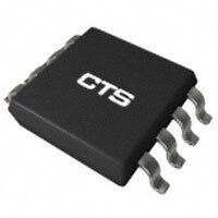
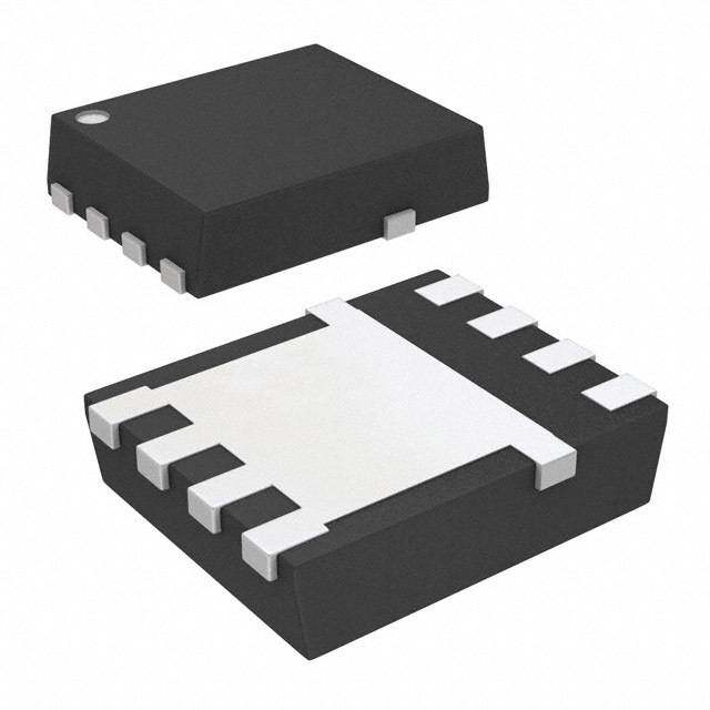
| 供应商器件封装 | 8-MSOP |
| 其它名称 | CTX1334TR |
| 包装 | 带卷 (TR) |
| 安装类型 | 表面贴装 |
| 封装/外壳 | 8-VSSOP,8-MSOP(0.118",3.00mm 宽) |
| 工作温度 | -40°C ~ 85°C |
| 应用 | - |
| 延迟时间 | 400ps |
| 数据速率(最大值) | - |
| 标准包装 | 1,000 |
| 特色产品 | http://www.digikey.cn/product-highlights/zh/semiconductors/52144 |
| 电压-电源 | 3 V ~ 5.5 V |
| 电容-输入 | - |
| 电流-电源 | 48mA |
| 类型 | 缓冲器, 转接驱动器 |
| 输入 | LVDS,LVPECL |
| 输出 | LVDS,LVPECL |
| 通道数 | 1 |


PDF Datasheet 数据手册内容提取
CTSLV 399 LVPECL/LVDS Oscillator Gain Stage & Buffer with Selectable Enable Not recommended for new designs MLP8, MSOP8 FEATURES BLOCK DIAGRAM Minimizes External Components Selectable Enable Polarity and Threshold (CMOS or PECL) 3V to 5.5V Power Supply Similar Operation as CTS100LVEL16VT Except with LVDS Outputs DESCRIPTION The CTSLV399 is a specialized oscillator gain stage with an LVDS output buffer including an enable. The selectable enable input allows continuous oscillator operation by only controlling the Q /Q¯ outputs. HG HG The CTSLV399 provides adjustable internal pull-down current sources for the Q/Q¯ outputs. Internal input biasing further reduces the number of needed external components ENGINEERING NOTES The CTSLV399 is a specialized oscillator gain stage with LVDS output buffer including an enable. The enable input (EN) allows continuous oscillator operation by only controlling the Q /Q¯ outputs. HG HG The CTSLV399 also provides a V and 470 internal bias resistors from D to V and D¯ to V . The V BB BB BB BB pin can support 1.5 mA sink/source current. Bypassing V to ground with a 0.01 F capacitor is BB recommended. Functionality MLP8 Package (CTSLV399NG) The MLP8, NG options of the CTSLV399, provide a PECL/ECL level enable input (¯E¯N¯). When the ¯E¯N¯ input is LOW, the Q¯ and QHG/Q¯HG outputs pass data from the inputs. When ¯E¯N¯ is HIGH, the Q¯ output continues to pass data while the Q output is forced high and the Q¯ output is forced low. HG HG Only the Q¯ output operates with a current source (4 mA) to V . This is accomplished by internal bonding EE of CS-SEL. An external resistor may also be used to increase pull-down current to a maximum of 25mA (includes 4mA on-chip current source). The CTSLV399NB and CTSLV399ND versions operate with a single ended data input (D). The D¯ input is internally bonded directly to the V pin bypassing the 470 bias resistor. BB Functionality MLP8 Package (CTSLV399N) & MSOP8 Package (CTSLV399T) The MSOP8 (T) and MLP8 (N) versions of the CTSLV399 provide a CMOS/TTL level enable input (EN). When the EN input is HIGH, the Q¯ and Q /Q¯ outputs pass data from the inputs. When EN is LOW, the HG HG Q¯ output continues to pass data while the Q output is forced high and the Q¯ output is forced low. HG HG Only the Q¯ output operates with a current source (4 mA) to V . This is accomplished by internal bonding EE of CS-SEL. An external resistor may also be used to increase pull-down current to a maximum of 25mA (includes 4mA on-chip current source). The MSOP8 (T) and MLP8 (N) CTSLV399 operates with a single ended data input (D). The D¯ input is internally bonded directly to the V pin bypassing the 470bias resistor. BB North Americas: +1-800-757-6686 • International: +1-508-435-6831 • Asia: +65-655-17551 • www.ctscorp.com/semiconductors Specifications are subject to change without notice. 1 RevA0215
CTSLV 399 LVPECL/LVDS Oscillator Gain Stage & Buffer with Selectable Enable Not recommended for new designs MLP8, MSOP8 Enable Truth Table EN-SEL EN/ EN Q/Q¯ Q Q¯ HG HG PECL Low, V or NC Data Data Data EE NC PECL High or V Data High Low CC CMOS/TTL Low, V or NC Data High Low V 1 EE EE CMOS/TTL High or V 2 Data Data Data CC 1 EN-SEL connections must be less than 1Ω. An external ≤ 20kΩ pull-up resistor between EN and V ensures a High when the 2 CC EN pin is not driven. Timing Diagram Current Source Truth Table CS-SEL Q Q¯ NC 4mA typ 4mA typ V 1 8mA typ 8mA typ EE V 1 0 4mA typ CC 1 Connection must be less than 1Ω. North Americas: +1-800-757-6686 • International: +1-508-435-6831 • Asia: +65-655-17551 • www.ctscorp.com/semiconductors Specifications are subject to change without notice. 2 RevA0215
CTSLV 399 LVPECL/LVDS Oscillator Gain Stage & Buffer with Selectable Enable Not recommended for new designs MLP8, MSOP8 Application Circuit for CMOS inputs Recommended Component Values for CMOS Single Ended Inputs R11 Value Input Type AC Coupled (C2 in DC Coupled (C2 circuit) shorted) 3.3 V CMOS 1.1 kΩ 2.0 kΩ 5.0 V CMOS 1.6 kΩ 3.3 kΩ R1 should be chosen so that the input swing on the D input with respect to D¯ is in the range of ±80 to ±1000 mV, per the AC Characteristics table and the D input is < ±750 mV with respect to V . BB North Americas: +1-800-757-6686 • International: +1-508-435-6831 • Asia: +65-655-17551 • www.ctscorp.com/semiconductors Specifications are subject to change without notice. 3 RevA0215
CTSLV 399 LVPECL/LVDS Oscillator Gain Stage & Buffer with Selectable Enable Not recommended for new designs MLP8, MSOP8 S11, 50Ω AC load S12, 50Ω AC load North Americas: +1-800-757-6686 • International: +1-508-435-6831 • Asia: +65-655-17551 • www.ctscorp.com/semiconductors Specifications are subject to change without notice. 4 RevA0215
CTSLV 399 LVPECL/LVDS Oscillator Gain Stage & Buffer with Selectable Enable Not recommended for new designs MLP8, MSOP8 S21, 50Ω AC load S22, 50Ω AC load North Americas: +1-800-757-6686 • International: +1-508-435-6831 • Asia: +65-655-17551 • www.ctscorp.com/semiconductors Specifications are subject to change without notice. 5 RevA0215
CTSLV 399 LVPECL/LVDS Oscillator Gain Stage & Buffer with Selectable Enable Not recommended for new designs MLP8, MSOP8 E lectrical Specifications Absolute Maximum Ratings are those values beyond which device life may be impaired. Symbol Characteristic Condition Rating Unit V PECL Power Supply V = 0V 0 to + 6.0 V CC EE V PECL Input Voltage V = 0V 0 to + 6.0 V I EE Referenced to V D/D¯ Input Voltage ±0.75 V D/ V BB Continuous Q/Q¯ 25 Surge Q/Q¯ 50 IOUT Output Current Continuous mA 5 Q /Q¯ HG HG Surge Q /Q¯ 10 HG HG T Operating Temperature Range - -40 to +85 °C A T Storage Temperature Range - -65 to +150 °C STG ESD Human Body Model Electro Static Discharge - 2500 V HBM ESD Machine Model Electro Static Discharge - 200 V MM ESD Charged Device Model Electro Static Discharge - 2000 V CDM 100K LVPECL DC Characteristics (V = GND, V = +3.3V) EE CC -40°C 0°C 25°C 85°C Symbol Characteristic Unit Min Max Min Max Min Max Min Max V Output HIGH Voltage1,2 2255 2465 2275 2465 2275 2465 2275 2465 mV OH V Output LOW Voltage1,2 1375 1745 1400 1680 1400 1680 1400 1680 mV OL Input HIGH Voltage D,EN 2135 2560 2135 2560 2135 2560 2135 2560 mV (EN-SEL open)1 V IH Input HIGH Voltage EN 2000 V 2000 V 2000 V 2000 V mV (EN-SEL tied to V )1 CC CC CC CC EE Input LOW Voltage D,EN 1400 1825 1400 1825 1400 1825 1400 1825 mV (EN-SEL open)1 V IL Input LOW Voltage EN GND 800 GND 800 GND 800 GND 800 mV (EN-SEL tied to V )1 EE V Reference Voltage1 1910 2050 1910 2050 1910 2050 1910 2050 mV BB I Input HIGH Current EN3 150 150 150 150 µA IH I Input LOW Current EN3 0.5 0.5 0.5 0.5 µA IL I Power Supply Current2 48 48 48 48 mA EE 1 Voltage levels vary 1:1 with VCC. 2 Specified with CS-SEL open. 3 Specified with EN-SEL open. North Americas: +1-800-757-6686 • International: +1-508-435-6831 • Asia: +65-655-17551 • www.ctscorp.com/semiconductors Specifications are subject to change without notice. 6 RevA0215
CTSLV 399 LVPECL/LVDS Oscillator Gain Stage & Buffer with Selectable Enable Not recommended for new designs MLP8, MSOP8 100K PECL DC Characteristics (VEE = GND, VCC = +5.0V) -40°C 0°C 25°C 85°C Symbol Characteristic Unit Min Max Min Max Min Max Min Max V Output HIGH Voltage1,2 3955 4165 3975 4165 3975 4165 3975 4165 mV OH V Output LOW Voltage1,2 3075 3445 3100 3380 3100 3380 3100 3380 mV OL Input HIGH Voltage D,EN 3835 4260 3835 4260 3835 4260 3835 4260 mV (EN-SEL open)1 V IH Input HIGH Voltage EN 2000 V 2000 V 2000 V 2000 V mV (EN-SEL tied to V )1 CC CC CC CC EE Input LOW Voltage D,EN 3100 3525 3100 3525 3100 3525 3100 3525 mV (EN-SEL open)1 V IL Input LOW Voltage EN GND 800 GND 800 GND 800 GND 800 mV (EN-SEL tied to V )1 EE V Reference Voltage1 3610 3750 3610 3750 3610 3750 3610 3750 mV BB I Input HIGH Current EN3 150 150 150 150 µA IH I Input LOW Current EN3 0.5 0.5 0.5 0.5 µA IL I Power Supply Current2 48 48 48 52 mA EE 1 Voltage levels vary 1:1 with VCC. 2 Specified with CS-SEL open. 3 Specified with EN-SEL open. LVDS DC Characteristics for Q /Q¯ Outputs1 (V = GND, V = +3.0V to +5.5V) HG HG EE CC -40(cid:31)C 0(cid:31)C 25(cid:31)C 85(cid:31)C Symbol Characteristic Unit Min Max Min Max Min Max Min Max V Output HIGH Voltage 1600 1600 1600 1600 mV OH V Output LOW Voltage 900 900 900 900 mV OL V Output Common Mode Voltage2 1125 1375 1125 1375 1125 1375 1125 1375 mV OC (cid:31)V Change in Common Mode Voltage3 -50 50 -50 50 -50 50 -50 50 mV OC V Single-Ended Output Swing 250 450 250 450 250 450 250 450 mV OUT V Differential Output Swing 500 900 500 900 500 900 500 900 mV DIFF_OUT 1 Specified with 100Ω resistor connecting QHG and Q¯HG together. 2 Common mode voltage is the center voltage between QHG and Q¯HG during a steady state. 3 Change in common mode voltage is the difference between common mode voltages at opposite binary states. North Americas: +1-800-757-6686 • International: +1-508-435-6831 • Asia: +65-655-17551 • www.ctscorp.com/semiconductors Specifications are subject to change without notice. 7 RevA0215
CTSLV 399 LVPECL/LVDS Oscillator Gain Stage & Buffer with Selectable Enable Not recommended for new designs MLP8, MSOP8 AC Characteristics (V = -3.0V to -5.5V; V =GND or V =GND; V = +3.0V to +5.5V) EE CC EE CC -40°C 0°C 25°C 85°C Symbol Characteristic Unit Min Typ Max Min Typ Max Min Typ Max Min Typ Max Propagation Delay tPLH/tPHL D to Q/Q¯1 400 400 400 430 ps D to Q /Q¯ 2 550 550 550 630 ps HG HG t Duty Cycle Skew3 5 20 5 20 5 20 5 20 ps SKEW V (AC) Input Swing4 80 1000 80 1000 80 1000 80 1000 mV PP Output Rise/Fall1 100 260 100 260 100 260 100 260 (20% - 80%) - Q tr/tf Output Rise/Fall1 (20% - 80%) - 180 280 180 280 180 280 180 280 ps Q HG 1 Specified with CS-SEL connected to VEE and Q/Q¯ with AC coupled 50Ω loads. 2 Specified with 100Ω resistor connecting Q and Q¯ together. HG HG 3 Duty cycle skew is the difference between a tPLH and tPHL propagation delay through a device. 4 The peak-to-peak differential input swing is the range for which AC parameters guaranteed. V and V must remain D within the range of ±750 mV with respect to V . BB North Americas: +1-800-757-6686 • International: +1-508-435-6831 • Asia: +65-655-17551 • www.ctscorp.com/semiconductors Specifications are subject to change without notice. 8 RevA0215
CTSLV 399 LVPECL/LVDS Oscillator Gain Stage & Buffer with Selectable Enable Not recommended for new designs MLP8, MSOP8 PACKAGE DIMENSIONS North Americas: +1-800-757-6686 • International: +1-508-435-6831 • Asia: +65-655-17551 • www.ctscorp.com/semiconductors Specifications are subject to change without notice. 9 RevA0215
CTSLV 399 LVPECL/LVDS Oscillator Gain Stage & Buffer with Selectable Enable Not recommended for new designs MLP8, MSOP8 P in Description and Configuration Pin Assignments for CTSLV399NG Pin Name Type Function 1 Q¯ Output Inverting PECL Output 2 D Input Data Input 3 V Output Reference Voltage BB 4 EN Input Output Enable 5 V Power Negative Supply EE 6 Q¯ Output Inverting LVDS Output HG 7 Q Output LVDS Output HG 8 V Power Positive Supply CC Pin Assignments for CTSLV399TG Pin Name Type Function 1 Q¯ Output Inverting PECL Output 2 D Input Data Input 3 V Output Reference Voltage BB 4 EN Input Output Enable 5 V Power Negative Supply EE 6 Q¯ Output Inverting LVDS Output HG 7 Q Output LVDS Output HG 8 V Power Positive Supply CC PART ORDERING INFORMATION Part Number Package Marking CTSLV399NG MLP8 V1G / YWW CTSLV399TG MSOP8 HV99G / YYWW North Americas: +1-800-757-6686 • International: +1-508-435-6831 • Asia: +65-655-17551 • www.ctscorp.com/semiconductors Specifications are subject to change without notice. 10 RevA0215