ICGOO在线商城 > 集成电路(IC) > PMIC - LED 驱动器 > CAT4101TV-T75
 Datasheet下载
- 型号: CAT4101TV-T75
- 制造商: ON Semiconductor
- 库位|库存: xxxx|xxxx
- 要求:
| 数量阶梯 | 香港交货 | 国内含税 |
| +xxxx | $xxxx | ¥xxxx |
查看当月历史价格
查看今年历史价格
CAT4101TV-T75产品简介:
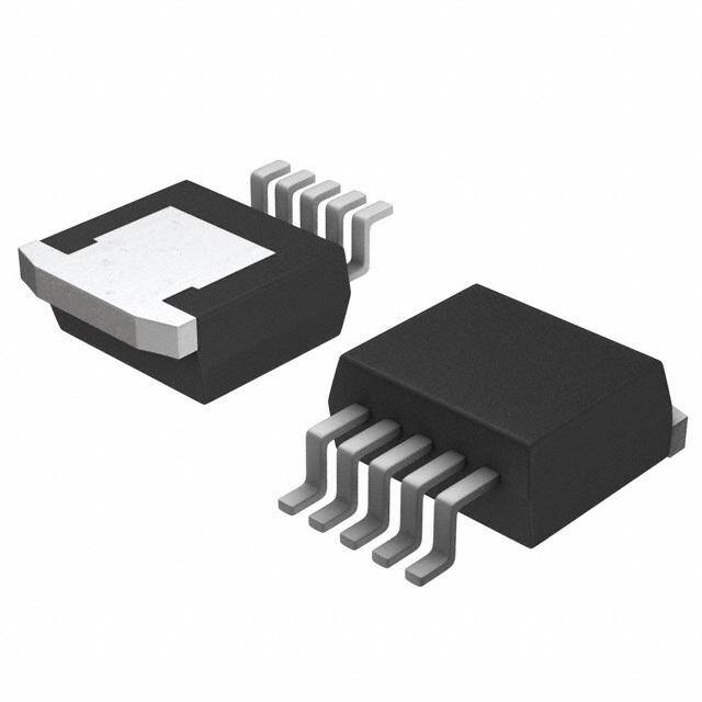
ICGOO电子元器件商城为您提供CAT4101TV-T75由ON Semiconductor设计生产,在icgoo商城现货销售,并且可以通过原厂、代理商等渠道进行代购。 CAT4101TV-T75价格参考。ON SemiconductorCAT4101TV-T75封装/规格:PMIC - LED 驱动器, LED Driver IC 1 Output Linear PWM Dimming 1A D²PAK-5 (TO-263-5)。您可以下载CAT4101TV-T75参考资料、Datasheet数据手册功能说明书,资料中有CAT4101TV-T75 详细功能的应用电路图电压和使用方法及教程。
ON Semiconductor(安森美)的CAT4101TV-T75是一款高效、恒流LED驱动器,属于PMIC-LED驱动器类别。该器件采用固定导通时间的迟滞控制架构,无需电感设计,适用于升压(Boost)或降压-升压(Buck-Boost)拓扑结构,特别适合驱动串联LED。

主要应用场景包括:

1. 便携式设备背光:广泛用于智能手机、平板电脑、MP3播放器等小型电子设备的LCD屏幕背光驱动,提供稳定亮度和高效率。

2. 手持照明设备:适用于LED手电筒、应急灯等电池供电照明产品,支持单节锂电池输入(2.7V–5.5V),能高效驱动多颗串联白光LED。

3. 消费类电子产品:如数码相机闪光灯、玩具灯、装饰照明等需要紧凑、高效LED驱动方案的场合。

4. 工业与指示照明:用于仪表盘背光、状态指示灯、小型面板照明等对空间和功耗敏感的应用。

CAT4101TV-T75采用SOT-23-6小尺寸封装,集成度高,外围元件少,有助于节省PCB空间;具备过温保护、短路保护等功能,提升系统可靠性。其高达90%以上的转换效率和低静态电流特性,延长了电池续航时间,非常适合对能效和体积要求严格的便携式应用。
| 参数 | 数值 |
| 产品目录 | 集成电路 (IC)光电子产品 |
| 描述 | IC LED DRVR HP CONST CURR D2PAKLED照明驱动器 1A Constant Crnt LED |
| 产品分类 | |
| 品牌 | ON Semiconductor |
| 产品手册 | |
| 产品图片 |
|
| rohs | 符合RoHS无铅 / 符合限制有害物质指令(RoHS)规范要求 |
| 产品系列 | LED照明电子器件,LED照明驱动器,ON Semiconductor CAT4101TV-T75- |
| 数据手册 | |
| 产品型号 | CAT4101TV-T75 |
| 产品目录页面 | |
| 产品种类 | LED照明驱动器 |
| 供应商器件封装 | TO-263-5 |
| 其它名称 | CAT4101TV-T75DKR |
| 内部驱动器 | 是 |
| 包装 | Digi-Reel® |
| 商标 | ON Semiconductor |
| 安装类型 | 表面贴装 |
| 安装风格 | SMD/SMT |
| 封装 | Reel |
| 封装/外壳 | TO-263-6,D²Pak(5 引线+接片),TO-263BA |
| 封装/箱体 | TO-263 |
| 工作温度 | -40°C ~ 85°C |
| 工厂包装数量 | 750 |
| 恒压 | - |
| 恒流 | 是 |
| 拓扑 | PWM |
| 最大工作温度 | + 85 C |
| 最大电源电流 | 1 A |
| 最小工作温度 | - 40 C |
| 标准包装 | 1 |
| 特色产品 | http://www.digikey.com/cn/zh/ph/Catalyst/cat4101.html |
| 电压-电源 | 3 V ~ 5.5 V |
| 电压-输出 | 25V |
| 类型-初级 | 车载,通用 |
| 类型-次级 | 高亮度 LED(HBLED),白色 LED |
| 系列 | CAT4101 |
| 输入电压 | 3 V to 5.5 V |
| 输出数 | 1 |
| 频率 | - |


- 商务部:美国ITC正式对集成电路等产品启动337调查
- 曝三星4nm工艺存在良率问题 高通将骁龙8 Gen1或转产台积电
- 太阳诱电将投资9.5亿元在常州建新厂生产MLCC 预计2023年完工
- 英特尔发布欧洲新工厂建设计划 深化IDM 2.0 战略
- 台积电先进制程称霸业界 有大客户加持明年业绩稳了
- 达到5530亿美元!SIA预计今年全球半导体销售额将创下新高
- 英特尔拟将自动驾驶子公司Mobileye上市 估值或超500亿美元
- 三星加码芯片和SET,合并消费电子和移动部门,撤换高东真等 CEO
- 三星电子宣布重大人事变动 还合并消费电子和移动部门
- 海关总署:前11个月进口集成电路产品价值2.52万亿元 增长14.8%


PDF Datasheet 数据手册内容提取
CAT4101 1 A Constant-Current LED Driver with PWM Dimming Description The CAT4101 is a constant−current sink driving a string of high−brightness LEDs up to 1 A with very low dropout of 0.5 V at full http://onsemi.com load. It requires no inductor, provides a low noise operation and minimizes the number of components. The LED current is set by an external resistor connected to the RSET pin. The LED pin is D2PAK 5 compatible with high voltage up to 25 V, allowing the driving of long (TO−263, 5 LEAD) strings of LEDs. The device ensures an accurate and regulated current TV SUFFIX in the LEDs independent of supply and LED forward voltage CASE 418AH variation. The PWM/EN input allows the device shutdown and the LED PIN CONNECTIONS brightness adjustment by using an external pulse width modulation (PWM) signal. 1 EN/PWM The driver features a thermal shutdown protection that becomes active whenever the die temperature exceeds 150°C. VIN TAB GND The device is available in a high−power, 5−lead TO−263 package offering excellent thermal dissipation characteristics. RSET LED Features • (Top View) Accurate 1 A Current Sink • Up to 25 V Operation on LED Pin • MARKING DIAGRAM Low Dropout 500 mV at 1 A • LED Current Set by External Resistor • High Resolution PWM Dimming via EN/PWM • CAT4101TV “Zero” Current Shutdown Mode XXXXXXXXX • Thermal Shutdown Protection • TO−263 (D2PAK) 5−lead Package • This Device is Pb−Free, Halogen Free/BFR Free and is RoHS 1 Compliant CAT4101TV = Specific Device Code XXXXXXXXX = Internal Traceability Applications • High Power LED up to 1 A • Architectural and General Lighting ORDERING INFORMATION • Automotive Lighting Device Package Shipping† VCC CAT4101TV−T75 TO−263 750 / 3 V to 25 V LEDs (D2PAK, 5 Lead) Tape & Reel (Pb−Free) 1 A VIN †For information on tape and reel specifications, VIN 5 V including part orientation and tape sizes, please CAT4101 refer to our Tape and Reel Packaging Specification OFF ON EN/PWM LED Brochure, BRD8011/D. RSET GND 549 (cid:2) Figure 1. Typical Application Circuit © Semiconductor Components Industries, LLC, 2012 1 Publication Order Number: July, 2012 − Rev. 8 CAT4101/D
CAT4101 Table 1. ABSOLUTE MAXIMUM RATINGS Parameter Rating Units VIN, RSET, EN/PWM Voltages 6 V LED Voltage 25 V Storage Temperature Range −65 to +150 (cid:2)C Junction Temperature Range −40 to +150 (cid:2)C Lead Temperature 300 (cid:2)C Stresses exceeding Maximum Ratings may damage the device. Maximum Ratings are stress ratings only. Functional operation above the Recommended Operating Conditions is not implied. Extended exposure to stresses above the Recommended Operating Conditions may affect device reliability. Table 2. RECOMMENDED OPERATING CONDITIONS Parameter Rating Units VIN Voltage 3.0 to 5.5 V LED Pin Voltage V device enabled, continuous operation Up to 6 device disabled or transient when enabled Up to 25 Ambient Temperature Range −40 to +85 (cid:2)C LED Pin Current Up to 1 A NOTE: Typical application circuit with external components is shown on page 1. 1. For additional temperature options, please contact your nearest ON Semiconductor Sales office. Table 3. ELECTRICAL OPERATING CHARACTERISTICS (Min and Max values in bold are over recommended operating conditions unless specified otherwise. Typical values are at VIN = 5.0 V, TAMB = 25°C) Symbol Parameter Conditions Min Typ Max Units ILED−ACC LED Current Accuracy VLED = 1 V, RSET = 1.47 k(cid:2) 315 350 385 mA VLED = 1 V, RSET = 750 (cid:2) 700 VLED = 1 V, RSET = 549 (cid:2) 1000 VDOUT Dropout Voltage ILED = 1 A 500 mV VRSET RSET Pin Voltage 1.17 1.20 1.23 V IQ Quiescent Current No LED, RSET = Floating 0.8 mA No LED, RSET = 549 (cid:2) 8.0 IQSHDN Shutdown Current VEN = 0 V 1 (cid:3)A EN/PWM Pin REN/PWM − Pull−down resistance 200 k(cid:2) VHI − Logic High Level 1.3 V VLO − Logic Low Level 0.4 V TSD Thermal Shutdown 150 (cid:2)C THYS Thermal Hysteresis 20 (cid:2)C ILED/IRSET RSET to LED Current gain ratio 100 mA LED current 400 VUVLO Undervoltage lockout (UVLO) Threshold 2.0 V http://onsemi.com 2
CAT4101 Table 4. RECOMMENDED EN/PWM TIMING (For 3.0 V ≤ VIN ≤ 5.5 V, over full ambient temperature range −40°C to +85°C.) Symbol Name Conditions Min Typ Max Units TPS Turn−On time, EN/PWM rising to ILED from ILED = 1 A 1.6 (cid:3)s Shutdown ILED = 350 mA 1.1 TP1 Turn−On time, EN/PWM rising to ILED ILED = 1 A 920 ns ILED = 350 mA 620 TP2 Turn−Off time, EN/PWM falling to ILED ILED = 1 A 440 ns ILED = 350 mA 310 TR LED rise time ILED = 1 A 840 ns ILED = 350 mA 390 TF LED fall time ILED = 1 A 470 ns ILED = 350 mA 350 TLO EN/PWM low time 1 (cid:3)s THI EN/PWM high time 5 (cid:3)s TPWRDWN EN/PWM low time to shutdown delay 8 ms THI TPWRDWN TLO EN/PWM SHUTDOWN SHUTDOWN TP2 TF TPS TP1 TR ILED = (1.2 V / RSET) x 400 90% LED CURRENT 50% 50% 10% SHUTDOWN 0 mA 0 mA VIN QUIESCENT CURRENT SHUTDOWN 0 mA SHUTDOWN Figure 2. CAT4101 EN/PWM Timing EN/PWM Operation The EN/PWM pin has two primary functions. One When performing a combination of low frequencies and function enables and disables the device. The other function small duty cycles, the device may enter shutdown mode. turns the LED channel on and off for PWM dimming This has no effect on the dimming accuracy, because the control. The device has a very fast turn−on time (from turn−on time T is very short, in the range of 1 (cid:3)s. PS EN/PWM rising to LED on) and allows “instant on” when To ensure that PWM pulses are recognized, pulse width dimming LED using a PWM signal. low time T should be longer than 1 (cid:3)s. The CAT4101 LO Accurate linear dimming is compatible with PWM enters a “zero current” shutdown mode after a 5 ms delay frequencies from 100 Hz to 5 kHz for PWM duty cycle (typical) when EN/PWM is held low. down to 1%. PWM frequencies up to 50 kHz can be supported for duty cycles greater than 10%. http://onsemi.com 3
CAT4101 TYPICAL PERFORMANCE CHARACTERISTICS (VIN = 5 V, VCC = 5 V, VF = 3.5 V, ILED = 1 A (1 LED), CIN = 1 (cid:3)F, TAMB = 25°C unless otherwise specified.) 1.2 8.0 No Load A) A) m m T ( 1.0 T ( 6.0 N N E E R R R R U U C 0.8 C 4.0 T T N N E E C C S S E 0.6 E 2.0 UI UI Q Q 0.4 0 3.0 3.5 4.0 4.5 5.0 5.5 0 200 400 600 800 1000 INPUT VOLTAGE (V) LED CURRENT (mA) Figure 3. Quiescent Current vs. VIN Voltage Figure 4. Quiescent Current vs. LED Current (I = 0 mA) LED 8.5 1.2 Full Load A) 1.0 m ENT ( 8.0 T (A) 0.8 R N R E CU 7.5 RR 0.6 T U N C CE ED 0.4 ES 7.0 L UI Q 0.2 6.5 0 3.0 3.5 4.0 4.5 5.0 5.5 0 0.3 0.6 0.9 1.2 1.5 INPUT VOLTAGE (V) LED PIN VOLTAGE (V) Figure 5. Quiescent Current vs. VIN Voltage Figure 6. LED Current vs. LED Pin Voltage (Full Load) 1.2 1.2 1.1 1.1 1.0 1.0 A) A) T ( 0.9 T ( 0.9 N N E 0.8 E 0.8 R R R R U 0.7 U 0.7 C C D 0.6 D 0.6 E E L L 0.5 0.5 0.4 0.4 0.3 0.3 2.0 2.5 3.0 3.5 4.0 4.5 5.0 5.5 −40 0 40 80 120 INPUT VOLTAGE (V) TEMPERATURE (°C) Figure 7. LED Current Change vs. VIN Voltage Figure 8. LED Current Change vs. Temperature http://onsemi.com 4
CAT4101 TYPICAL PERFORMANCE CHARACTERISTICS (VIN = 5 V, VCC = 5 V, VF = 3.5 V, ILED = 1 A (1 LED), CIN = 1 (cid:3)F, TAMB = 25°C unless otherwise specified.) 1.30 1.30 V) 1.25 V) 1.25 E ( E ( G G A A T T L 1.20 L 1.20 O O V V T T E E S S R 1.15 R 1.15 1.10 1.10 3.0 3.5 4.0 4.5 5.0 5.5 −40 0 40 80 120 INPUT VOLTAGE (V) TEMPERATURE (°C) Figure 9. RSET Pin Voltage vs. VIN Voltage Figure 10. RSET Pin Voltage vs. Temperature 1.2 1.0 A) T ( 0.8 N E R R 0.6 U C D 0.4 E L 0.2 0 0 1 2 3 4 5 RSET (k(cid:2)) Figure 11. LED Current vs. RSET Resistor Figure 12. PWM 200 Hz, 1% Duty Cycle 100 1.4 V) 1.2 %) D ( D CURRENT ( 110 LE THRESHOL 01..80 −284550°°°CCC E B L A 100 Hz EN 0.6 1 kHz 5 kHz 50 kHz 0.1 0.4 0.1 1 10 100 3.0 3.5 4.0 4.5 5.0 5.5 DUTY CYCLE (%) INPUT VOLTAGE (V) Figure 13. LED Current vs. PWM Duty Cycle Figure 14. EN/PWM Threshold vs. VIN http://onsemi.com 5
CAT4101 Table 5. PIN DESCRIPTIONS Name Pin Function EN/PWM 1 Device enable (active high) and PWM control. VIN 2 Device supply input, connect to battery or supply. GND 3 Ground reference. RSET 4 A resistor connected between this pin and ground sets the LED current. LED 5 Bottom LED cathode terminal. TAB – Connect TAB to the Ground plane. Pin Function VIN is the supply pin for the device. A small 0.1 (cid:3)F ceramic high−impedance zero−current state whenever the device is bypass capacitor is optional for noisy environments. The placed in shutdown mode. maximum operating voltage is 6.0 V. Whenever the input RSET pin is connected to an external resistor to set the LED supply falls below the under−voltage threshold, the current current. The ground side of the external resistor should be sink will automatically be disabled. star connected to the GND of the PCB. The pin source EN/PWM is the enable and one wire dimming input for the current mirrors the current to the LED sink. The voltage at LED channel. Guaranteed levels of logic high and logic low this pin is regulated to 1.2 V. are set at 1.3 V and 0.4 V respectively. When EN/PWM is GND is the ground reference for the device. The pin must be initially taken high, the device becomes enabled and the connected to the ground plane on the PCB. LED current is set at a gain of 400 times the current in RSET. TAB is the exposed pad underneath the package. For best To place the device into zero current shutdown mode, the thermal performance, the tab should be soldered to the PCB EN/PWM pin must be held low for 5 ms typical. and connected to the ground plane. LED pin is connected to the bottom LED cathode and provides a regulated current sink. The pin enters a http://onsemi.com 6
CAT4101 Block Diagram VIN LED Undervoltage & Thermal VIN Lockout EN/PWM Shutdown Delay Reference Voltage Current Regulator RSET RSET Regulator & Mirror GND Figure 15. CAT4101 Functional Block Diagram Basic Operation Table 6. RSET RESISTOR SETTINGS The CAT4101 has one highly accurate LED current sink LED Current [mA] RSET [(cid:2)] to regulate LED current in a string of LEDs. The LED current is mirrored from the current flowing from the RSET 100 4990 pin. Table 6 lists various RSET resistor values for LED 200 2490 current in 100 mA increments. 300 1690 The LED channel needs a minimum of 500 mV headroom 400 1270 to sink constant regulated current. If the input supply falls below 2 V, the under−voltage lockout circuit disables the 500 1050 LED channel. 600 866 For applications requiring current higher than 1 A, several 700 768 CAT4101 devices can be connected in parallel. The LED channel can withstand and operate at voltages 800 680 up to 25 V. This makes the device ideal for driving long 900 604 strings of high power LEDs from a high voltage source. 1000 549 http://onsemi.com 7
CAT4101 Application Information Single 12 V Supply For a given package style and board layout, the operating The circuit shown in Figure 16 shows how to power three junction temperature TJ is a function of the power LEDs in series from a single 12 V supply using the dissipation P , and the ambient temperature, resulting in the D CAT4101. The CAT4101 can not be driven directly from following equation: 12 V, three components are needed to create a lower voltage T (cid:2)T (cid:4)P ((cid:4) (cid:4)(cid:4) )(cid:2)T (cid:4)P (cid:4) for the VIN pin (below 5.5 V). Resistor R2 and zener diode J AMB D JC CA AMB D JA The CAT4101 TO−263 5−lead package provides a thermal D provide a regulated voltage while the quiescent current resistance when the ground tab is soldered down to the PCB. runs through the N−Channel transistor M. Suitable parts for When mounted on a double−sided printed circuit board with this circuit are the ON Semiconductor MM3Z6V2 zener two square inches of copper allocated for “heat spreading”, diode and the 2N7002L N−channel transistor (SOT23 package). the resulting (cid:4)JA is about 30°C/W. For example, at 60°C ambient temperature, the maximum power dissipation is calculated as follow: 12 V 1 C(cid:3)F2 5 Rk(cid:2)2 P (cid:2)TJmax(cid:5)TAMB(cid:2)150(cid:5)60(cid:2)3W M Dmax (cid:4)JA 30 D 6.2 V Recommended Layout VIN LED The board layout should provide good thermal dissipation C1 0.1 (cid:3)F through the PCB. Multiple via can be used to connect the tab CAT4101 of the CAT4101 to a large ground plane underneath the package. EN/PWM Input capacitor C1 should be placed as close to the driver RSET IC as possible. The RSET resistor should have a Kelvin GND connection to the GND pin of the CAT4101. R1 Figure 16. Single Supply Driving Three LEDs Power Dissipation The power dissipation (P ) of the CAT4101 can be D calculated as follows: P (cid:2)(V (cid:3)I )(cid:4)(V (cid:3)I ) D IN IN LED LED where V is the voltage at the LED pin. Combinations of LED high V voltage or high ambient temperature can cause LED the CAT4101 to enter thermal shutdown. In applications where V is high, a resistor can be inserted in series with LED the LED string to lower P . D Thermal dissipation of the junction heat consists primarily of two paths in series. The first path is the junction to the case ((cid:4) ) thermal resistance which is defined by the JC package style, and the second path is the case to ambient ((cid:4) ) thermal resistance, which is dependent on board CA layout. The overall junction to ambient ((cid:4) ) thermal JA resistance is equal to: (cid:4) (cid:2)(cid:4) (cid:4)(cid:4) Figure 17. CAT4101 Recommended Layout JA JC CA http://onsemi.com 8
CAT4101 PACKAGE DIMENSIONS D2PAK−5 (TO−263, 5 LEAD) CASE 418AH−01 ISSUE A B SEATING PLANE A E A NOTES: 1. DIMENSIONING AND TOLERANCING PER ASME L1 c2 Y14.5M, 1994. 2. CONTROLLING DIMENSION: MILLIMETERS. 3. DIMENSIONS D AND E DO NOT INCLUDE MOLD FLASH AND GATE PROTRUSIONS. MOLD FLASH AND GATE PROTRUSIONS NOT TO EXCEED 0.13 MAXIMUM PER SIDE. THESE DIMENSIONS D TO BE MEASURED AT DATUM H. H DETAIL A MILLIMETERS DIM MIN MAX A 4.06 4.82 A1 0.00 0.25 b 0.51 0.99 c 0.33 0.74 c2 1.14 1.65 c D 8.38 9.65 e BOTTOM VIEW E 9.65 10.67 5Xb SIDE VIEW e 1.70 BSC H 14.61 15.88 0.13 M B AM TOP VIEW H L 1.78 2.79 L1 −−− 1.68 M 0 (cid:2) 8 (cid:2) M RECOMMENDED SOLDERING FOOTPRINT* 10.80 L A1 B SPELAATNIENG DETAIL A 8.60 16.00 4.20 1.70 5X1.00 PITCH DIMENSIONS: MILLIMETERS *For additional information on our Pb−Free strategy and soldering details, please download the ON Semiconductor Soldering and Mounting Techniques Reference Manual, SOLDERRM/D. ON Semiconductor and are registered trademarks of Semiconductor Components Industries, LLC (SCILLC). SCILLC owns the rights to a number of patents, trademarks, copyrights, trade secrets, and other intellectual property. A listing of SCILLC’s product/patent coverage may be accessed at www.onsemi.com/site/pdf/Patent−Marking.pdf. SCILLC reserves the right to make changes without further notice to any products herein. SCILLC makes no warranty, representation or guarantee regarding the suitability of its products for any particular purpose, nor does SCILLC assume any liability arising out of the application or use of any product or circuit, and specifically disclaims any and all liability, including without limitation special, consequential or incidental damages. “Typical” parameters which may be provided in SCILLC data sheets and/or specifications can and do vary in different applications and actual performance may vary over time. All operating parameters, including “Typicals” must be validated for each customer application by customer’s technical experts. SCILLC does not convey any license under its patent rights nor the rights of others. SCILLC products are not designed, intended, or authorized for use as components in systems intended for surgical implant into the body, or other applications intended to support or sustain life, or for any other application in which the failure of the SCILLC product could create a situation where personal injury or death may occur. Should Buyer purchase or use SCILLC products for any such unintended or unauthorized application, Buyer shall indemnify and hold SCILLC and its officers, employees, subsidiaries, affiliates, and distributors harmless against all claims, costs, damages, and expenses, and reasonable attorney fees arising out of, directly or indirectly, any claim of personal injury or death associated with such unintended or unauthorized use, even if such claim alleges that SCILLC was negligent regarding the design or manufacture of the part. SCILLC is an Equal Opportunity/Affirmative Action Employer. This literature is subject to all applicable copyright laws and is not for resale in any manner. PUBLICATION ORDERING INFORMATION LITERATURE FULFILLMENT: N. American Technical Support: 800−282−9855 Toll Free ON Semiconductor Website: www.onsemi.com Literature Distribution Center for ON Semiconductor USA/Canada P.O. Box 5163, Denver, Colorado 80217 USA Europe, Middle East and Africa Technical Support: Order Literature: http://www.onsemi.com/orderlit Phone: 303−675−2175 or 800−344−3860 Toll Free USA/Canada Phone: 421 33 790 2910 Fax: 303−675−2176 or 800−344−3867 Toll Free USA/Canada Japan Customer Focus Center For additional information, please contact your local Email: orderlit@onsemi.com Phone: 81−3−5817−1050 Sales Representative http://onsemi.com CAT4101/D 9
Mouser Electronics Authorized Distributor Click to View Pricing, Inventory, Delivery & Lifecycle Information: O N Semiconductor: CAT4101TV-T75