ICGOO在线商城 > 集成电路(IC) > PMIC - LED 驱动器 > LV52205MUTBG
 Datasheet下载
- 型号: LV52205MUTBG
- 制造商: ON Semiconductor
- 库位|库存: xxxx|xxxx
- 要求:
| 数量阶梯 | 香港交货 | 国内含税 |
| +xxxx | $xxxx | ¥xxxx |
查看当月历史价格
查看今年历史价格
LV52205MUTBG产品简介:
ICGOO电子元器件商城为您提供LV52205MUTBG由ON Semiconductor设计生产,在icgoo商城现货销售,并且可以通过原厂、代理商等渠道进行代购。 LV52205MUTBG价格参考。ON SemiconductorLV52205MUTBG封装/规格:PMIC - LED 驱动器, LED 驱动器 IC 1 输出 DC DC 稳压器 升压 PWM 调光 700mA(开关) 6-UDFN(2x2)。您可以下载LV52205MUTBG参考资料、Datasheet数据手册功能说明书,资料中有LV52205MUTBG 详细功能的应用电路图电压和使用方法及教程。
ON Semiconductor(安森美半导体)的LV52205MUTBG是一款专用LED驱动器,属于PMIC(电源管理集成电路)中的LED驱动器类别。该器件主要面向中、小尺寸LED背光应用,广泛用于便携式电子产品和消费类设备中。

典型应用场景包括:

1. 智能手机和平板电脑显示屏背光: LV52205MUTBG可为LCD或OLED屏幕提供高效、稳定的LED背光驱动,支持亮度调节功能,适应不同环境下的显示需求。

2. 数码相机与便携式游戏机: 在这些设备的显示屏中,该芯片可实现节能高效的背光控制,延长电池续航时间。

3. 车载信息娱乐系统(IVI)显示屏: 适用于车载小尺寸显示屏的背光驱动,具备一定的温度保护和故障检测功能,提高系统可靠性。

4. 工业与医疗手持设备: 如便携式检测仪器、手持终端等,需要低功耗、高稳定性的LED背光解决方案。

该芯片采用小型封装,集成度高,支持PWM调光和模拟调光方式,具有过温、过流保护功能,适合空间受限且对可靠性有要求的设计场景。
| 参数 | 数值 |
| 产品目录 | 集成电路 (IC)光电子产品 |
| 描述 | IC LED BOOST DVR PWM 6UDFNLED照明驱动器 LED |
| 产品分类 | |
| 品牌 | ON Semiconductor |
| 产品手册 | |
| 产品图片 | |
| rohs | 符合RoHS无铅 / 符合限制有害物质指令(RoHS)规范要求 |
| 产品系列 | LED照明电子器件,LED照明驱动器,ON Semiconductor LV52205MUTBG- |
| mouser_ship_limit | 该产品可能需要其他文件才能进口到中国。 |
| 数据手册 | |
| 产品型号 | LV52205MUTBG |
| PCN组件/产地 | |
| 产品 | LED Lighting Drivers |
| 产品种类 | LED照明驱动器 |
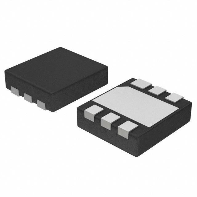
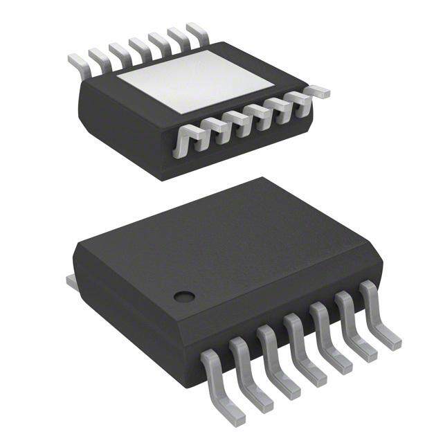
| 供应商器件封装 | 6-UDFN (2x2) |
| 其它名称 | LV52205MUTBGOSCT |
| 内部驱动器 | 是 |
| 功率耗散 | 2.05 W |
| 包装 | 剪切带 (CT) |
| 商标 | ON Semiconductor |
| 安装类型 | 表面贴装 |
| 安装风格 | SMD/SMT |
| 封装 | Reel |
| 封装/外壳 | 6-UFDFN 裸露焊盘 |
| 封装/箱体 | WDFN-6 |
| 工作温度 | -30°C ~ 85°C |
| 工作频率 | 600 kHz |
| 工厂包装数量 | 3000 |
| 恒压 | - |
| 恒流 | - |
| 拓扑 | PWM,升压(升压) |
| 拓扑结构 | PWM |
| 最大工作温度 | + 85 C |
| 最小工作温度 | - 30 C |
| 标准包装 | 1 |
| 电压-电源 | 2.7 V ~ 5.5 V |
| 电压-输出 | - |
| 类型-初级 | 背光 |
| 类型-次级 | - |
| 系列 | LV52205MU |
| 输入电压 | 2.7 V to 5.5 V |
| 输出数 | 1 |
| 输出类型 | Boost |
| 频率 | 600kHz |


- 商务部:美国ITC正式对集成电路等产品启动337调查
- 曝三星4nm工艺存在良率问题 高通将骁龙8 Gen1或转产台积电
- 太阳诱电将投资9.5亿元在常州建新厂生产MLCC 预计2023年完工
- 英特尔发布欧洲新工厂建设计划 深化IDM 2.0 战略
- 台积电先进制程称霸业界 有大客户加持明年业绩稳了
- 达到5530亿美元!SIA预计今年全球半导体销售额将创下新高
- 英特尔拟将自动驾驶子公司Mobileye上市 估值或超500亿美元
- 三星加码芯片和SET,合并消费电子和移动部门,撤换高东真等 CEO
- 三星电子宣布重大人事变动 还合并消费电子和移动部门
- 海关总署:前11个月进口集成电路产品价值2.52万亿元 增长14.8%


PDF Datasheet 数据手册内容提取
LV52205MU Bi-CMOS IC LED Boost Driver with PWM www.onsemi.com D imming Overview The LV52205MU is a high voltage boost driver for LED drive. LED current is set by the external resistor R1 and LED dimming can be done by changing FB voltage with PWM control. Feature Operating Voltage from 2.7V to 5.5V Integrated 42V MOSFET PWM dimming for Brightness Control 600kHz Switching Frequency UDFN6 2×2, 0.65P Typical Applications LED Display Backlight Control L1 D1 VBAT 22μH C1 C2 1μF 1μF PWM N M W VI W S P LV52205 P A D B C N F F G C3 220nF R1 10Ω ORDERING INFORMATION See detailed ordering and shipping information on page 12 of this data sheet. © Semiconductor Components Industries, LLC, 2015 1 Publication Order Number : J anuary 2015 - Rev. 1 LV52205MU/D
LV52205MU Specifications Absolute Maximum Ratings at Ta = 25C Parameter Symbol Conditions Ratings Unit Maximum supply voltage VCC max VCC 5.5 V Maximum pin voltage1 V1 max SW 42 V Maximum pin voltage2 V2 max Other pin 5.5 V Allowable power dissipation Pd max Ta = 25C *1 2.05 W Operating temperature Topr -30 to +85 C Storage temperature Tstg -55 to +125 C *1 Mounted on a specified board: 70mm50mm1.2mm (4 layer glass epoxy) Caution 1) Absolute maximum ratings represent the values which cannot be exceeded for any length of time. Caution 2) Even when the device is used within the range of absolute maximum ratings, as a result of continuous usage under high temperature, high current, high voltage, or drastic temperature change, the reliability of the IC may be degraded. Please contact us for the further details. StressesexceedingthoselistedintheMaximumRatingstablemaydamagethedevice.Ifanyoftheselimitsareexceeded,devicefunctionalityshouldnotbeassumed, damagemayoccurandreliabilitymaybeaffected. Recommendation Operating Condition at Ta = 25C Parameter Symbol Conditions Ratings Unit Supply voltage range1 VCC op VCC 2.7 to 5.5 V PWM frequency Fpwm 300 to 100k Hz FunctionaloperationabovethestresseslistedintheRecommendedOperatingRangesisnotimplied.ExtendedexposuretostressesbeyondtheRecommended OperatingRangeslimitsmayaffectdevicereliability. Electrical Characteristics Analog block at Ta 25C, VCC = 3.6V, unless otherwise specified Ratings Parameter Symbol Conditions Unit min typ max Standby current dissipation ICC1 SHUTDOWN 0 5 A DC/DC current dissipation ICC2 VOUT = 30V, ILED = 20mA 1 mA FB voltage Vfb PWM duty 100% 0.19 0.2 0.21 V FB pin leak current Ifb 1 A OVP voltage Vovp SW 40 41 42 V SWOUT ON resistance Ron IL = 100mA 700 m NMOS switch current limit ILIM Vfb = 200mV 0.7 A OSC frequency Fosc 600 kHz High level input voltage VINH PWM 1.5 VCC V Low level input voltage VINL PWM 0 0.4 V Under voltage lockout Vuvlo VIN falling 2.2 V PWM setup time from Ton 20 us shutdown PWM low time to shutdown Toff 8.9 ms ProductparametricperformanceisindicatedintheElectricalCharacteristicsforthelistedtestconditions,unlessotherwisenoted.Productperformancemaynotbe indicatedbytheElectricalCharacteristicsifoperatedunderdifferentconditions. www.onsemi.com 2
LV52205MU Block Diagram VBAT SW 4 VCC 6 UVLO OCP OVP 600kHz PWM TSD Controler 1 FB PWM 5 VREF VREF CONTROL GND FCAP 3 2 Pin Connections FB 1 6 VIN FCAP 2 5 PWM GND 3 4 SW Top view Pin Function PIN # Pin Name Description 1 FB Feedback pin. 2 FCAP Filtering capacitor terminal for PWM signal. 3 GND Ground 4 SW Switch pin. Drain of the internal power FET. 5 PWM PWM dimming input (active High). 6 VCC Supply voltage. Expose-pad Connect to GND on PCB. www.onsemi.com 3
LV52205MU Pd max -- Ta 3.0 Mounted on a specified board: 70×50×1.2mm3 W (4 layer glass epoxy) -- x a m n, Pd 2.0 2.05 o ati p ssi di er w 1.0 o p 0.82 e bl a w o All 0 --30 0 30 60 90 120 Ambient temperature,Ta -- C LED Current Setting LED current is set by an external resistor connected between the FB pin and ground. ILED = VFB/RFB. The VFB can be controled by PWM signal. PWM input is converted into a near DC current by the internal resistor R that was equivalent to 60k (±10%) and the external capacitor CFCAP as a low pass filter with a cut-off frequency fc = 1/2πRCFCAP. The VFB can be adjusted by altering the duty cycle of the PWM signal (See Fig.1). VFB = 200 (mV) PWM Duty (%) 200 180 160 140 V) 120 m (B 100 F V 80 60 40 20 0 0 10 20 30 40 50 60 70 80 90 100 PWM Duty (%) Fig1. VFB vs. PWM Duty www.onsemi.com 4
LV52205MU PWM Control DC-DC Delay max = 4.6ms Ton>20us Toff > 8.9ms PWM Shutdown PWM Enable DCDCENH (IC inside signal) FB Max 4ms @ Cfcap = 22nF (T.C.= 60k * Cfcap) FCAP The time until stable movement max = 8.6ms Fig2.Timing Diagram in PWM signal Open LED Protection If SW terminal voltage exceeds a threshold Vovp (41V typ) for 8 cycles, boost converter enters shutdown mode. In order to restart the IC, PWM setup signal is required again. Over Current Protection Current limit value for built-in power MOS is around 0.7A. The power MOS is turned off for each switching cycle when peak current through it exceeds the limit value. Under Voltage Lock Out (UVLO) UVLO operation works when VIN terminal voltage is below 2.2V. Thermal Shutdown When chip temperature is too high, boost converter is stopped. www.onsemi.com 5
LV52205MU Application Circuit Diagram 10LEDs L1 D1 VBAT 22μH C1 C2 1μF 1μF PWM 6 5 4 N M W VI W S P P A D B C N F F G 1 2 3 C3 220nF R1 10Ω L1: VLS3012T-220M49 (TDK), VLF504015MT-220M (TDK) D1: MBR0540T1 (ONsemi), NSR05F40 (ONsemi) C2: GRM21BR71H105K (Murata), C1608X5R1H105K (TDK) 6LEDs L1 D1 VBAT 10μH C1 C2 1μF 1μF PWM 6 5 4 N M W VI W S P P A D B C N F F G 1 2 3 C3 220nF R1 10Ω L1: VLS3012T-100M72 (TDK), VLF302512M-100M (TDK) D1: MBR0540T1 (ONsemi), NSR05F40 (ONsemi) C2: GRM21BR71H105K (Murata), C1608X5R1H105K (TDK) www.onsemi.com 6
LV52205MU Typical Characteristics (VIN = 3.6V, L = 22H, T = 25C, unless otherwise specified) Efficiency -- Output current Efficiency -- Output current 100 100 VIN=3.8V 10LED 90 90 8LED 4.2V ncy -- % 7800 10LED 11LED ncy -- % 7800 3.6V 3.0V Effice 60 Effice 60 50 50 40 40 0 5 10 15 20 0 5 10 15 20 LED current -- mA LED current -- mA FB voltage -- PWM duty FB voltage -- Temperature 200 200 Duty=100% 180 160 150 V V 140 m m ge -- 100 ge -- 110200 Duty=50% volta volta 80 FB FB 60 50 40 Duty=10% 20 0 0 0 10 20 30 40 50 60 70 80 90 100 --30 --15 0 15 30 45 60 75 90 PWM duty -- % Temperature -- °C LED current -- PWM frequency VIN current -- Temperature 20 1 75% 0.8 15 D current -- mA 10 50% I mA-- CC 00..46 E L 5 25% 0.2 0 0 0.1 1 10 100 -40 -20 0 20 40 60 80 100 PWM frequency -- kHz Temperature -- °C OVP voltage -- Temperature UVLO voltage -- Temperature 2.40 43 2.35 42 V VP voltage -V 434190 VLO voltage - 22..3205 O U 2.20 38 2.15 37 36 2.10 -40 -20 0 20 40 60 80 100 -40 -20 0 20 40 60 80 100 Temperature -- °C Temperature -- °C www.onsemi.com 7
LV52205MU PACKAGE DIMENSIONS UDFN6 2x2, 0.65P CASE 517AB NOTES: D A 1. DIMENSIONING AND TOLERANCING PER B ASME Y14.5M, 1994. 2. CONTROLLING DIMENSION: MILLIMETERS. 3. COPLANARITY APPLIES TO THE EXPOSED PAD AS WELL AS THE TERMINALS. MILLIMETERS DIM MIN MAX A 0.45 0.55 E A1 0.00 0.05 PIN ONE A3 0.127 REF REFERENCE b 0.25 0.35 D 2.00 BSC D2 1.50 1.70 2X 0.10 C E 2.00 BSC E2 0.80 1.00 e 0.65 BSC 2X 0.10 C K 0.20 --- L 0.25 0.35 A3 SOLDERING FOOTPRINT* 0.10 C A 6X 0.95 0.47 6X 0.08 C 6X A1 0.40 C SEATING 1 PLANE D2 6XL e 4X 1.70 1 3 E2 0.65 PITCH 2.30 6X K 6 4 6Xb DIMENSIONS: MILLIMETERS 0.10 C A B *For additional information on our Pb-Free strategy and soldering BOTTOM VIEW 0.05 C details, please download the ON Semiconductor Soldering and Mounting Techniques Reference Manual, SOLDERRM/D. LV52205MU is as follows. MARKING DIAGRAM 1 T5M T5 = Device Code M = Date Code = Pb−Free Package (Note: Microdot may be in either location) www.onsemi.com 8
LV52205MU Packing Specification of Embossed Carrier Taping UDFN6 (2.0×2.0) 3,000 pcs/reel .EMBOSSEDCARRIERTAPING - .Embossedcarriertapedimensions Embossment Sprockethole Unit• Fmm - .Tapemountingdirection Reel Indexmark EmbossedCarriertape Directionofunreeling www.onsemi.com 9
LV52205MU .TAPESTRENGTH - .Tensilestrengthofthecarriertape Min.10N - .Peelstrengthofthetopcovertape ( )Peelangle 165 to180 relativetothetapeadhesivesurface ( )Peelrate 300mm/minute ( )Peelofstrength 0.1Nto1.0N .PARTSNo.ONBARCODELABEL Typenumber T B G Directionindication LEADFREEsymbol .REELDIMENSIONS 1.6 MIN 10.9 MAX TYPE:P-RRM-08B UNIT:mm www.onsemi.com 10
LV52205MU Carriertape typenumber MaximumnumberofICscontained(pcs.) SANYOPackagecode Packingform Reel Innerbox Innerbox.B50766P001 3,000 30,000 10Reelscontained N22986D001 UDFN6(2.0*2.0) Dimensions:mm 190 136 186 MPNLabel 1 HOURS:UNLIMITED PackingMethod Innerbox Directionofunreeling MPNLabel Fixbytape Put10ReelintoInnerbox MPNSticher www.onsemi.com 11
LV52205MU ORDERING INFORMATION Device Package Shipping (Qty / Packing) UDFN6 (2x2) LV52205MUTBG (Pb-Free) 3000 / Tape & Reel ONSemiconductorandtheONlogoareregisteredtrademarksofSemiconductorComponentsIndustries,LLC(SCILLC)oritssubsidiariesintheUnitedStates and/orothercountries.SCILLCownstherightstoanumberofpatents,trademarks,copyrights,tradesecrets,andotherintellectualproperty.Alistingof SCILLC’sproduct/patentcoveragemaybeaccessedatwww.onsemi.com/site/pdf/Patent-Marking.pdf.SCILLCreservestherighttomakechangeswithout furthernoticetoanyproductsherein.SCILLCmakesnowarranty,representationorguaranteeregardingthesuitabilityofitsproductsforanyparticularpurpose, nordoesSCILLCassumeanyliabilityarisingoutoftheapplicationoruseofanyproductorcircuit,andspecificallydisclaimsanyandallliability,including withoutlimitationspecial,consequentialorincidentaldamages.“Typical”parameterswhichmaybeprovidedinSCILLCdatasheetsand/orspecificationscan anddovaryindifferentapplicationsandactualperformancemayvaryovertime.Alloperatingparameters,including“Typicals”mustbevalidatedforeach customerapplicationbycustomer’stechnicalexperts.SCILLCdoesnotconveyanylicenseunderitspatentrightsnortherightsofothers.SCILLCproductsare notdesigned,intended,orauthorizedforuseascomponentsinsystemsintendedforsurgicalimplantintothebody,orotherapplicationsintendedtosupportor sustainlife,orforanyotherapplicationinwhichthefailureoftheSCILLCproductcouldcreateasituationwherepersonalinjuryordeathmayoccur.Should Buyerpurchaseor useSCILLC productsforanysuchunintendedor unauthorizedapplication,BuyershallindemnifyandholdSCILLC anditsofficers, employees,subsidiaries,affiliates,anddistributorsharmlessagainstallclaims,costs,damages,andexpenses,andreasonableattorneyfeesarisingoutof, directlyorindirectly,anyclaimofpersonalinjuryordeathassociatedwithsuchunintendedorunauthorizeduse,evenifsuchclaimallegesthatSCILLCwas negligentregardingthedesignormanufactureofthepart.SCILLCisanEqual Opportunity/AffirmativeActionEmployer.Thisliteratureissubjecttoall applicable copyright laws and is not for resale in any manner. www.onsemi.com 12