ICGOO在线商城 > 集成电路(IC) > PMIC - LED 驱动器 > TPS61311YFFR
 Datasheet下载
- 型号: TPS61311YFFR
- 制造商: Texas Instruments
- 库位|库存: xxxx|xxxx
- 要求:
| 数量阶梯 | 香港交货 | 国内含税 |
| +xxxx | $xxxx | ¥xxxx |
查看当月历史价格
查看今年历史价格
TPS61311YFFR产品简介:
ICGOO电子元器件商城为您提供TPS61311YFFR由Texas Instruments设计生产,在icgoo商城现货销售,并且可以通过原厂、代理商等渠道进行代购。 TPS61311YFFR价格参考¥3.47-¥7.78。Texas InstrumentsTPS61311YFFR封装/规格:PMIC - LED 驱动器, LED 驱动器 IC 3 输出 DC DC 稳压器 升压 PWM 调光 1.5A(闪存) 20ピンDSBGA(2.1x2)。您可以下载TPS61311YFFR参考资料、Datasheet数据手册功能说明书,资料中有TPS61311YFFR 详细功能的应用电路图电压和使用方法及教程。
TPS61311YFFR 是 Texas Instruments(德州仪器)推出的一款 PMIC - LED 驱动器,专为低功耗和高效能的背光驱动应用设计。以下是其主要应用场景:

 1. 便携式电子设备
   - 智能手机和平板电脑:TPS61311YFFR 能够为中小尺寸 LCD 屏幕提供高效的背光驱动,支持单串白光 LED,适用于手机、平板电脑等移动设备。
   - 可穿戴设备:如智能手表、健身追踪器等,这些设备需要低功耗解决方案以延长电池续航时间,TPS61311 的高效率特性非常适合此类应用。

 2. 消费类电子产品
   - 数码相机和摄像机:在拍摄过程中,LCD 屏幕需要持续的背光支持,TPS61311 可以稳定地驱动 LED 并保持低功耗。
   - 便携式多媒体播放器:为屏幕提供均匀的亮度和稳定的电流输出,确保用户体验。

 3. 工业与医疗设备
   - 手持式测量设备:例如便携式示波器、万用表等,这些设备通常需要小型化设计和长续航能力。
   - 便携式医疗设备:如血糖仪、脉搏血氧仪等,TPS61311 提供的小型封装和高效性能能够满足严格的电源要求。

 4. 汽车电子
   - 车载信息娱乐系统:用于仪表盘或导航系统的显示屏背光驱动,支持宽输入电压范围(2.7V 至 5.5V),适应汽车电池供电环境。
   - 后视镜显示屏:为小型显示屏提供可靠的背光支持。

 5. 其他应用
   - 电子书阅读器:如 Kindle 等设备,TPS61311 的低静态电流特性有助于延长电池寿命。
   - 智能家居设备:如带屏幕的智能音箱、温控器等,提供高效且稳定的 LED 驱动。

 核心优势
- 高效率:高达 90% 的转换效率,减少功率损耗。
- 小尺寸:采用 6 引脚 SOT-23 封装,适合空间受限的设计。
- 简单易用:外部元件少,便于集成到各种系统中。
- 保护功能:内置短路保护和热关断功能,提升系统可靠性。

综上所述,TPS61311YFFR 主要应用于需要高效、低功耗 LED 驱动的各种便携式设备和小型化系统中,尤其适合对电池寿命有严格要求的产品。
| 参数 | 数值 |
| 产品目录 | 集成电路 (IC)光电子产品 |
| 描述 | IC LED FLASH DRVR I2C 20DSBGALED照明驱动器 1.5A Multiple LED Camera Flash Drvr |
| 产品分类 | |
| 品牌 | Texas Instruments |
| 产品手册 | |
| 产品图片 |
|
| rohs | 符合RoHS无铅 / 符合限制有害物质指令(RoHS)规范要求 |
| 产品系列 | LED照明电子器件,LED照明驱动器,Texas Instruments TPS61311YFFR- |
| 数据手册 | |
| 产品型号 | TPS61311YFFR |
| 产品 | LED Lighting Drivers |
| 产品种类 | LED照明驱动器 |
| 供应商器件封装 | 20ピンDSBGA(2.1x2) |
| 其它名称 | 296-35475-1 |
| 内部驱动器 | 是 |
| 功率耗散 | 1.4 W |
| 包装 | 剪切带 (CT) |
| 商标 | Texas Instruments |
| 安装类型 | 表面贴装 |
| 安装风格 | SMD/SMT |
| 封装 | Reel |
| 封装/外壳 | 20-UFBGA,DSBGA |
| 封装/箱体 | DSBGA-20 |
| 工作温度 | -40°C ~ 85°C |
| 工作频率 | 1.92 MHz |
| 工厂包装数量 | 3000 |
| 恒压 | - |
| 恒流 | - |
| 拓扑 | 低端,PWM,升压 |
| 拓扑结构 | Boost |
| 最大工作温度 | + 85 C |
| 最大电源电流 | 11.3 mA |
| 最小工作温度 | - 40 C |
| 标准包装 | 1 |
| 电压-电源 | 2.5 V ~ 5.5 V |
| 电压-输出 | 2.5 V ~ 5.7 V |
| 类型 | LED Driver |
| 类型-初级 | 闪灯/白光,通用 |
| 类型-次级 | 白色 LED |
| 系列 | TPS61311 |
| 输入电压 | 5.5 V |
| 输出数 | 3 |
| 输出电流 | 1.5 A |
| 输出端数量 | 1 Output |
| 输出类型 | LED |
| 频率 | 1.92MHz |


- 商务部:美国ITC正式对集成电路等产品启动337调查
- 曝三星4nm工艺存在良率问题 高通将骁龙8 Gen1或转产台积电
- 太阳诱电将投资9.5亿元在常州建新厂生产MLCC 预计2023年完工
- 英特尔发布欧洲新工厂建设计划 深化IDM 2.0 战略
- 台积电先进制程称霸业界 有大客户加持明年业绩稳了
- 达到5530亿美元!SIA预计今年全球半导体销售额将创下新高
- 英特尔拟将自动驾驶子公司Mobileye上市 估值或超500亿美元
- 三星加码芯片和SET,合并消费电子和移动部门,撤换高东真等 CEO
- 三星电子宣布重大人事变动 还合并消费电子和移动部门
- 海关总署:前11个月进口集成电路产品价值2.52万亿元 增长14.8%


_renders/IS31FL3728-QFLS2-TR.jpg)
PDF Datasheet 数据手册内容提取
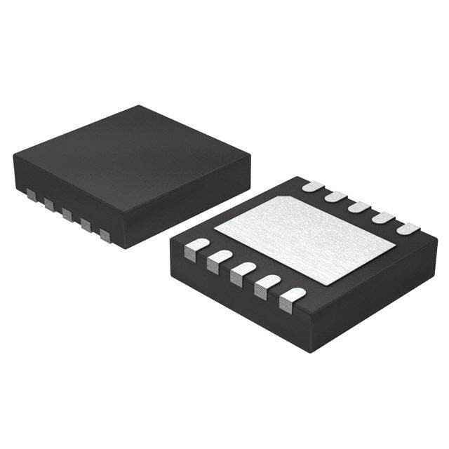
Product Sample & Technical Tools & Support & Folder Buy Documents Software Community TPS61310,TPS61311 SLVS978D–MARCH2010–REVISEDSEPTEMBER2016 TPS6131x 1.5-A Multiple LED Camera Flash and Video Light Driver 2 With I C Compatible Interface 1 Features 3 Description • OperationalModes: The TPS6131x family is an integrated solution with a 1 wide feature set for driving up to three LEDs for still- – VideoLightandFlashStrobe camera flash strobe and video-camera lighting – VoltageRegulatedConverter:3.8Vto5.7V applications. It is based on a high efficiency WithDownMode synchronous boost topology with combinable current sinks to drive up to three white LEDs in parallel. The – Standby:2µA(Typical) 2-MHz switching frequency allows the use of small • LEDV Measurement F and low-profile 2.2-µH inductors. To optimize overall • Power-SaveModeforImprovedEfficiencyatLow efficiency, the device operates with a low LED- OutputPower,Upto95%Efficiency feedback voltage and regulated output-voltage • I2CCompatibleInterfaceupto3.4Mbps adaptation. • DualWireCameraModuleInterface The device integrates a control scheme that automatically optimizes the LED current flash budget • ZeroLatencyTx-MaskingInput asafunctionofthebatteryvoltagecondition. • HardwareResetInput The TPS6131x not only operates as a regulated • PrivacyIndicatorLEDOutput current source, but also as a standard voltage boost • GPIOandPowerGoodOutput regulator. The device enters power-save mode • VariousSafeOperationandRobustHandling operation at light load currents to maintain high Features: efficiency over the entire load current range. These operating modes can be useful to supply other high – LEDTemperatureMonitoring power devices in the system (for example, a hands- – OpenandShortedLEDDetectionand freeaudioPA). Protection To simplify video light and flash synchronization with – IntegratedLEDSafetyTimer the camera module, the device offers a dedicated – AutomaticBatteryVoltageDroopMonitoring control interface (STRB0, STRB1) for zero latency andProtection LEDturnontime. – SmoothLEDCurrentRamp-UpandRamp- DeviceInformation(1) Down PARTNUMBER PACKAGE BODYSIZE(NOM) – UndervoltageLockout • TotalSolutionSizeofLessThan25mm2 TPS61310, DSBGA(20) 2.20mm×1.90mm TPS61311 • Availableina20-Pin NanoFree™DSBGA (1) For all available packages, see the orderable addendum at Package theendofthedatasheet. 2 Applications TypicalApplication • Single,Dual,orTripleWhiteLEDFlashSupplyfor L 2.2 mH CellPhonesandSmart-Phones SW SW VOUT • VideoLightingforDigitalVideoApplications AVIN • GeneralLightingApplications 2.55 .V5 tVo CI C10O mF D1 D2 4.7 mF • AudioAmplifierPowerSupply NRESET LED1 STRB0 LED2 STRB1 LED3 I2C I/F SSDCAL INDLED Privacy Indicator Tx-MASK TS GPIO/PG NTC AGND PGND AGND PGND Copyright © 2016,Texas Instruments Incorporated 1 An IMPORTANT NOTICE at the end of this data sheet addresses availability, warranty, changes, use in safety-critical applications, intellectualpropertymattersandotherimportantdisclaimers.PRODUCTIONDATA.
TPS61310,TPS61311 SLVS978D–MARCH2010–REVISEDSEPTEMBER2016 www.ti.com Table of Contents 1 Features.................................................................. 1 9.4 DeviceFunctionalModes........................................25 2 Applications........................................................... 1 9.5 RegisterMaps.........................................................30 3 Description............................................................. 1 10 ApplicationandImplementation........................ 38 4 RevisionHistory..................................................... 2 10.1 ApplicationInformation..........................................38 10.2 TypicalApplications..............................................38 5 DeviceComparisonTable..................................... 3 11 PowerSupplyRecommendations..................... 45 6 PinConfigurationandFunctions......................... 3 12 Layout................................................................... 45 7 Specifications......................................................... 4 12.1 LayoutGuidelines.................................................45 7.1 AbsoluteMaximumRatings......................................4 12.2 LayoutExample....................................................46 7.2 ESDRatings..............................................................4 12.3 ThermalConsiderations........................................46 7.3 RecommendedOperatingConditions.......................4 13 DeviceandDocumentationSupport................. 48 7.4 ThermalInformation..................................................5 7.5 ElectricalCharacteristics...........................................5 13.1 DocumentationSupport........................................48 7.6 I2CInterfaceTimingRequirements...........................7 13.2 RelatedLinks........................................................48 7.7 DissipationRatings...................................................8 13.3 ReceivingNotificationofDocumentationUpdates48 7.8 TypicalCharacteristics..............................................9 13.4 CommunityResources..........................................48 13.5 Trademarks...........................................................48 8 ParameterMeasurementInformation................13 13.6 ElectrostaticDischargeCaution............................48 9 DetailedDescription............................................ 14 13.7 Glossary................................................................48 9.1 Overview.................................................................14 14 Mechanical,Packaging,andOrderable 9.2 FunctionalBlockDiagram.......................................15 Information........................................................... 48 9.3 FeatureDescription.................................................16 4 Revision History NOTE:Pagenumbersforpreviousrevisionsmaydifferfrompagenumbersinthecurrentversion. ChangesfromRevisionC(November2012)toRevisionD Page • AddedDeviceInformationtable,ESDRatingstable,RecommendedOperatingConditionstable,ThermalInformation table,DeviceandDocumentationSupportsection,andMechanical,Packaging,andOrderableInformationsection...........1 • DeletedOrderingInformationtable;seePOAattheendofthedatasheet........................................................................... 1 ChangesfromRevisionB(September2011)toRevisionC Page • AddedrevisionletterCtoliteraturenumber........................................................................................................................... 1 • AddedTPS61311toorderingtable........................................................................................................................................ 3 • AddedCurrentLimitSettingforTPS61311.......................................................................................................................... 21 • AddedcurrentlimitsettingforTPS61311inregistermap.................................................................................................... 34 ChangesfromRevisionA(October2010)toRevisionB Page • ChangedV tomaxvaluefrom2.35Vto2.4V................................................................................................................ 5 UVLO • UpdatedLEDforwardvoltagecalibrationdescription.......................................................................................................... 24 • UpdatedSFTbitdescription................................................................................................................................................. 33 2 SubmitDocumentationFeedback Copyright©2010–2016,TexasInstrumentsIncorporated ProductFolderLinks:TPS61310 TPS61311
TPS61310,TPS61311 www.ti.com SLVS978D–MARCH2010–REVISEDSEPTEMBER2016 5 Device Comparison Table PACKAGE DEVICESPECIFICFEATURES(1) TPS61310 upto1750-mA(typical)inputvalleycurrent TPS61311 upto2480-mA(typical)inputvalleycurrent (1) Formoredetails,seeDetailedDescriptionandApplicationandImplementation. 6 Pin Configuration and Functions YFFPackage 20-PinDSBGA TopView A B C D E 4 AGND STRB0 TS GPIO/PG AVIN 3 AGND NRESET Tx-MASK STRB1 LED3 2 VOUT SCL SW PGND LED1 1 INDLED SDA SW PGND LED2 Not to scale PinFunctions PIN I/O DESCRIPTION NO. NAME A1 INDLED O ThispinprovidesaconstantcurrentsourcetodrivelowV LEDs.ConnecttoLEDanode. F A2 VOUT O Thisistheoutputvoltagepinoftheconverter. A3,A4 AGND — Analogground. B1 SDA I/O Serialinterfaceaddressanddataline.Thispinmustnotbeleftfloatingandmustbeterminated. B2 SCL I Serialinterfaceclockline.Thispinmustnotbeleftfloatingandmustbeterminated. Masterhardwareresetinput. NRESET=LOW:ThedeviceisforcedinshutdownmodeandtheI2CcontrolI/Fandallinternalcontrol B3 NRESET I registersarereset. NRESET=HIGH:ThedeviceisoperatingnormallyunderthecontroloftheI2Cinterface. LED1,LED2,andLED3enablelogicinput.Thispincanbeusedtoenableordisablethehigh-power LEDsconnectedtothedevice. B4 STRB0 I STRB0=LOW:LED1,LED2andLED3currentregulatorsareturnedoff. STRB0=HIGH:LED2,LED2andLED3currentregulatorsareactive.TheLEDcurrentlevel(videolight orflashcurrent)isdefinedaccordingtotheSTRB1logiclevel. Inductorconnection.DrainoftheinternalpowerMOSFET.Connecttotheswitchedsideoftheinductor. C1,C2 SW I/O SWishighimpedanceduringshutdown. RFPAsynchronizationcontrolinput.PullingthispinhighturnstheLEDfromflashtovideolight C3 Tx-MASK I operation,therebyreducingalmostinstantaneouslythepeakcurrentloadingfromthebattery. Copyright©2010–2016,TexasInstrumentsIncorporated SubmitDocumentationFeedback 3 ProductFolderLinks:TPS61310 TPS61311
TPS61310,TPS61311 SLVS978D–MARCH2010–REVISEDSEPTEMBER2016 www.ti.com PinFunctions(continued) PIN I/O DESCRIPTION NO. NAME NTCresistorconnection.ThispincanbeusedtomonitortheLEDtemperature.Connecta220-kΩNTC C4 TS I resistorfromtheTSinputtoground.Incasethisfunctionalityisnotdesired,theTSinputmustbetiedto AVINorleftfloating. D1,D2 PGND — Powerground.ConnecttoAGNDunderneathIC. LEDcurrentlevelselectioninput.Pullingthisinputhighdisablesthevideolightwatchdogtimer. D3 STRB1 I STRB1=LOW:flashmodeisenabled. STRB1=HIGH:videolightmodeisenabled. ThispincaneitherbeconfiguredasageneralpurposeI/Opin(GPIO)oreitherasanopen-drainora D4 GPIO/PG I/O push-pulloutputtosignalwhentheconvertersoutputvoltageiswithintheregulationlimits(PG).Per default,thepinisconfiguredasanopen-drainPowerGoodoutput. E1 LED2 I LEDreturninput(currentsinks).ThisfeedbackpinregulatestheLEDcurrentthroughtheinternalsense E2 LED1 I resistorbyregulatingthevoltageacrossit.ConnecttothecathodeofthewhiteLEDs. E3 LED3 I E4 AVIN I Thisistheinputvoltagepinofthedevice.Connectdirectlytotheinputbypasscapacitor. 7 Specifications 7.1 Absolute Maximum Ratings see (1) MIN MAX UNIT AVIN,VOUT,SW,LED1,LED2,LED3,SCL,SDA,STRB0,STRB1,NRESET, Voltage –0.3 7 V GPIO/PG,Tx-MASK,TS CurrentonGPIO/PG ±25 mA Powerdissipation Internallylimited Operatingambienttemperature,T (2) –40 85 °C A Maximumoperatingjunctiontemperature,T (2) 150 °C J Storagetemperature,T –65 150 °C stg (1) StressesbeyondthoselistedunderAbsoluteMaximumRatingsmaycausepermanentdamagetothedevice.Thesearestressratings only,whichdonotimplyfunctionaloperationofthedeviceattheseoranyotherconditionsbeyondthoseindicatedunderRecommended OperatingConditions.Exposuretoabsolute-maximum-ratedconditionsforextendedperiodsmayaffectdevicereliability. (2) Inapplicationswherehighpowerdissipationorpoorpackagethermalresistanceispresent,themaximumambienttemperaturemay havetobederated.Maximumambienttemperature[T ]isdependentonthemaximumoperatingjunctiontemperature[T ],the A(max) J(max) maximumpowerdissipationofthedeviceintheapplication[P ],andthejunction-to-ambientthermalresistanceofthepartinthe D(max) application(R ),asgivenby:T =T –(R ×P ) θJA A(max) J(max) θJA D(max) 7.2 ESD Ratings VALUE UNIT Human-bodymodel(HBM),perANSI/ESDA/JEDECJS-001(1) ±2000 V Electrostaticdischarge V (ESD) Charged-devicemodel(CDM),perJEDECspecificationJESD22-C101(2) ±500 (1) JEDECdocumentJEP155statesthat500-VHBMallowssafemanufacturingwithastandardESDcontrolprocess. (2) JEDECdocumentJEP157statesthat250-VCDMallowssafemanufacturingwithastandardESDcontrolprocess. 7.3 Recommended Operating Conditions overoperatingfree-airtemperaturerange(unlessotherwisenoted) MIN MAX UNIT T Operatingjunctiontemperature –40 125 °C J 4 SubmitDocumentationFeedback Copyright©2010–2016,TexasInstrumentsIncorporated ProductFolderLinks:TPS61310 TPS61311
TPS61310,TPS61311 www.ti.com SLVS978D–MARCH2010–REVISEDSEPTEMBER2016 7.4 Thermal Information TPS6131x THERMALMETRIC(1) YFF(DSBGA) UNIT 20PINS R Junction-to-ambientthermalresistance 71 °C/W θJA R Junction-to-case(top)thermalresistance 0.4 °C/W θJC(top) R Junction-to-boardthermalresistance 21 °C/W θJB ψ Junction-to-topcharacterizationparameter 1.9 °C/W JT ψ Junction-to-boardcharacterizationparameter 11.2 °C/W JB (1) Formoreinformationabouttraditionalandnewthermalmetrics,seetheSemiconductorandICPackageThermalMetricsapplication report. 7.5 Electrical Characteristics SpecificationappliesforV =3.6VoveranoperatingjunctiontemperatureT =–40°Cto125°C;seeFigure24(unless IN J otherwisenoted).TypicalvaluesareforT =25°C. J PARAMETER TESTCONDITIONS MIN TYP MAX UNIT SUPPLYCURRENT VIN Inputvoltage 2.5 5.5 V IOUT=0mA,devicenotswitching(PowerSafe 590 700 µA Mode),–40°C≤TJ≤85°C IQ OperatingquiescentcurrentintoAVIN IOUT(DC)=0mA,PWMoperationVOUT=4.95V, 11.3 mA voltageregulationmode ISD Shutdowncurrent –40°C≤TJ≤85°C 1 5 µA Undervoltagelockoutthreshold VUVLO (analogcircuitry) VINfalling 2.3 2.4 V OUTPUT Currentregulationmode VIN 5.5 Outputvoltage V Voltageregulationmode 3.825 5.7 VOUT Internalfeedbackvoltageaccuracy 2.5V≤VIN≤4.8V,–20°C≤TJ≤125°C,Boost –2% 2% mode,PWMvoltageregulation Power-savemoderipplevoltage IOUT=10mA 0.015×VOUT VP–P VOUTrising,0000≤OV[3:0]≤0100 4.5 4.65 4.8 Outputovervoltageprotection OVP VOUTrising,0101≤OV[3:0]≤1111 5.8 6 6.2 V Outputovervoltageprotectionhysteresis VOUTfalling 0.15 POWERSWITCH rDS(on) SwitchMOSFETON-resistance VOUT=VGS=3.6V 90 mΩ RectifierMOSFETON-resistance VOUT=VGS=3.6V 135 mΩ Ilkg(SW) LeakageintoSW VOUT=0V,SW=3.6V,–40°C≤TJ≤85°C 0.3 4 µA Ilim Rectifiervalleycurrentlimit(openloop) VPOWUMT=op4e.9r5atiVo,n–,2re0l°aCtiv≤eTtoJ≤se8le5c°Cte,dILIM –15% 15% OSCILLATOR fOSC Oscillatorfrequency 1.92 MHz fACC Oscillatorfrequency –10% 7% THERMALSHUTDOWN,HOTDIEDETECTOR Thermalshutdown(1) 140 160 °C Thermalshutdownhysteresis(1) 20 °C Hotdiedetectoraccuracy(1) –8 8 °C LEDCURRENTREGULATOR 0.4V≤VLED[1,3]≤2V, –10% 10% LED1andLED3currentaccuracy(2) 0mA≤ILED[1,3]≤100mA,TJ=85°C 0.4V≤VLED[1,3]≤2V, –7.5% 7.5% 100mA<ILED[1,3]≤400mA,TJ=85°C (1) Verifiedbycharacterization.Nottestedinproduction. (2) Verifiedbycharacterization.Nottestedinproduction. Copyright©2010–2016,TexasInstrumentsIncorporated SubmitDocumentationFeedback 5 ProductFolderLinks:TPS61310 TPS61311
TPS61310,TPS61311 SLVS978D–MARCH2010–REVISEDSEPTEMBER2016 www.ti.com Electrical Characteristics (continued) SpecificationappliesforV =3.6VoveranoperatingjunctiontemperatureT =–40°Cto125°C;seeFigure24(unless IN J otherwisenoted).TypicalvaluesareforT =25°C. J PARAMETER TESTCONDITIONS MIN TYP MAX UNIT 0.4V≤VLED2≤2V, –10% 10% LED2currentaccuracy(2) 0mA≤ILED2≤250mA,TJ=85°C 0.4V≤VLED2≤2V, –7.5% 7.5% 250mA≤ILED2≤800mA,TJ=85°C LED1andLED3currentmatching(2) –10% 10% LED1,LED2,andLED3currenttemperature 0.05 %/°C coefficient INDLEDcurrentaccuracy 1.5V≤(VIN–VINDLED)≤2.5V –20% 20% 2.6mA≤IINDLED≤15.8mA,TJ=25°C INDLEDcurrenttemperaturecoefficient 0.05 %/°C LED1,LED2,andLED3sensevoltage ILED[1,2,3]=full-scalecurrent 400 mV VDO VOUTdropoutvoltage IOUT=–15.8mA,TJ=25°C,devicenotswitching 250 mV LED1,LED2,andLED3inputleakagecurrent VLED[1,2,3]=VOUT=5V,–40°C≤TJ≤85°C 0.1 4 µA INDLEDinputleakagecurrent VINDLED=0V,–40°C≤TJ≤85°C 0.1 1 µA LEDTEMPERATUREMONITORING IO(TS) TemperatureSenseCurrentSource Thermistorbiascurrent 23.8 µA TSResistance(WarningTemperature) LEDWARNbit=1 39 44.5 50 kΩ TSResistance(HotTemperature) LEDHOTbit=1 12.5 14.5 16.5 kΩ SDA,SCL,GPIO/PG,Tx-MASK,STRB0,STRB1,NRESET V(IH) High-levelinputvoltage 1.2 V V(IL) Low-levelinputvoltage 0.4 V Low-leveloutputvoltage(SDA) IOL=8mA 0.3 V(OL) V Low-leveloutputvoltage(GPIO) DIR=1,IOL=5mA 0.3 V(OH) High-leveloutputvoltage(GPIO) DIR=1,GPIOTYPE=0,IOH=8mA VIN–0.4 V I(LKG) Logicinputleakagecurrent InputconnectedtoVINorGND,–40°C≤TJ≤85°C 0.01 0.1 µA STRB0,STRB1pulldownresistance STRB0,STRB1≤0.4V 400 RPD NRESETpulldownresistance NRESET≤0.4V 400 kΩ Tx-MASKpulldownresistance Tx-MASK≤0.4V 400 SDAInputCapacitance SDA=VINorGND 9 SCLInputCapacitance SCL=VINorGND 4 GPIO/PGInputCapacitance DIR=0,GPIO/PG=VINorGND 9 C(IN) STRB0InputCapacitance STRB0=VINorGND 3 pF STRB1InputCapacitance STRB1=VINorGND 3 NRESETInputCapacitance NRESET=VINorGND 3.5 Tx-MASKInputCapacitance Tx-MASK=VINorGND 4 TIMING tNRESET Resetpulsewidth 10 µs Fromshutdownintovideolightmode Start-uptime 1.2 ms ILED=150mA LEDcurrentsettlingtime(3)triggeredbyarising MODE_CTRL[1:0]=10,ILED2=from0mAto 500 µs edgeonSTRB0 950mA LEDcurrentsettlingtime(3)triggeredbyTx-MASK MODE_CTRL[1:0]=10,ILED2=from950mAto 20 µs 150mA (3) Settlingtimeto±15%ofthetargetvalue. 6 SubmitDocumentationFeedback Copyright©2010–2016,TexasInstrumentsIncorporated ProductFolderLinks:TPS61310 TPS61311
TPS61310,TPS61311 www.ti.com SLVS978D–MARCH2010–REVISEDSEPTEMBER2016 7.6 I2C Interface Timing Requirements see (1) MIN MAX UNIT Standardmode 100 kHz Fastmode 400 High-speedmode(writeoperation),C –100pFmax 3.4 B f SCLClockFrequency (SCL) High-speedmode(readoperation),C –100pFmax 3.4 B MHz High-speedmode(writeoperation),C –400pFmax 1.7 B High-speedmode(readoperation),C –400pFmax 1.7 B BusFreeTimeBetweenaSTOP Standardmode 4.7 t µs BUF andSTARTCondition Fastmode 1.3 Standardmode 4 µs HoldTime(Repeated)START t ,t Fastmode 600 HD STA Condition ns High-speedmode 160 Standardmode 4.7 µs Fastmode 1.3 t LOWPeriodoftheSCLClock LOW High-speedmode,C –100pFmax 160 B ns High-speedmode,C –400pFmax 320 B Standardmode 4 µs Fastmode 600 t HIGHPeriodoftheSCLClock HIGH High-speedmode,C –100pFmax 60 ns B High-speedmode,C –400pFmax 120 B Standardmode 4.7 µs SetupTimeforaRepeatedSTART t ,t Fastmode 600 SU STA Condition ns High-speedmode 160 Standardmode 250 t ,t DataSetupTime Fastmode 100 ns SU DAT High-speedmode 10 Standardmode 0 3.45 µs Fastmode 0 0.9 t ,t DataHoldTime HD DAT High-speedmode,C –100pFmax 0 70 B ns High-speedmode,C –400pFmax 0 150 B Standardmode 20+0.1×C 1000 B Fastmode 20+0.1×C 300 B t RiseTimeofSCLSignal ns RCL High-speedmode,C –100pFmax 10 40 B High-speedmode,C –400pFmax 20 80 B Standardmode 20+0.1×C 1000 B RiseTimeofSCLSignalAftera Fastmode 20+0.1×C 300 B t RepeatedSTARTConditionand ns RCL1 AfteranAcknowledgeBIT High-speedmode,CB–100pFmax 10 80 High-speedmode,C –400pFmax 20 160 B Standardmode 20+0.1×C 300 B Fastmode 20+0.1×C 300 B t FallTimeofSCLSignal ns FCL High-speedmode,C –100pFmax 10 40 B High-speedmode,C –400pFmax 20 80 B Standardmode 20+0.1×C 1000 B Fastmode 20+0.1×C 300 B t RiseTimeofSDASignal ns RDA High-speedmode,C –100pFmax 10 80 B High-speedmode,C –400pFmax 20 160 B (1) Specifiedbydesign.Nottestedinproduction. Copyright©2010–2016,TexasInstrumentsIncorporated SubmitDocumentationFeedback 7 ProductFolderLinks:TPS61310 TPS61311
TPS61310,TPS61311 SLVS978D–MARCH2010–REVISEDSEPTEMBER2016 www.ti.com I2C Interface Timing Requirements (continued) see(1) MIN MAX UNIT Standardmode 20+0.1×C 300 B Fastmode 20+0.1×C 300 B t FallTimeofSDASignal ns FDA High-speedmode,C –100pFmax 10 80 B High-speedmode,C –400pFmax 20 160 B Standardmode 4 µs t ,t SetupTimeforSTOPCondition Fastmode 600 SU STO ns High-speedmode 160 C CapacitiveLoadforSDAandSCL 400 pF B 7.7 Dissipation Ratings PACKAGE POWERRATING(T =25°C) DERATINGFACTORABOVET =25°C(1) A A YFF 1.4W 14mW/°C (1) MaximumpowerdissipationisafunctionofT ,R andT .Themaximumallowablepowerdissipationatanyallowableambient J(max) θJA A temperatureisP =(T –T )/R . D J(max) A θJA SDA tf tLOW tr tsu;DAT tf thd;STA tr tBUF SCL thd;STA tsu;STA tsu;STO S thd;DAT HIGH Sr P S Figure1. SerialInterfaceTimingForF/S-Mode Sr Sr P tfDA trDA SDAH thd;DAT tsu;STO tsu;STA thd;STA tsu;DAT SCLH tfCL trCL1 trCL trCL1 See Note A tHIGH tLOW tLOW tHIGH See Note A = MCS Current Source Pull-Up = R(P)Resistor Pull-Up Note A: First rising edge of the SCLH signal after Sr and after each acknowledge bit. Figure2. SerialInterfaceTimingForH/S-Mode 8 SubmitDocumentationFeedback Copyright©2010–2016,TexasInstrumentsIncorporated ProductFolderLinks:TPS61310 TPS61311
TPS61310,TPS61311 www.ti.com SLVS978D–MARCH2010–REVISEDSEPTEMBER2016 7.8 Typical Characteristics Table1.TableofGraphs CAPTION FIGURE LEDPowerEfficiency InputVoltage Figure3,Figure4 DCInputCurrent InputVoltage Figure5 LEDCurrent LEDPinHeadroomVoltage Figure6,Figure7 LEDCurrent LEDCurrentDigitalCode Figure8,Figure9,Figure10,Figure11 INDLEDCurrent INDLEDPinHeadroomVoltage Figure12 Efficiency OutputCurrent Figure13,Figure14 DCOutputVoltage LoadCurrent Figure15,Figure16 MaximumOutputCurrent InputVoltage Figure17 DCPrechargeCurrent DifferentialI/OVoltage Figure18,Figure19 SupplyCurrent InputVoltage Figure20 TemperatureDetectionThreshold Figure21,Figure22 JunctionTemperature PortVoltage Figure23 100 100 ILED1 =ILED3 = 350 mA 90 90 ILED2 = 600 mA % 80 % 80 N) - N) - ILED1 =ILED3 =50 mA PI 70 ILED2 = 75 mA PI 70 ILED2 = 100 mA LED/ 60 ILED2 = 100 mA LED/ 60 IILLEEDD12 == I1L5E0D m3 A= 75 mA P P cy ( 50 ILED2 = 150 mA cy ( 50 IILLEEDD12 == I2L0E0D m3 A= 100 mA en ILED2 = 225 mA en ILED1 =ILED3 = 250 mA Effici 40 Effici 40 ILEDI2L E= D415 0= mILAED3 = 250 mA er 30 er 30 ILED2 = 550 mA w w o o P 20 P 20 ED ILIM= 1750 mA, ED L 10 Tx-MASK = Low L 10 ILIM= 1750 mA, LED2 Channel Tx-MASK = Low 0 0 2.5 2.9 3.3 3.7 4.1 4.5 4.9 5.3 2.5 2.9 3.3 3.7 4.1 4.5 4.9 5.3 VI- Input Voltage - V VI- Input Voltage - V Figure3.LEDPowerEfficiencyvsInputVoltage Figure4.LEDPowerEfficiencyvsInputVoltage 2000 900 ILED2 = 800 mA ILED1 =ILED3 = 350 mA 1750 ILED2 = 600 mA 800 ILED2 = 700 mA 700 1500 mA A 600 ILED2 = 550 mA ent - 1250 nt - m 500 ILED2 = 450 mA ut Curr 1000 ILED1 =ILED3 = 250 mA 2 Curre 400 ILED2 = 350 mA C Inp 750 ILED2 = 550I LmEAD1 =ILED3 = 250 mA LED 300 ILED2 = 300 mA D 500 ILED2 = 450 mA 200 ILED1 =ILED3 = 250 mA ILED2 = 275 mA 250 ILIM= 1750 mA, 100 ILIM= 1750 mA Tx-MASK = Low 0 0 2.5 2.9 3.3 3.7 4.1 4.5 4.9 5.3 400 500 600 700 800 900 10001100120013001400 VI- Input Voltage - V LED2 Pin Headroom Voltage - mV Figure5.DCInputCurrentvsInputVoltage Figure6.LED2CurrentvsLED2PinHeadroomVoltage Copyright©2010–2016,TexasInstrumentsIncorporated SubmitDocumentationFeedback 9 ProductFolderLinks:TPS61310 TPS61311
TPS61310,TPS61311 SLVS978D–MARCH2010–REVISEDSEPTEMBER2016 www.ti.com Typical Characteristics (continued) 900 300 ILED1 =ILED3 = 400 mA 275 ILIM= 1750 mA 800 ILED1 =ILED3 = 350 mA 250 A 700 ILED1 =ILED3 = 300 mA 225 VIN= 2.5 V m A 1 + LED3 Current - 345600000000 ILED1 =ILED3 = 250 mA LED2 Current - m 111120257005050 VIN= 3.6 V VIN= 4.5 V D E L 200 75 50 100 ILIM= 1750 mA 25 0 0 400 500 600 700 800 900 10001100120013001400 0 25 50 75 100125150175200225250275300 LED1, LED3 Pin Headroom Voltage - mV LED2 Current Digital Code - mA Figure7.LED1+LED3Currentvs Figure8.LED2CurrentvsLED2CurrentDigitalCode LED1+LED3PinHeadroomVoltage 125 900 ILIM= 1750 mA 850 ILIM= 1750 mA VIN= 2.5 V 800 A 100 VIN= 3.6 V 750 m 700 D3 Current - 75 VIN= 2.5 V VIN= 4.5 V urrent - mA566505000 VIN= 3.6 V VIN= 4.5 V E C500 ED1, L LED2 440500 L 50 350 300 250 25 200 25 50 75 100 125 200 300 400 500 600 700 800 900 LED1, LED3 Current Digital Code - mA LED2 Current Digital Code - mA Figure9.LED1,LED3Currentvs Figure10.LED2CurrentvsLED2CurrentDigitalCode LED1,LED3CurrentDigitalCode 450 425 ILIM= 1750 mA VIN= 2.5 V 89 INDLED = 0011 TA= 85°C TA= 25°C TA= -40°C 400 7 A m 375 A Current - 332550 VIN= 3.6 V VIN= 4.5 V urrent - m 56 INDLED = 0010 TA= 85°C TA= 25°C D3 D C 4 ED1, LE 237050 INDLE 3 INDLED = 0001 TA= 85°C TA= 25°C TA= -40°C L 2 250 225 1 VIN= 3.6 V TA= -40°C 200 0 200 225 250 275 300 325 350 375 400 425 450 0.5 0.7 0.9 1.1 1.3 1.5 1.7 1.9 LED1, LED3 Current Digital Code - mA INDLED Pin Headroom Voltage - V Figure11.LED1,LED3Currentvs Figure12.INDLEDCurrentvs LED1,LED3CurrentDigitalCode INDLEDPinHeadroomVoltage 10 SubmitDocumentationFeedback Copyright©2010–2016,TexasInstrumentsIncorporated ProductFolderLinks:TPS61310 TPS61311
TPS61310,TPS61311 www.ti.com SLVS978D–MARCH2010–REVISEDSEPTEMBER2016 Typical Characteristics (continued) 100 100 VIN= 4.2 V VIN= 3.6 V 90 90 80 V = 3.6 V 80 VIN= 2.5 V VIN= 3 V VIN= 2.5 V IN Forced PWM Operation 70 VIN= 3 V 70 y - % 60 PFM/PWM Operation y - % 60 VIN= 4.2 V nc 50 nc 50 PFM/PWM Operation e e ci ci Effi 40 Effi 40 Forced PWM Operation 30 30 20 VOUT= 4.95 V 20 VOUT= 3.825 V ILIM= 1750 mA ILIM= 1750 mA 10 Voltage Mode Regulation 10 Voltage Mode Regulation 0 0 1 10 100 1000 10000 1 10 100 1000 10000 IO- Output Current - mA IO- Output Current - mA Figure13.EfficiencyvsOutputCurrent Figure14.EfficiencyvsOutputCurrent 5.2 4.016 Voltage Mode Regulation VOUT= 4.95 V, Voltage Mode Regulation 5.15 ILIM= 1750 mA 3.978 IOUT= 0 mA PFM/PWM Operation DC) - V 5.1 C) - V 3.94 age ( 5.05 ge (D 3.902 IOUT= 100 mA put Volt 5 VIN= 4.2 V ut Volta 3.863 Out 4.95 Forced PWM Operation utp 3.825 IOUT= 1000 mA - O - O V 4.9 O 3.787 V = 3.6 V V IN 4.85 3.749 VOUT= 3.825 V V = 2.5 V I = 1750 mA IN LIM 4.8 3.71 1 10 100 1000 10000 2.5 2.9 3.3 3.7 4.1 4.5 4.9 5.3 IO- Output Current - mA IO- Output Current - mA Figure15.DCOutputVoltagevsLoadCurrent Figure16.DCOutputVoltagevsLoadCurrent 1500 400 1400 Voltage Mode Regulation 1300 350 A 1200 VOUT= 4.95 V, A VIN= 3.6 V, TA= 25°C urrent (max) - m 11078910000000000 ILIM= 1250 mA VILOIMUT= =1 255.70 Vm,A arge Current - m 223050000 VIN= 4.2 V, TA= 25°C Output C 560000 C Pre-Ch 150 VIN= 2.5 V, TA= 25°C - 400 D 100 O I 300 200 50 100 0 0 2.5 2.9 3.3 3.7 4.1 4.5 4.9 5.3 0 0.6 1.2 1.8 2.4 3 3.6 4.2 V - Input Voltage - V Differential Input - Output Voltage - V I Figure17.MaximumOutputCurrentvsInputVoltage Figure18.DCPrechargeCurrentvs DifferentialI/OVoltage Copyright©2010–2016,TexasInstrumentsIncorporated SubmitDocumentationFeedback 11 ProductFolderLinks:TPS61310 TPS61311
TPS61310,TPS61311 SLVS978D–MARCH2010–REVISEDSEPTEMBER2016 www.ti.com Typical Characteristics (continued) 400 1500 1400 IOUT= 0 mA 350 VIN= 3.6 V, TA= -40°C ENPSM bit = ENVM bit = 1 1300 A 300 m A Current - 250 urrent -m 11210000 VOUT= 4.95 V, TA= 85°CVOUT= 5.7 V, TA= 25°C ge 200 y C 1000 Pre-Char 150 VIN= 3.6 V, TA= 85V°CIN= 3.6 V, TA= 25°C - SupplC 890000 DC 100 IC 700 VOUT= 4.95 V, VOTUAT== 32.58°2C5 V, 50 TA= -40°C VOUT= 4.95 V, 600 TA= 25°C 0 500 0 0.6 1.2 1.8 2.4 3 3.6 4.2 2.5 2.9 3.3 3.7 4.1 4.5 4.9 5.3 Differential Input - Output Voltage - V VI- Input Voltage - V Figure19.DCPrechargeCurrentvs Figure20.SupplyCurrentvsInputVoltage DifferentialI/OVoltage 26 28 24 VIN= 3.6 V 26 VIN= 3.6 V 22 24 20 22 ge - % 1168 ge - % 1280 mple Percenta 111024 mple Percenta 11110246 Sample Size = 76 Sa 8 Sample Size = 76 Sa 8 6 6 4 4 2 2 0 0 50 51 52 53 54 55 56 57 58 59 60 64 65 66 67 68 69 70 71 72 73 74 75 Temperature Detection (55°C Threshold) Temperature Detection (70°C Threshold) Figure21.TemperatureDetectionThreshold Figure22.TemperatureDetectionThreshold 200 175 IPORT= -100mA Tx-MASK Input 150 STRB1 Input C e - ° 125 ur erat 100 p m e 75 T n ctio 50 Jun 25 InpuPt oBrutffer - J T 0 100mA RT -25 VPO -50 -0.6 -0.55-0.5-0.45-0.4-0.35-0.3 -0.25-0.2 -0.15-0.1 Port Voltage - V Figure23.JunctionTemperaturevsPortVoltage 12 SubmitDocumentationFeedback Copyright©2010–2016,TexasInstrumentsIncorporated ProductFolderLinks:TPS61310 TPS61311
TPS61310,TPS61311 www.ti.com SLVS978D–MARCH2010–REVISEDSEPTEMBER2016 8 Parameter Measurement Information TPS61310 L SW SW VOUT 2.2 mH AVIN C O 2.5 V..5.5 V C I D1 D2 10 mF 4.7 mF NRESET LED 1 STRB0 LED 2 STRB1 LED 3 2 SCL I C I/F INDLED SDA Privacy Indicator Tx-MASK TS GPIO /PG NTC AGND PGND AGND PGND Copyright © 2016,Texas Instruments Incorporated L=2.2-µH C,C =10-µF,6.3-VX5R0603 I O NTC=220-kΩ Figure24. TPS61310TypicalApplicationCircuit Copyright©2010–2016,TexasInstrumentsIncorporated SubmitDocumentationFeedback 13 ProductFolderLinks:TPS61310 TPS61311
TPS61310,TPS61311 SLVS978D–MARCH2010–REVISEDSEPTEMBER2016 www.ti.com 9 Detailed Description 9.1 Overview TheTPS6131xfamilyisanintegratedsolutionwithawidefeaturesetfordrivinguptothreeLEDsforstill-camera flash and video-camera lighting applications. It employs a 2-MHz fixed on-time, PWM current-mode converter to generate the output voltage required to drive up to three high-power LEDs in parallel. The device integrates an NMOS-switch power stage and a synchronous PMOS rectifier. The device also implements a set of linear low- side current regulators to control the LED current when the battery voltage is higher than the diode forward voltage. The high-efficiency boost converter stage and LED forward voltage adoption ensure lowest device input current foragivenLEDoutputcurrent. A special circuit disconnects the load from the battery during shutdown of the converter. In conventional synchronous-rectifiercircuits,theback-gatediodeofthehigh-sidePMOSisforwardbiasedinshutdown,allowing current to flow from the battery to the output. The TPS6131x prevents this by disconnecting the cathode of the back-gatediodeofthehigh-sidePMOSfromthesourcewhentheregulatorisinshutdown. The TPS6131x device not only operates as a regulated current source, but also as a standard voltage-boost regulator featuring a power-save mode for improved efficiency at light loads. If the input voltage is higher than theprogrammedoutputvoltage,adownmodeisimplementedthatactssimilarlytoanLDO. The power stage is capable of supplying a maximum total current of roughly 1500 mA. The TPS6131x provides three constant-current sinks, capable of sinking up to 2 × 400 mA (LED1 and LED3) and 800 mA (LED2) in flash mode. Figure25. TPS6131xStates Special effort is taken for safe operation and robust system integration. The battery voltage can be monitored so that the flash current is not increased if the battery voltage drops by a programmable threshold. Internal timers limit the flash ON time to prevent potential camera-engine software errors, and a video light watchdog acts in a similar fashion. Multiple monitoring features (LED and die temperature, input voltage droop and so forth) keep thedeviceandLEDsoperatingproperly. TheTPS6131xintegratesanI2Ccompatibleinterfaceallowingtransfersupto3.4Mbpsforcontrollingthedevice, featuring low-speed mode, standard mode and high-speed mode compatible operation. Additionally, basic functions can be triggered by dedicated hardware input signals, such as STRB0 and STRB1 for triggering the flashorvideolightingwithzerolatency. 14 SubmitDocumentationFeedback Copyright©2010–2016,TexasInstrumentsIncorporated ProductFolderLinks:TPS61310 TPS61311
TPS61310,TPS61311 www.ti.com SLVS978D–MARCH2010–REVISEDSEPTEMBER2016 9.2 Functional Block Diagram AVIN SW Undervoltage Lockout Bias Supply Bandgap VREF= 1.238V COMPOAVRPATOR REF BCaockngtraotle VOUT Hot Die Indicator CVOBMATPADRRAOTOOPR AMEPRLRIOFIRER CoTnOtNrol SQ Digital VREF RQ Filter CONTROLLOGIC P COMPARATOR BATTERYDROOP THRESHOLD VOLTAGE REGULATION CURRENT REGULATION VLED Sense SENSE FB LED2 Max tONTimer ON/OFF SCL CURRENT SDA I2C I/F DAC CONTROL P SENSE FB LED1 LED Current Ramp Slew-Rate (STOP) Controller ON/OFF CURRENT Oscillator DAC CONTROL P STRB1 SENSE FB LED3 STRB0 Tx-MASK P NRESET Control Low-Side LED Current Regulator Logic 350kΩ AVIN INDLED INDC[1:0] AVIN High-Side LED Current Regulator 23µA TS WARNING VREF=1.05V HOT VREF=0.345V AGND PGND Copyright © 2016,Texas Instruments Incorporated Figure26. TPS6131x Copyright©2010–2016,TexasInstrumentsIncorporated SubmitDocumentationFeedback 15 ProductFolderLinks:TPS61310 TPS61311
TPS61310,TPS61311 SLVS978D–MARCH2010–REVISEDSEPTEMBER2016 www.ti.com Functional Block Diagram (continued) (GPIO Bit) Tx-MASK 350kW Port Direction (DIR) GPIO/PG CURRENTREGULATOR MODE–DC LIGHT/FLASHACTIVE MODE 0 MMOODDEE01==LHOIGWH Po(rPtTGy)pe STRB1 MODE 1 0 STRB0 1 1 350kW (GPIO Bit) SafetyTimerTrigger Edge Detect (STT) PWROK Start Flash/Timer (SFT) MODE0 DC Light MODE1 SafetyTimer (11.2s) 0:NORMALOPERATION 1:DISABLE CURRENTSINK Start LED1-3CURRENTCONTROL CLOCK 16-bit Prescaler SafetyTimer tPULSE 10::FDLCA LSIHG HCTUCRURRENRTENLETVLEELVEL Time-Out(TO) D(imDImMin)g (TVSiaTmlIueMer) LED1-3ON/OFF CONTROL Duty-Cycle Generator(5% ... 67%) 0:LED1-3OFF 1:DC LIGHTCURRENTLEVEL Copyright © 2016,Texas Instruments Incorporated Figure27. TimerBlock 9.3 Feature Description 9.3.1 PrivacyIndicator The privacy indicator functionality can be used to indicate when a person is being photographed or filmed. The TPS6131x device offers two options of privacy indication: A dedicated pin driving an additional privacy indicator LEDorusingthewhiteLEDswithpulsewidthmodulation. 9.3.1.1 DedicatedLEDPrivacyIndicator The TPS6131x device provides a high-side linear constant current source to drive low V LEDs. The LED current F is directly regulated off the battery and can be controlled through the INDC[3:0] bits, from 2.6 mA to 15.8 mA in 7 programablecurrentsteps. The device can drive two possible hardware configurations shown in Figure 28 and Figure 29. In Figure 28 the TPS6131xdevicedrivesaprivacyindicatorLEDtowardsground. 16 SubmitDocumentationFeedback Copyright©2010–2016,TexasInstrumentsIncorporated ProductFolderLinks:TPS61310 TPS61311
TPS61310,TPS61311 www.ti.com SLVS978D–MARCH2010–REVISEDSEPTEMBER2016 Feature Description (continued) VOUT VOUT C C OUT OUT LED1 TPS6131x LED1 TPS6131x LED2 LED2 LED3 LED3 INDLED INDLED Copyright © 2016,Texas Instruments Incorporated Copyright © 2016,Texas Instruments Incorporated Figure28.Configuration1 Figure29.Configuration2 The TPS6131x device also allows a path for driving a privacy indicator LED that is reverse biased to the white flash LED, see Figure 29. To do so, the output of the converter (VOUT) is pulled to ground thus allowing a reverse current to flow. This mode of operation is only possible when the converter’s power stage is in shutdown (MODE_CTRL[1:0]=00,ENVM=0). 9.3.1.2 WhiteLEDPrivacyIndicator The TPS6131x device features white LED drive capability at very low light intensity. To generate a reduced LED average current, the device employs a 30-kHz fixed-frequency PWM modulation scheme. The PWM timer uses the internal oscillator as reference clock, therefore the PWM modulating frequency shows the same accuracy as theinternalreferenceclock.OperationisshowninFigure27. The video light current is modulated with a duty cycle defined by the INDC[3:0] bits. The low light dimming mode can only be activated in the software-controlled video-light-only mode (MODE_CTRL[1:0] = 01, ENVM = 1), and applies to the LEDs selected through ENLED[3:1] bits. In this mode, the video light safety-timeout feature is disabled. PWM Dimming Steps 5%, 11%, 17%, 23%, 30%, 36%, 48%, 67% t1 IDCLIGHT ILED(DC)= IDCLIGHT x PWM Dimming Step 0 TPWM Figure30. PWMDimmingPrinciple 9.3.2 SafeOperationandProtectionFeatures 9.3.2.1 LEDTemperatureMonitoring(Finger-BurnProtection) The TPS6131x device optionally monitors the LED temperature. Critical temperatures are handled in two stages reflected by two bits: LEDWARN provides an early warning to the camera engine, LEDHOT immediately suspendstheflashoperation. The LED temperature is sensed by measuring the voltage drop of a negative-temperature-coefficient resistor connected between the TS and AGND pins. An internal current source provides the bias (approximately 24 µA) for the NTC, and the TS pin voltage is compared to internal thresholds (1.05 V and 0.345 V) to protect the LEDs againstoverheating.SeeNTCSelection. The temperature-monitoring blocks are explicitly active in video light or flash modes. In voltage-mode operation [MODE_CTRL[1:0]=11],thedeviceonlyactivatestheTSinputwhentheENTSbitissethigh. Copyright©2010–2016,TexasInstrumentsIncorporated SubmitDocumentationFeedback 17 ProductFolderLinks:TPS61310 TPS61311
TPS61310,TPS61311 SLVS978D–MARCH2010–REVISEDSEPTEMBER2016 www.ti.com Feature Description (continued) The LEDWARN and LEDHOT bits reflect the LED temperature. The LEDWARN bit is set when the voltage at the TS pin is lower than 1.05 V. This threshold corresponds to an LED warning temperature value; device operation is still permitted. While regulating LED current, video light or flash modes, the LEDHOT bit is latched when the voltage at the TS pin is lower than 0.345 V. This threshold corresponds to an excessive LED temperature value; deviceoperationisimmediatelysuspended,(MODE_CTRL[1:0]bitsarereset,andtheHOTDIE[1:0]bitsareset). 9.3.2.2 LEDFailureModes(OpenandShortDetection)andOvervoltageProtection The TPS6131x devices incorporate protection features to indicate if the connected LEDs are failing. These protections cover overvoltage conditions, which are caused by a failing LED showing open circuit behavior, as wellasshort-circuitconditionscausedbyafailingLEDorfurtherreasonscausingashort-circuitcondition.Ifsuch failure conditions occur, these are indicated by setting a failure detection flag. Furthermore, the maximum current drawnfromtheoutputislimitedandcanbeprogrammedbythecurrent-limitsetting. 9.3.2.2.1 LEDOpenCircuitDetectionandOvervoltageProtection IftheconnectedLED(s)failshowinganopencircuitbehaviororaredisconnected,theVOUToutputvoltagemust be limited to prevent the step-up converter from exceeding critical values. An overvoltage protection is implemented to avoid the output voltage exceeding critical values for the device and possibly for the system it is supplying. For this protection the TPS6131x output voltage is monitored internally. The TPS6131x device limits V according to the overvoltage protection settings (see Table 2). In this failure mode, V is either limited to OUT OUT 4.65 V (typical) or 6 V (typical) and the HIGH-POWER LED FAILURE (HPLF) flag is set. The OVP threshold dependsontheprogrammedoutputvoltage(OV). Table2.OVPSpecification OVPTHRESHOLD OPERATINGCONDITIONS 4.65Vtypical 0000≤OV[3:0]≤0100 6Vtypical 0101≤OV[3:0]≤1111 9.3.2.2.2 Short-CircuitProtection The TPS6131x devices incorporate double protection to protect the device and application circuit from short- circuitconditionsoccurringbetweenVOUTandthecurrentsinksLED1,LED2,andLED3. Ifashort-circuitconditionoccurswhiletheLEDsareoperated,thelowsidecurrentsinksLED1,LED2,LED3limit the maximum output current as programmed for the video-light mode or flash mode respectively. If a short-circuit condition occurs, the current sinks increase their input resistance to prevent excessive current to be drawn. Furthermore,theHIGH-POWERLEDFAILUREflag(HPLF)issettoindicatetheshortcircuitcondition.(HPLF)is triggered if the LED forward voltage drops below 1.23 V typically. The second protection is the current limit, whichgenerallylimitsthecurrentdrawnfromVOUT.SeeCurrentLimit. 9.3.2.3 LEDCurrentRamp-UpandRamp-Down To achieve smooth LED current waveforms and avoid excessive battery voltage drop, the TPS6131x device activelycontrolstheLEDcurrentramp-upandramp-downsequence. Table3.LEDCurrentRamp-UpandRamp-Down ControlvsOperatingMode LEDCURRENT OPERATINGMODE I =25mA STEP Ramp-up t =12µs RISE Slewrate×2.1mA/µs I =25mA STEP Ramp-down t =0.5µs FALL Slewrate×50mA/µs 18 SubmitDocumentationFeedback Copyright©2010–2016,TexasInstrumentsIncorporated ProductFolderLinks:TPS61310 TPS61311
TPS61310,TPS61311 www.ti.com SLVS978D–MARCH2010–REVISEDSEPTEMBER2016 LED CURRENT I STEP Time t t RISE FALL Figure31. LEDCurrentSlewRateControl 9.3.2.4 BatteryVoltageDroopMonitoringandProtection During a high-power flash strobe, the battery voltage usually drops by a few hundred millivolts. To prevent the battery voltage from collapsing too much, the TPS6131x devices integrates a battery voltage droop monitoring featuretoautomaticallylimittheflashcurrentifthebatteryvoltagedropsmorethanaprogrammablethreshold. ThebatteryvoltagedroopmonitoringfeaturecanbeenabledordisabledthroughtheENBATMONbit. At the very beginning of the flash strobe, the device measures the battery voltage and sets a minimum battery voltage threshold based on the tolerable droop (see REGISTER7 (address = 0x07) for BATDROOP[2:0] bits). While the LED current is increasing to the target flash current (see REGISTER1 (address = 0x01) and REGISTER2 (address = 0x02) for FC13[4:0] and FC2[5:0] bits), a comparator monitors the actual battery voltage and stops the ramp-up sequence when the droop exceeds the limit. See Functional Block Diagram and Figure32. ThebatteryvoltagedroopmonitorfeatureisautomaticallydisabledduringaTx-MASKevent. I LED Target Flash Current (950mA) Actual Flash Current (700mA) LED current is stopped from ramping further DC light VBAT Battery droop threshold maximum allowed exceeded Battery Droop (BATDROOP[2:0]) STRB0 Figure32. BatteryVoltageDroopMonitoringandLEDCurrentControlPrinciple(STRB1=0,Tx-Base=1) 9.3.2.5 UndervoltageLockout The undervoltage lockout circuit prevents the device from error conditions at low input voltages. It prevents the converter from turning on the switch MOSFET, or rectifier MOSFET for battery voltages below 2.3 V. The I2C compatibleinterfaceisfullyfunctionaldownto2.1-Vinputvoltage. 9.3.2.6 HotDieDetectionandThermalShutdown The TPS6131x device offers two levels of die temperature monitoring and protection, which are hot die detection and thermal shutdown functionality. The hot die detector (HOTDIE[1:0] bits) reflects the instantaneous junction temperature.Thisfunctionalityisalwaysenabledexceptwhenthedeviceisinshutdownmode. Copyright©2010–2016,TexasInstrumentsIncorporated SubmitDocumentationFeedback 19 ProductFolderLinks:TPS61310 TPS61311
TPS61310,TPS61311 SLVS978D–MARCH2010–REVISEDSEPTEMBER2016 www.ti.com The hot die detector monitors the junction temperature but does not shut down the device. It provides an early warning to the camera engine to avoid excessive power dissipation thus preventing from thermal shutdown duringthenexthigh-powerflashstrobe. As soon as the junction temperature T exceeds 160°C typical, the device goes into thermal shutdown. In this J mode, the power stage and the low-side current regulators are turned off, the HOTDIE[1:0] bits are set and can onlyberesetbyareadaccess.Inthevoltagemodeoperation(MODE_CTRL[1:0]=11orENVM=1),thedevice continues its operation when the junction temperature falls below 140°C typical again. In the current regulation mode,videolightorflashmodes,deviceoperationissuspended. Table4.DieTemperatureBits HOTDIE[1:0] JUNCTIONTEMPERATURE 00 <55°C 01 55°C≤T ≤70°C J 10 >70°C 11 Thermalshutdowntripped.Thebitisresetafterreadaccess 9.3.2.7 CurrentLimit The TPS6131x devices employ a programmable inductor current limit. This allows choosing inductors with different saturation current ratings. Furthermore, this provides protection against a shorted inductor, or if the inductancevaluedramaticallydrops.Thisprotectsthebatteryfromexcessivelyhighcurrentdrain. The current limit circuit employs a valley current sensing scheme. The detection threshold is user selectable throughtheILIMbit.TheILIMbitcanonlybesetbeforeenteringoperation,duringinitialshutdownstate. Figure 33 illustrates the inductor and rectifier current waveforms during current limit operation. The output current, IOUT, is the average of the rectifier ripple current waveform. When the load current is increased such thatthelowerpeakisabovethecurrentlimitthreshold,theofftimeislengthenedtoallowthecurrenttodecrease tothisthresholdbeforethenextONtimebegins(socalledfrequencyfoldbackmechanism). Both the output voltage and the switching frequency are reduced as the power stage of the device operates in a constant current mode. The maximum continuous output current (I ), before entering current limit operation, OUT(CL) canbedefinedas: 1 V D V - V I =(1 - D) ´ (I + DI )with DI = IN ´ and D » OUT IN OUT(CL) VALLEY L L 2 L f V OUT (1) The TPS6131x device also provides a negative current limit (≈ 300 mA) to prevent an excessive reverse inductor currentwhenthepowerstagesinkscurrentfromtheoutputintheforcedcontinuousconductionmode. DIL IPEAK Current Limit IVALLEY=ILIM Rectifier Threshold Current DIL IOUT(CL) IOUT(DC)(= ILED) Increased Load Current IIN(DC) f Inductor Current IIN(DC) DIL ΔIL= VIN×D L f Figure33. InductorandRectifierCurrentsinCurrentLimitOperation 20 SubmitDocumentationFeedback Copyright©2010–2016,TexasInstrumentsIncorporated ProductFolderLinks:TPS61310 TPS61311
TPS61310,TPS61311 www.ti.com SLVS978D–MARCH2010–REVISEDSEPTEMBER2016 Table5.InductorCurrentLimitOperation CURRENTLIMITSETTING ILIMBIT TPS61310 TPS61311 1250mA 1800mA Low 1750mA 2480mA High 9.3.2.8 FlashBlanking(Tx-Mask)forInstantaneousFlashCurrentReduction The TPS6131x devices offer a dedicated hardware signal input (Tx-Mask) that can be used to reduce the flash currenttotheprogrammedvideolightlevelinstantaneously. Thisfeaturecanbeusedtoreducetheoverallcurrentdrawnfromthebatteryifothersystemcomponentsrequire highenergysimultaneously,suchasduringaRFPAtransmissionpulse. TheTx-MASKfunctionhasnoinfluenceonthesafetytimerduration. FLASH LED CURRENT DC LIGHT Tx-MASK STRB0 Figure34. SynchronizedFlashWithBlankingPeriods(STRB1=0) 9.3.3 Start-UpSequence To avoid high inrush current during start-up, control the inrush current. When the device enables, the internal start-upcyclestartswiththefirststep,theprechargephase. During precharge, the rectifying switch is turned on until the output capacitor is either charged to a value close to the input voltage or ≈ 3.3 V, whichever occurs first. The rectifying switch is current limited during that phase. The currentlimitincreaseswithdecreasinginput-to-outputvoltagedifference.Thiscircuitalsolimitstheoutputcurrent underoutputshort-circuitconditions. After precharging the output capacitor, the device starts switching, and increases its current limit in three steps of typically 25 mA, 250 mA and full current limit (ILIM setting). The current limit transition from the first to the second step occurs after 1 ms of operation. Full current limit operation is set once the output voltage reaches its regulationlimits.Inthismode,theactivebalancingcircuitisdisabled. 9.3.4 NRESETInput:HardwareEnableorDisable The TPS6131x family features a hardware reset pin (NRESET). This reset pin allows the device to be disabled by an external controller without requiring an I2C write command. Under normal operation, the NRESET pin must be held high to prevent an unwanted reset. When the NRESET is driven low, the I2C control interface and all internalcontrolregistersareresettothedefaultstatesandthepartentersshutdownmode. Copyright©2010–2016,TexasInstrumentsIncorporated SubmitDocumentationFeedback 21 ProductFolderLinks:TPS61310 TPS61311
TPS61310,TPS61311 SLVS978D–MARCH2010–REVISEDSEPTEMBER2016 www.ti.com 9.3.5 SerialInterfaceDescription I2C™ is a 2-wire serial interface developed by Philips Semiconductor, now NXP Semiconductors [1]. The bus consists of a data line (SDA) and a clock line (SCL) with pullup structures. When the bus is idle, both SDA and SCL lines are pulled high. All the I2C compatible devices connect to the I2C bus through open drain I/O pins, SDA and SCL. A master device, usually a microcontroller or a digital signal processor, controls the bus. The master is responsible for generating the SCL signal and device addresses. The master also generates specific conditions that indicate the START and STOP of data transfer. A slave device receives or transmits data on the busundercontrolofthemasterdevice. The TPS6131x device works as a slave and supports these data transfer modes, as defined in the I2C Bus Specification: standard mode (100 kbps) and fast mode (400 kbps), and high-speed mode (3.4 Mbps). The interface adds flexibility to the power supply solution, enabling most functions to be programmed to new values depending on the instantaneous application requirements. Register contents remain intact as long as supply voltageremainsabove2.1V. Thedatatransferprotocolforstandardandfastmodesisexactlythesame,thereforetheyarereferredtoasF/S- modeinthisdocument.Theprotocolforhigh-speedmodeisdifferentfromF/S-mode,anditisreferredtoasH/S- mode. The TPS6131x device supports 7-bit addressing; 10-bit addressing and general call address are not supported.Thedevice7-bitaddressisdefinedas0110011. 9.3.5.1 F/S-ModeProtocol The master initiates data transfer by generating a start condition. The start condition is when a high-to-low transition occurs on the SDA line while SCL is high, as shown in Figure 35. All I2C-compatible devices must recognizeastartcondition. DATA CLK S P STARTCondition STOPCondition Figure35. StartandStopConditions The master then generates the SCL pulses, and transmits the 7-bit address and the read or write direction bit (R/W) on the SDA line. During all transmissions, the master checks for valid data. A valid data condition requires the SDA line to be stable during the entire high period of the clock pulse (see Figure 36). All devices recognize the address sent by the master and compare it to their internal fixed addresses. Only the slave device with a matching address generates an acknowledge (see Figure 37) by pulling the SDA line low during the entire high periodoftheninthSCLcycle.Upondetectingthisacknowledge,themasterknowsthatcommunicationlinkwitha slavehasbeenestablished. DATA CLK Data line Change stable; of data data valid allowed Figure36. BitTransferontheSerialInterface The master generates further SCL cycles to either transmit data to the slave (R/W bit 1) or receive data from the slave (R/W bit 0). In either case, the receiver must to acknowledge the data sent by the transmitter. So an acknowledge signal can either be generated by the master or by the slave, depending on which one is the receiver. 9-bit valid data sequences consisting of 8-bit data and 1-bit acknowledge can continue as long as necessary. 22 SubmitDocumentationFeedback Copyright©2010–2016,TexasInstrumentsIncorporated ProductFolderLinks:TPS61310 TPS61311
TPS61310,TPS61311 www.ti.com SLVS978D–MARCH2010–REVISEDSEPTEMBER2016 To signal the end of the data transfer, the master generates a stop condition by pulling the SDA line from low to high while the SCL line is high (see Figure 35). This releases the bus and stops the communication link with the addressed slave. All I2C compatible devices must recognize the stop condition. Upon the receipt of a stop condition, all devices know that the bus is released, and they wait for a start condition followed by a matching address. Attemptingtoreaddatafromregisteraddressesnotlistedinthissectionresultsin00hbeingreadout. Figure37. AcknowledgeontheI2CBus Figure38. BusProtocol 9.3.5.2 H/S-ModeProtocol The master generates a start condition followed by a valid serial byte containing HS master code 00001XXX. This transmission is made in F/S-mode at no more than 400 Kbps. No device is allowed to acknowledge the HS mastercode,butalldevicesmustrecognizeitandswitchtheirinternalsettingtosupport3.4-Mbpsoperation. Themasterthengeneratesarepeatedstartcondition(arepeatedstartconditionhasthesametimingasthestart condition). After this repeated start condition, the protocol is the same as F/S-mode, except that transmission speeds up to 3.4 Mbps are allowed. A stop condition ends the H/S-mode and switches all the internal settings of the slave devices to support the F/S-mode. Instead of using a stop condition, repeated start conditions should be usedtosecurethebusinH/S-mode. Attemptingtoreaddatafromregisteraddressesnotlistedinthissectionresultsin00hbeingreadout. 9.3.5.3 TPS6131xI2CUpdateSequence The TPS6131x requires a start condition, a valid I2C address, a register address byte, and a data byte for a single update. After the receipt of each byte, TPS6131x device acknowledges by pulling the SDA line low during thehighperiodofasingleclockpulse.AvalidI2CaddressselectstheTPS6131x.TPS6131xperformsanupdate onthefallingedgeoftheacknowledgesignalthatfollowstheLSBbyte. Copyright©2010–2016,TexasInstrumentsIncorporated SubmitDocumentationFeedback 23 ProductFolderLinks:TPS61310 TPS61311
TPS61310,TPS61311 SLVS978D–MARCH2010–REVISEDSEPTEMBER2016 www.ti.com 1 7 1 1 8 1 8 1 1 S SlaveAddress R/W A RegisterAddress A Data A P “0”Write From Master toTPS6131x A =Acknowledge S =STARTcondition Sr =REPEATED STARTcondition FromTPS6131x to Master P =STOPcondition Figure39. :Write DataTransferFormatinF/S-Mode 1 7 1 1 8 1 1 7 1 1 8 1 1 S SlaveAddress R/W A RegisterAddress A Sr SlaveAddress R/W A Data A P “0”Write “1”Read From Master toTPS6131x A =Acknowledge S =STARTcondition FromTPS6131x to Master Sr =REPEATED STARTcondition P =STOPcondition Figure40. ReadDataTransferFormatinF/S-Mode F/S Mode HS Mode F/S Mode 1 8 1 1 7 1 1 8 1 8 1 1 S HS-Master Code A Sr SlaveAddress R/W A RegisterAddress A Data A/A P DataTransferred (n x Bytes+Acknowledge) HS Mode Continues Sr SlaveAddress A =Acknowledge From Master toTPS6131x A =Acknowledge S =STARTcondition FromTPS6131x to Master Sr =REPEATED STARTcondition P =STOPcondition Figure41. DataTransferFormatinH/S-Mode 9.3.5.4 SlaveAddressByte MSB LSB X X X X X X A1 A0 TheslaveaddressbyteisthefirstbytereceivedfollowingtheSTARTconditionfromthemasterdevice. 9.3.5.5 RegisterAddressByte MSB LSB 0 0 0 0 00 D2 D1 D0 Following the successful acknowledgment of the slave address, the bus master sends a byte to the TPS6131x, whichcontainstheaddressoftheregistertobeaccessed. 9.3.6 LEDForwardVoltageCalibration High-power LEDs tend to exhibit a wide forward voltage distribution. The TPS6131x device integrates a self- calibration procedure that can be used to determine the actually LED forward voltage. The LED forward voltage in situ characterization can be performed at camera engine production test. This data can help to estimate more preciselytheactualLEDelectricalpowerversusflashcurrent. 24 SubmitDocumentationFeedback Copyright©2010–2016,TexasInstrumentsIncorporated ProductFolderLinks:TPS61310 TPS61311
TPS61310,TPS61311 www.ti.com SLVS978D–MARCH2010–REVISEDSEPTEMBER2016 This calibration procedure is meant to start at a minimum output voltage, and can be initiated by writing the SELFCAL bit (preferably with MODE_CTRL[1:0] = 00, ENVM = 0). The calibration procedure monitors the sense voltageacrossthelow-sidecurrentregulators(accordingtoENLED[3:1]bitssetting)andregisterstheworstcase LED, the LED featuring the largest forward voltage. The TPS6131x device automatically sweeps through its outputvoltagerangeandperformsashortdurationflashstrobeforeachstep(seeREGISTER1(address=0x01) andREGISTER2(address=0x02)forFC13[4:0]andFC2[5:0]bitssettings). Thesequenceisstoppedassoonasthedevicedetectsthateachofthelow-sidecurrentregulatorshaveenough headroom voltage (400 mV typical). The device returns the according output voltage in the register OV[3:0] and sets the SELFCAL bit. This bit is only being reset at the start or restart of a calibration cycle. In other words, when SELFCAL is asserted the output voltage register (OV[3:0]) returns the result of the last calibration sequence. Output Voltage,V OUT ESR x I ~200ms LED VBAT Feedback Sense Comparator Information Power Good,PG ~200ms LED Flash Current,I FLASH Feedback Sense Comparator Output V >400mV LED OV[3:0] 0000 0001 0010 0011 0100 0101 Self-Calibration, SELFCALbit(write) Self-Calibration, SELFCALbit(read) X Figure42. LEDForwardVoltageCalibrationPrinciple 9.4 Device Functional Modes 9.4.1 VideoLightandFlashStrobeOperation The TPS6131x devices drive one, two or three LEDs for video light and flash application. The video light and flash operation can either be triggered by an I2C software command or by means of dedicated, zero latency hardwaresignals. 9.4.1.1 LEDHardwareSetup The TPS6131x device uses LED forward-voltage sensing circuitry on LED1, LED2, and LED3 pins to optimize the power-stage boost ratio for maximum efficiency. Due to the nature of the sensing circuitry, TI does not recommend leaving any of the LED1, LED2, and LED3 pins unused if the operation is selected through ENLED[3:1] bits. Leaving LED1, LED2, and LED3 pins unconnected, while the respective ENLEDx bits have been set, forces the control loop into high gain, and eventually trips the output overvoltage protection. Figure 43 showstherecommendedLEDsetupforasingle,dualortriple-LEDapplication. Copyright©2010–2016,TexasInstrumentsIncorporated SubmitDocumentationFeedback 25 ProductFolderLinks:TPS61310 TPS61311
TPS61310,TPS61311 SLVS978D–MARCH2010–REVISEDSEPTEMBER2016 www.ti.com Device Functional Modes (continued) VOUT VOUT VOUT C C C TPS6131x OUT TPS6131x OUT TPS6131x OUT LED1 LED1 LED1 LED2 LED2 LED2 LED3 LED3 LED3 Single LED Dual LED Tripple LED Figure43. WhiteLEDHardwareSetupOptions The LED1, LED2, and LED3 inputs may be connected together to drive one or two LEDs at higher currents. Connecting the current sink inputs in parallel does not affect the internal operation of the TPS6131x. For best operation, TI recommends disabling the LED inputs that are not connected. (see the ENLED[3:1] bits description inREGISTER5(address=0x05)). The video light currents are individually programmed through the video light control bits DCL13[2:0] and DCL2[2:0] , the flash currents through FC2[5:0] and FC13[4:0] bits accordingly. If, for single or dual LED application as shown in Figure 43, current sinks are connected to each other and enabled, the resulting video or flashcurrentisthesumoftheprogrammedcurrents. 9.4.1.2 TriggeringVideoLightandFlash For most flexible system integration, the TPS6131x offers several options for activating the video light and flash. Depending on the settings of the MODE_CTRL[1:0] bits, the device can enter different modes of operation. It offers the option of triggering the video light and flash through hardware signals (STRB0, STRB1) or software I2C command. The flash-signal hardware trigger can be on the leading-edge, turning on for the programmed flash on time,orlevelsensitive,turningonforaslongasthesignalislogichigh. The TPS6131x flash timer is programmed through the STIM[2:0] and SELSTIM bits. If the flash is fired by a rising-edge trigger or by an I2C command, the timer defines the flash duration. If the flash is fired by a level- sensitive trigger, the timer defines the maximum flash ON duration, and overrides the hardware signal if the programmedon-timeisexceeded. For video lighting, a watchdog timer is implemented; this must be refreshed within 13 seconds. This function can bedisabled,asdescribedinTable6. Table6.ModeOperationsforVideoLightandFlash MODE_CTRLSETTING DESCRIPTION TheSTRB0,STRB1inputsaredisabled.ThedeviceregulatestheLEDcurrentinvideolightmode (DCLCbits)regardlessoftheSTRB0,STRB1inputsandtheSTART_FLASH/TIMER(SFT)bit.Toavoid MODE_CTRL[1:0]=01 deviceshutdownbecauseofthevideolightsafetytimeout,MODE_CTRL[1:0]mustberefreshedwithin lessthan13seconds(STRB1=0).Thevideolightwatchdogtimercanbedisabledbypullingthe STRB1signalhigh. TheSTRB0,STRB1inputsareenabled.Theflashpulsecanbetriggeredbythesesynchronization signals,orbyasoftwarecommand(START_FLASH/TIMER(SFT)bit).TheLEDsareenabledor MODE_CTRL[1:0]=10 disabledaccordingtotheSTRB0,STRB1input.Theflashsafetytimerisactivated,andthevideolight watchdogtimerisdisabled. The dual-wire camera-module interface STRB0 and STRB1 inputs are used for selecting the video light (STRB1 = 1) or flash (STRB1 = 0) mode. The STRB0 signal then triggers the video light or flash, depending on the state of STRB1. The STT bit defines if the flash trigger is level sensitive (STT = 0), or fired on the rising edge (STT=1). 26 SubmitDocumentationFeedback Copyright©2010–2016,TexasInstrumentsIncorporated ProductFolderLinks:TPS61310 TPS61311
TPS61310,TPS61311 www.ti.com SLVS978D–MARCH2010–REVISEDSEPTEMBER2016 9.4.1.3 Level-SensitiveFlashTrigger(STT=0) In this mode, the high-power LEDs are driven at the flash current level and the safety timer (STIM) is running. ThemaximumdurationoftheflashpulseisdefinedintheSTIM[2:0]register. The safety timer is triggered on rising edge and stopped by a negative logic on the synchronization source (STRB0,STRB1=0)orbyatimeoutevent(TObit). AFASSISTLIGHT STROBE STRB0 STRB1 DURATION < STIM TIMER LED CONTROL LED OFF LED OFF LED OFF DC LIGHT FLASH Figure44. HardwareSynchronizedVideoLightandFlashStrobe 9.4.1.4 Rising-EdgeFlashTrigger(STT=1) In this mode, the high-power LEDs are driven at the flash current level and the safety timer (STIM) is running. ThedurationoftheflashpulseisdefinedintheSTIM[2:0]register. Theflashstrobeisstartedeitherbyarisingedgeonthesynchronizationsource(STRB0=1,STRB1=0)orbya positive transition on the START-FLASH/TIMER (SFT) bit (STRB0 = 1, STRB1 = 0). Once running, the timer ignoresallkindoftriggeringsignalsandonlystopsafteratimeout(TO).START-FLASH/TIMER(SFT)bitisbeing resetbythetimeout(TO)signal. AFASSISTLIGHT STROBE STRB0 STRB1 DURATION = STIM TIMER LED CONTROL LED OFF LED OFF LED OFF DC LIGHT FLASH Figure45. EdgeSensitiveTimer(SingleTriggerEvent) 9.4.2 VoltageMode In this mode, the TPS6131x operates as a standard voltage-boost regulator, featuring power-save mode for improved efficiency under light loads. The voltage-mode operation is enabled by software control by setting the mode-control bit MODE_CTRL[1:0] = 11. The device regulates a constant output voltage according to the OV[3:0] bit settings (from 3.825 V to 5.7 V in 125-mV steps). In voltage mode, the LED current sinks LED1, LED2,andLED3areturnedoff. The TPS6131x integrates a software control bit (ENVM bit) that can be used to force the converter to run in voltage mode. This enables the converter to operate at a fixed programmed output voltage (according to the OV[3:0]settings)whileoperatingtheLEDs. Table7providesanoverviewofthedifferentvoltagemodevariations. Copyright©2010–2016,TexasInstrumentsIncorporated SubmitDocumentationFeedback 27 ProductFolderLinks:TPS61310 TPS61311
TPS61310,TPS61311 SLVS978D–MARCH2010–REVISEDSEPTEMBER2016 www.ti.com Table7.VoltageModeDescription INTERNALREGISTER ENVM OPERATINGMODES SETTINGSMODE_CTRL[1:0] BIT 11 0 LEDsareturnedoffandtheconverteroperateinvoltage-regulationmode(VM);theoutput 00 1 voltageissetthroughregisterOV[3:0]. Theconverteroperatesinvoltage-regulationmode(VM);theoutputvoltageissetthroughthe registerOV[3:0].TheLEDsareturnedonforvideolightoperationandtheenergyisbeing 01 1 directlytransferredfromthebatterytotheoutput.TheLEDcurrentsareregulatedbythemeans ofthelow-sidecurrentsinks. Theconverteroperatesinthevoltage-regulationmode(VM);theoutputvoltageissetthrough 10 1 theregisterOV[3:0].TheLEDcurrentsareregulatedbythelow-sidecurrentsinks.TheLEDs arereadyforflashoperation. LEDsareturnedoffandtheconverteroperatesinthevoltageregulationmode(VM);theoutput 11 1 voltageissetthroughtheregisterOV[3:0]. 9.4.2.1 DownModeinVoltageModeOperation In general, a boost converter only regulates output voltages which are higher than the input voltage. The TPS6131x can regulate 4.2 V at the output with an input voltage as high as 5.5 V. To control these applications properly,adown-conversionmodeisimplemented. In voltage-regulation mode, if the input voltage reaches or exceeds the output voltage, the converter changes to down-conversion mode. In this mode, the control circuit changes the behavior of the rectifying PMOS. It sets the voltage drop across the PMOS as high as required to regulate the output voltage. This increases the power losses in the converter, and must be considered for thermal design. The down-conversion mode is automatically turnedoffassoonastheinputvoltagefallstoapproximately200mVbelowtheoutputvoltage. For proper operation in down-conversion mode the output voltage must not be programmed higher than approximately5.3V.TakecarenottoviolatetheabsolutemaximumratingsattheSWpins. 9.4.2.2 PowerGoodIndication The TPS6131x integrates a Power Good circuit that is activated when the device operates in voltage-regulation mode (MODE_CTRL[1:0] = 11 or ENVM = 1). In shutdown mode (MODE_CTRL[1:0] = 00, ENVM = 0), the GPIO/PGpinstateisdefinedbelow,accordingtotheGPIOTYPEbit: Table8.GPIO/PGStateinShutdown GPIOTYPE GPIO/PGSHUTDOWNSTATE 0 Resetorpulledtoground 1 Open-drain Depending on the GPIO/PG output stage type selection, push-pull or open-drain, the polarity of the Power Good output signal (PG) can be inverted or not. The Power Good software bit and hardware signal polarity is defined below: Table9.PowerGoodSignalPolarity GPIOTYPE PGBIT GPIO/PGOUTPUTPORT COMMENTS 0 0 0:push-pulloutput Outputisactive-high 1 1 0 Open-drain 1:open-drainoutput Outputisactive-low 1 Low 28 SubmitDocumentationFeedback Copyright©2010–2016,TexasInstrumentsIncorporated ProductFolderLinks:TPS61310 TPS61311
TPS61310,TPS61311 www.ti.com SLVS978D–MARCH2010–REVISEDSEPTEMBER2016 ThePowerGoodsignalistruewhentheoutputvoltageisfrom –1.5%to2.5%ofitsnominalvalue.Conversely,it isfalsewhenthevoltage-modeoperationissuspended(MODE_CTRL[1:0] ≠ 11andENVM=0). Forced PWM mode operation Output Voltage Voltage Mode Request Down Regulation Nom.Voltage 1.025VOUT(NOM) Output Voltage,VOUT VOUT(NOM) Start-up phase 0.985VOUT(NOM) Output Voltage Power Good Bit,(PG) Up Regulation Power Good Output, Forced PWM mode operation Hi-Z Hi-Z GPIO/PG (PG)Bit Figure46. PowerGoodOperation(DIR=1,GPIOTYPE=1) The TPS6131x device uses a control architecture that recycles excess energy that might be stored in the output capacitor. By reversing the operation of the boost power stage, the converter is capable of transferring energy from its output back into the input source. In this case, the Power Good signal is deasserted while the output voltageisdecreasingtowardsitstargetvalue,theclosestfitvoltagetheconvertercansupport. 9.4.3 Power-SaveModeOperation,Efficiency The TPS6131x integrates a power-save mode to improve efficiency under light loads. In power-save mode the converter only operates when the output voltage trips below a set threshold voltage. It ramps up the output voltage with one to several pulses and returns to power-save mode once the output voltage exceeds the set thresholdvoltage. Output Voltage PFM mode at light load PFM ripple about0.015x V OUT 1.013x V OUTNOM. V OUTNOM. PWM mode at heavy load Figure47. OperationinPFMModeandTransfertoPWMMode The power-save mode can be enabled and disabled through the ENPSM bit. In down conversion mode, power- savemodeisalwaysactiveandthedevicecannotbeforcedintofixedfrequencyoperationatlightloads. The LED sense voltage has a direct effect on converter efficiency. Because the voltage across the low-side current regulator does not contribute to the output power (LED brightness), the lower the sense voltage the highertheefficiencyis. Theintegratedcurrentcontrolloopautomaticallyselectstheminimumboostratiotomaintainregulationbasedon the LED forward voltage and current requirements. The low-side current regulators drop the voltage difference between the input voltage and the LEDs forward voltage (V < V ). When running in boost mode (V > V ), the voltage present at the LED1, LED2, and LED3 F(LED) IN F(LED) IN pins of the low-side current regulators is typically 400 mV, leading to high power conversion efficiency. Depending on the input voltage and the LEDs forward voltage characteristic the converter efficiency is approximately75%to90%. Copyright©2010–2016,TexasInstrumentsIncorporated SubmitDocumentationFeedback 29 ProductFolderLinks:TPS61310 TPS61311
TPS61310,TPS61311 SLVS978D–MARCH2010–REVISEDSEPTEMBER2016 www.ti.com 9.4.4 Shutdown Writing 00 to MODE_CTRL[1:0] bits forces the device into shutdown. The shutdown state can only be entered whenthevoltageregulation(ENVM=0)andlightmodesarebothturnedoff. Intheshutdownstate: • Theregulatorstopsswitching. • Thehigh-sidePMOSdisconnectstheloadfromtheinput. • TheLEDxpinsarehighimpedancethuseliminatinganyDCconductionpath. • TheTPS6131xdeviceactivelydischargestheoutputcapacitorwhenitturnsoff. 9.5 Register Maps 9.5.1 REGISTER0(address=0x00) Figure48. REGISTER0Fields D7 D6 D5 D4 D3 D2 D1 D0 RESET — DCLC13[2:0] DCLC2[2:0] R/W-0 R/W-0 R/W-0 R/W-0 R/W-1 R/W-0 R/W-1 R/W-0 LEGEND:R/W=Read/Write;R=Readonly;-n=valueafterreset Table10.REGISTER0FieldDescriptions BIT DESCRIPTION RegisterResetbit RESET 0:Normaloperation. 1:Defaultvaluesaresettoallinternalregisters. VideoLightCurrentControlbits(LED1andLED3) 000:0mA(1)(2) 001:25mA 010:50mA DCLC13[2:0] 011:75mA 100:100mA 101:125mA 110:150mA 111:175mA VideoLightCurrentControlbits(LED2) 000:0mA(1)(2) 001:25mA 010:50mA DCLC2[2:0] 011:75mA 100:100mA 101:125mA 110:150mA,225mAcurrentlevelcanbeactivatedsimultaneouslywithTx-MASK=1 111:175mA,325mAcurrentlevelcanbeactivatedsimultaneouslywithTx-MASK=1 (1) LEDsareoff,V setaccordingtoOV[3:0]. OUT (2) WhenDCLC2[2:0]andDCLC13[2:0]arebothreset,thedeviceoperatesinvoltageregulationmode.Theoutputvoltageissetaccording toOV[3:0]. 30 SubmitDocumentationFeedback Copyright©2010–2016,TexasInstrumentsIncorporated ProductFolderLinks:TPS61310 TPS61311
TPS61310,TPS61311 www.ti.com SLVS978D–MARCH2010–REVISEDSEPTEMBER2016 9.5.2 REGISTER1(address=0x01) Figure49. REGISTER1Fields D7 D6 D5 D4 D3 D2 D1 D0 MODE_CTRL[1:0] FC2[5:0] R/W-0 R/W-0 R/W-0 R/W-1 R/W-0 R/W-0 R/W-0 R/W-0 LEGEND:R/W=Read/Write;R=Readonly;-n=valueafterreset Table11.REGISTER1FieldDescriptions BIT DESCRIPTION ModeControlbits 00:Deviceinshutdownmode. 01:Deviceoperatesinvideolightmode. 10:Deviceoperatesinflashmode. MODE_CTRL[1:0] 11:Deviceoperatesasconstantvoltagesource. Toavoiddeviceshutdownbyvideolightsafetytimeout,MODE_CTRL[1:0]bitsmustberefreshedwithinlessthan 13s. WritingtoREGISTER1[7:6]automaticallyupdatesREGISTER2[7:6]. FlashCurrentControlbits(LED2) 000000:0mA(1)(2) 000001:25mA 000010:50mA 000011:75mA 000100:100mA 000101:125mA 000110:150mA 000111:175mA 001000:200mA 001001:225mA 001010:250mA 001011:275mA 001100:300mA 001101:325mA 001110:350mA 001111:375mA FC2[5:0] 010000:400mA 010001:425mA 010010:450mA 010011:475mA 010100:500mA 010101:525mA 010110:550mA 010111:575mA 011000:600mA 011001:625mA 011010:650mA 011011:675mA 011100:700mA 011101:725mA 011110:750mA 011111:775mA 100000to111111:800mA (1) LEDsareoff,V setaccordingtoOV[3:0]. OUT (2) WhenFC13[4:0]andFC2[5:0]arebothreset,thedeviceoperatesinvoltageregulationmode.Theoutputvoltageissetaccordingto OV[3:0]. Copyright©2010–2016,TexasInstrumentsIncorporated SubmitDocumentationFeedback 31 ProductFolderLinks:TPS61310 TPS61311
TPS61310,TPS61311 SLVS978D–MARCH2010–REVISEDSEPTEMBER2016 www.ti.com 9.5.3 REGISTER2(address=0x02) Figure50. REGISTER2Fields D7 D6 D5 D4 D3 D2 D1 D0 MODE_CTRL[1:0] ENVM FC13[4:0] R/W-0 R/W-0 R/W-0 R/W-0 R/W-1 R/W-0 R/W-0 R/W-0 LEGEND:R/W=Read/Write;R=Readonly;-n=valueafterreset Table12.REGISTER2FieldDescriptions BIT DESCRIPTION ModeControlbits 00:Deviceinshutdownmode. 01:Deviceoperatesinvideolightmode. 10:Deviceoperatesinflashmode. MODE_CTRL[1:0] 11:Deviceoperatesasconstantvoltagesource. Toavoiddeviceshutdownbyvideolightsafetytimeout,MODE_CTRL[1:0]bitsmustberefreshedwithinlessthan 13s. WritingtoREGISTER2[6:5]automaticallyupdatesREGISTER1[6:5]. EnableVoltageModebit. 0:Normaloperation. ENVM 1:Forcesthedeviceintoaconstantvoltagesource. Inreadmode,theENVMbitisautomaticallyupdatedtoreflectthelogicstateoftheENVMinputpin. FlashCurrentControlbits(LED1andLED3) 00000:0mA(1)(2) 00001:25mA 00010:50mA 00011:75mA 00100:100mA 00101:125mA 00110:150mA 00111:175mA FC13[4:0] 01000:200mA 01001:225mA 01010:250mA 01011:275mA 01100:300mA 01101:325mA 01110:350mA 01111:375mA 10000to11111:400mA (1) LEDsareoff,V setaccordingtoOV[3:0]. OUT (2) WhenFC13[4:0]andFC2[5:0]arebothreset,thedeviceoperatesinvoltageregulationmode.Theoutputvoltageissetaccordingto OV[3:0]. 32 SubmitDocumentationFeedback Copyright©2010–2016,TexasInstrumentsIncorporated ProductFolderLinks:TPS61310 TPS61311
TPS61310,TPS61311 www.ti.com SLVS978D–MARCH2010–REVISEDSEPTEMBER2016 9.5.4 REGISTER3(address=0x03) Figure51. REGISTER3Fields D7 D6 D5 D4 D3 D2 D1 D0 SELSTIM(W) STIM[2:0] HPFL STT SFT Tx-MASK TO(R) R/W-1 R/W-1 R/W-0 R-0 R-0 R/W-0 R/W-0 R/W-1 LEGEND:R/W=Read/Write;R=Readonly;-n=valueafterreset Table13.REGISTER3FieldDescriptions BIT DESCRIPTION SafetyTimerbits STIM[2:0] RANGE0 RANGE1 000 68.2ms 5.3ms 001 102.2ms 10.7ms STIM[2:0] 010 136.3ms 16ms 011 170.4ms 21.3ms 100 204.5ms 26.6ms 101 340.8ms 32ms 110 579.3ms 37.3ms 111 852ms 71.5ms High-PowerLEDFailureflag 0:ProperLEDoperation. HPFL 1:LEDfailed(openorshorted). High-powerLEDfailureflagisresetafterreadout SafetyTimerSelectionRange(WriteOnly) SELSTIM 0:Safetytimerrange0. 1:Safetytimerrange1. Time-OutFlag(ReadOnly) TO 0:Notime-outeventoccurred. 1:Time-outeventoccurred.Time-outflagisresetatrestartofthesafetytimer. SafetyTimerTriggerbit 0:LEDsafetytimerislevelsensitive. STT 1:LEDsafetytimerisrisingedgesensitive. ThisbitisonlyvalidforMODE_CTRL[1:0]=10. Start/FlashTimerbit Inwritemode,thisbitinitiatesaflashstrobesequence.NoticethatthisbitisonlyactivewhenSTRB0inputishigh. 0:Nochangeinthehigh-powerLEDcurrent. SFT 1:High-powerLEDcurrentrampstotheflashcurrentlevel. Inreadmode,thisbitindicatesthehigh-powerLEDstatus. 0:High-powerLEDsareidle. 1:Ongoinghigh-powerLEDflashstrobe. FlashBlankingControlbit Inwritemode,thisbitenablesanddisablestheflashblankingandLEDcurrentreductionfunction. 0:Flashblankingdisabled. 1:LEDcurrentisreducedtovideolightlevelwhenTx-MASKinputishigh. Tx-MASK Inreadmode,thisflagindicateswhetherornottheflashmaskinginputisactivated.Tx-MASKflagisresetafter readoutoftheflag. 0:Noflashblankingeventoccurred. 1:Tx-MASKinputtriggered. Copyright©2010–2016,TexasInstrumentsIncorporated SubmitDocumentationFeedback 33 ProductFolderLinks:TPS61310 TPS61311
TPS61310,TPS61311 SLVS978D–MARCH2010–REVISEDSEPTEMBER2016 www.ti.com 9.5.5 REGISTER4(address=0x04) Figure52. REGISTER4Fields D7 D6 D5 D4 D3 D2 D1 D0 PG HOTDIE[1:0] ILIM INDC[3:0] R/W-0 R-0 R-0 R/W-0 R/W-0 R/W-0 R/W-0 R/W-0 LEGEND:R/W=Read/Write;R=Readonly;-n=valueafterreset Table14.REGISTER4FieldDescriptions Bit Description PowerGoodbit Inwritemode,thisbitselectsthefunctionalityoftheGPIO/PGoutput. 0:PGsignalisroutedtotheGPIOport. PG 1:GPIOPORTVALUEbitisroutedtotheGPIOport. Inreadmode,thisbitindicatestheoutputvoltageconditions. 0:Theconverterisnotoperatingwithinthevoltageregulationlimits. 1:Theoutputvoltageiswithinitsnominalvalue. InstantaneousDieTemperaturebits 00:T <55°C J HOTDIE[1:0] 01:55°C<T <70°C J 10:T >70°C J 11:Thermalshutdowntripped.Indicatorflagisresetafterreadout. InductorValleyCurrentLimitbit TheILIMbitcanonlybesetbeforethedeviceentersoperation,duringinitialshutdownstate. VALLEYCURRENTLIMITSETTING ILIMBITSETTING ILIM TPS61310 TPS61311 1250mA 1800mA Low 1750mA 2480mA High IndicatorLightControlbits INDC[3:0]:PRIVACYINDICATORINDLEDCHANNEL INDC[3:0]:PRIVACYINDICATORLED1,LED2,and _ LED3CHANNELS(2) 0000:Privacyindicatorturnedoff 1000:5%PWMdimmingratio 0001:INDLEDcurrent=2.6mA(1) 1001:11%PWMdimmingratio INDC[3:0] 0010:INDLEDcurrent=5.2mA(1) 1010:17%PWMdimmingratio 0011:INDLEDcurrent=7.9mA(1) 1011:23%PWMdimmingratio 0100:Privacyindicatorturnedoff 1100:30%PWMdimmingratio 0101:INDLEDcurrent=5.2mA(1) 1101:36%PWMdimmingratio 0110:INDLEDcurrent=10.4mA(1) 1110:48%PWMdimmingratio 0111:INDLEDcurrent=15.8mA (1) 1111:67%PWMdimmingratio (1) Theoutputnode(VOUT)isinternallypulledtoground. (2) ThismodeofoperationcanonlybeactivatedforMODE_CTRL[1:0]=01andENVM=1. 34 SubmitDocumentationFeedback Copyright©2010–2016,TexasInstrumentsIncorporated ProductFolderLinks:TPS61310 TPS61311
TPS61310,TPS61311 www.ti.com SLVS978D–MARCH2010–REVISEDSEPTEMBER2016 9.5.6 REGISTER5(address=0x05) Figure53. REGISTER5Fields D7 D6 D5 D4 D3 D2 D1 D0 DIR(W) SELFCAL ENPSM GPIO GPIOTYPE ENLED3 ENLED2 ENLED1 STSTRB1(R) R/W-0 R/W-1 R/W-1 R/W-0 R/W-1 R/W-0 R/W-1 R/W-0 LEGEND:R/W=Read/Write;R=Readonly;-n=valueafterreset Table15.REGISTER5FieldDescriptions Bit Description High-CurrentLEDForwardVoltageSelf-CalibrationStartbit Inwritemode,thisbitenablesanddisablestheoutputvoltageversusLEDforwardvoltageandcurrentself- calibrationprocedure. 0:Self-calibrationdisabled. SELFCAL 1:Self-calibrationenabled. Inreadmode,thisbitreturnsthestatusoftheself-calibrationprocedure. 0:Self-calibrationongoing 1:Self-calibrationdone.Thisbitisonlyresetatthestartorrestartofacalibrationcycle. EnableandDisablePower-SaveModebit ENPSM 0:Power-savemodedisabled. 1:Power-savemodeenabled. STRB1InputStatusbit(ReadOnly) STSTRB1 ThisbitindicatesthelogicstateontheSTRB1state. GPIODirectionbit DIR 0:GPIOconfiguredasinput. 1:GPIOconfiguredasoutput. GPIOPortValue GPIO ThisbitcontainstheGPIOportvalue. GPIOPortType GPIOTYPE 0:GPIOisconfiguredaspush-pulloutput. 1:GPIOisconfiguredasopen-drainoutput. EnableandDisableHigh-CurrentLED3bit ENLED3 0:LED3inputisdisabled. 1:LED3inputisenabled. EnableandDisableHigh-CurrentLED2bit ENLED2 0:LED2inputisdisabled. 1:LED2inputisenabled. EnableandDisableHigh-CurrentLED1bit ENLED1 0:LED1inputisdisabled. 1:LED1inputisenabled. Copyright©2010–2016,TexasInstrumentsIncorporated SubmitDocumentationFeedback 35 ProductFolderLinks:TPS61310 TPS61311
TPS61310,TPS61311 SLVS978D–MARCH2010–REVISEDSEPTEMBER2016 www.ti.com 9.5.7 REGISTER6(address=0x06) Figure54. REGISTER6Fields D7 D6 D5 D4 D3 D2 D1 D0 ENTS LEDHOT LEDWARN LEDHDR 0V[3:0] R/W-0 R/W-0 R-0 R-0 R/W-1 R/W-0 R/W-0 R/W-1 LEGEND:R/W=Read/Write;R=Readonly;-n=valueafterreset Table16.REGISTER6FieldDescriptions Bit Description EnableandDisableLEDTemperatureMonitoring ENTS 0:LEDtemperaturemonitoringdisabled. 1:LEDtemperaturemonitoringenabled. LEDExcessiveTemperatureFlag Thisbitcanberesetbywritingalogiclevelzero. LEDHOT 0:TSinputvoltage>0.345V. 1:TSinputvoltage<0.345V. LEDTemperatureWarningFlag(ReadOnly) Thisflagisresetafterreadout. LEDWARN 0:TSinputvoltage>1.05V. 1:TSinputvoltage<1.05V. LEDHigh-CurrentRegulatorHeadroomVoltageMonitoringbit ThisbitreturnstheheadroomvoltagestatusoftheLEDhigh-currentregulators.Thisvalueisbeingupdatedatthe LEDHDR endofaflashstrobe,beforetheLEDcurrentramp-downphase. 0:Lowheadroomvoltage. 1:Sufficientheadroomvoltage. OutputVoltageSelectionbits Inreadmode,thesebitsreturntheresultofthehigh-currentLEDforwardvoltageself-calibrationprocedure. Inwritemode,thesebitsareusedtosetthetargetoutputvoltage(seeDownModeinVoltageModeOperation voltageregulationmode).Inapplicationsrequiringdynamicvoltagecontrol,takecaretosetthenewtargetcode aftervoltagemodeoperationisenabled(MODE_CTRL[1:0]=11orENVMbit=1). OV[3:0]:TargetOutputVoltage 0000:3.825V 0001:3.95V 0010:4.075V 0011:4.2V 0100:4.325V 0V[3:0] 0101:4.45V 0110:4.575V 0111:4.7V 1000:4.825V 1001:4.95V 1010:5.075V 1011:5.2V 1100:5.325V 1101:5.45V 1110:5.575V 1111:5.7V 36 SubmitDocumentationFeedback Copyright©2010–2016,TexasInstrumentsIncorporated ProductFolderLinks:TPS61310 TPS61311
TPS61310,TPS61311 www.ti.com SLVS978D–MARCH2010–REVISEDSEPTEMBER2016 9.5.8 REGISTER7(address=0x07) Figure55. REGISTER7Fields D7 D6 D5 D4 D3 D2 D1 D0 ENBATMON BATDROOP[2:0] — REVID[2:0] R/W-0 R/W-1 R/W-0 R/W-0 R/W-0 R-1 R-1 R-0 LEGEND:R/W=Read/Write;R=Readonly;-n=valueafterreset Table17.REGISTER7FieldDescriptions Bit Description EnableandDisableBatteryVoltageDroopMonitoringBit ENBATMON 0:Batteryvoltagedroopmonitoringdisabled. 1:Batteryvoltagedroopmonitoringenabled. BatteryVoltageDroop 000:50mV 001:75mV 010:100mV BATDROOP[2:0] 011:125mV 100:150mV 101:175mV 110:200mV 111:225mV REVID[2:0] SiliconRevisionID Copyright©2010–2016,TexasInstrumentsIncorporated SubmitDocumentationFeedback 37 ProductFolderLinks:TPS61310 TPS61311
TPS61310,TPS61311 SLVS978D–MARCH2010–REVISEDSEPTEMBER2016 www.ti.com 10 Application and Implementation NOTE Information in the following applications sections is not part of the TI component specification, and TI does not warrant its accuracy or completeness. TI’s customers are responsible for determining suitability of components for their purposes. Customers should validateandtesttheirdesignimplementationtoconfirmsystemfunctionality. 10.1 Application Information TPS6131x family is based on a high-efficiency synchronous boost topology, which can drive up to three LEDs in parallel. The power stage is capable of supplying a maximum total current up to 1750 mA for TPS61310 and 2480mAforTPS61311.The2-MHzswitchingfrequencyallowstheuseofsmallandlowpassivecomponents. 10.2 Typical Applications 10.2.1 2x600-mAHighPowerWhiteLEDSolutionFeaturingPrivacyIndicator TPS 61310 L SW SW VOUT 2.2 mH AVIN C O 2.5 V..5.5 V 10 mF C D1 D2 I HARDWARE RESET NRESET LED 1 CAMERAENGINE LED 2 STRB0 FLASH SYNCHRONIZATION LED 3 STRB1 INDLED 2 SCL Privacy I C I/F SDA Indicator RF PATXACTIVE Tx -MASK NTC TS GPIO /PG 220 k PGND AGND PGND Copyright © 2016,Texas Instruments Incorporated Figure56. 2x600-mAHighPowerWhiteLEDSolutionFeaturingPrivacyIndicator 10.2.1.1 DesignRequirements In this design example, different LED current limit is set through I2C interface, the input voltage is 2.5 V to 5.5 V, outputvoltageis4.94V,operatingfrequencyof2MHz. 38 SubmitDocumentationFeedback Copyright©2010–2016,TexasInstrumentsIncorporated ProductFolderLinks:TPS61310 TPS61311
TPS61310,TPS61311 www.ti.com SLVS978D–MARCH2010–REVISEDSEPTEMBER2016 Typical Applications (continued) 10.2.1.2 DetailedDesignProcedure 10.2.1.2.1 InductorSelection A boost converter requires two main passive components for storing energy during the conversion. A boost inductorandastoragecapacitorattheoutputarerequired. The TPS6131x device integrates current-limit protection circuitry. The valley current of the PMOS rectifier is sensed to limit the maximum current flowing through the synchronous rectifier and the inductor. The valley peak currentlimit(1250mAor1750mA)isuserselectablethroughtheI2Cinterface. To optimize solution size the TPS6131x device is designed to operate with inductance values from a minimum of 1.3 µH to a maximum of 2.9 µH. TI recommends a 2.2-µH inductance in typical high-current white LED applications. The highest peak current through the inductor and the power switch depends on the output load, the input and output voltages. The maximum average inductor current and the maximum inductor peak current can be estimatedusingEquation2andEquation3: V I » I ´ OUT L OUT η ´ V IN (2) I = VIN ´D + IOUT with D = VOUT - VIN L(PEAK) 2 ´ f ´ L (1-D)´h V OUT where • f=switchingfrequency(2MHz) • L=inductancevalue(2.2µH) • η=estimatedefficiency(85%) (3) The losses in the inductor caused by magnetic hysteresis losses and copper losses are a major parameter for totalcircuitefficiency. 10.2.1.2.2 InputCapacitor For good input-voltage filtering, TI recommends low ESR ceramic capacitors. TI recommends a 10-µF input capacitor to improve transient behavior of the regulator and EMI behavior of the total power supply circuit. The inputcapacitormustbeplacedascloseaspossibletotheinputpinoftheconverter. 10.2.1.2.3 OutputCapacitor The major parameter necessary to define the output capacitor is the maximum allowed output-voltage ripple of the converter. This ripple is determined by two parameters of the capacitor, the capacitance and the ESR. It is possible to calculate the minimum capacitance required for the defined ripple, supposing that the ESR is zero, by usingEquation4: IOUT× (VOUT - VIN) Cmin » f ´ DV ´ VOUT where • fistheswitchingfrequency • ΔVisthemaximumallowedripple (4) Withachosenripplevoltageof10mV,aminimumcapacitanceof10 µFisrequired.Thetotalrippleislargerdue totheESRoftheoutputcapacitor.ThisadditionalcomponentoftheripplecanbecalculatedusingEquation5: DV =I ´R ERR OUT ESR (5) The total ripple is the sum of the ripple caused by the capacitance and the ripple caused by the ESR of the capacitor. Additional ripple is caused by load transients. This means that the output capacitor must completely supplytheloadduringthechargingphaseoftheinductor.Areasonablevalueoftheoutputcapacitancedepends onthespeedoftheloadtransientsandtheloadcurrentduringtheloadchange. Copyright©2010–2016,TexasInstrumentsIncorporated SubmitDocumentationFeedback 39 ProductFolderLinks:TPS61310 TPS61311
TPS61310,TPS61311 SLVS978D–MARCH2010–REVISEDSEPTEMBER2016 www.ti.com Typical Applications (continued) For the standard current white LED application, a minimum of 3-µF effective output capacitance is usually required when operating with 2.2-µH (typical) inductors. For solution size reasons, this is usually one or more X5RorX7Rceramiccapacitors. Depending on the material, size and therefore margin to the rated voltage of the used output capacitor, degradation on the effective capacitance can be observed. This loss of capacitance is related to the DC bias voltage applied. Therefore, TI recommends checking that the selected capacitors show enough effective capacitanceunderrealoperatingconditions. 10.2.1.2.4 NTCSelection The TPS6131x requires a negative thermistor (NTC) for sensing the LED temperature. Once the temperature monitoring feature is activated, a regulated bias current (approximately 24 µA) is driven out of the TS port to produceavoltageacrossthethermistor. If the temperature of the NTC-thermistor rises due to the heat dissipated by the LED, the voltage on the TS input pin decreases. When this voltage goes below the warning threshold, the LEDWARN bit in REGISTER6 is set. Thisflagisclearedbyreadingtheregister. If the voltage on the TS input decreases further and falls below hot threshold, the LEDHOT bit in REGISTER6 is set and the device goes automatically in shutdown mode to avoid damaging the LED. This status is latched until theLEDHOTflaggetsclearedbysoftware. The selection of the NTC-thermistor value strongly depends on the power dissipated by the LED and all componentssurroundingthetemperaturesensorandonthecoolingcapabilitiesofeachspecificapplication.With a 220-kΩ (at 25°C) thermistor, the valid temperature window is set from 60°C to 90°C. The temperature window can be enlarged by adding external resistors to the TS pin application circuit. To obtain proper triggering of the LEDWARNandLEDHOTflagsinnoisyenvironments,theTSsignalmayrequireadditionalfilteringcapacitance. 80 Minimum NTC 70 Maximum NTC Typical NTC :) 60 k e ( c 50 n a st si 40 e R ut 30 p n S I 20 T 10 0 25 35 45 55 65 75 85 95 105 115 125 Temperature (°C) D001 Figure57. TemperatureMonitoringCharacteristic 10.2.1.2.5 CheckingLoopStability Thefirststepofcircuitandstabilityevaluationistoexaminethesesignalsfromasteady-stateperspective: • Switchingnode(SW) • Inductorcurrent(I ) L • Outputripplevoltage(V ) OUT(AC) These are the basic signals that must be measured when evaluating a switching converter. If the switching waveform shows large duty-cycle jitter or the output voltage or inductor current shows oscillations, the regulation loopmaybeunstable.ThisisoftenaresultofimproperboardlayoutorL-Ccombination. As a next step in the evaluation of the regulation loop, test the load transient response. VOUT can be monitored for settling time, overshoot or ringing that helps judge the converter's stability. With no ringing, the loop usually hasmorethan45° ofphasemargin. 40 SubmitDocumentationFeedback Copyright©2010–2016,TexasInstrumentsIncorporated ProductFolderLinks:TPS61310 TPS61311
TPS61310,TPS61311 www.ti.com SLVS978D–MARCH2010–REVISEDSEPTEMBER2016 Typical Applications (continued) Because the damping factor of the circuitry is directly related to several resistive parameters (MOSFET r ) DS(ON) that are temperature dependant, the loop stability must be analyzed over the input voltage range, output current range,andtemperaturerange. 10.2.1.2.6 LEDFlashCurrentLevelOptimizationVersusBatteryDroop Incellphoneapplications,thecameraengineisnormallyspecifiedoveranoperatingtemperaturedownto0°Cor –10°C. To achieve a reliable system operation, the LED flash current must be rated according to the maximum tolerablebatteryvoltagedrop,highestbatteryimpedanceandlowestambienttemperature. To dynamically optimize the LED flash current (light output) versus battery state-of-charge and temperature, we could consider the self-adjustment procedure in Figure 58. This algorithm could be embedded into the auto- exposure,autowhite-balance,orred-eyereductionpre-flashalgorithms. Base-band processor to compute battery ESR Battery Voltage ~~ Battery Voltage t ~~ CRITICAL Measurement Pre-Flash Flash (Capture) (3 ms) (133 ms) I FLASH ~~ (Optimum) LED Current ~~ Flash Synchronization (Camera ISP) ~~ Figure58. ImageCaptureSequence • Phase1:Pre-Flash,BatteryImpedanceEstimation The battery voltage usually drops by a few hundreds of millivolts during a high-power flash strobe. For short durations, this voltage droop should not be subject to the battery intrinsic capacitance (relaxation effect) but rathertoitscellimpedance. Based on the state of the Tx-MASK input, the battery voltage drop, during pre-flash, and the LED current level,thebase-bandprocessorcancomputeanestimatedcell-impedancevalue(ESR). Depending on the ambient temperature, the battery state-of-charge (SoC), the flash (capture) duration and the actual status of the various RF interfaces, the base-band processor can determine a safe battery voltage droop, to be tolerated during the forthcoming strobe sequence, as well as a maximum flash current rating. The maximum flash current setting can be estimated by considering nominal LEDs and approximately 85% powerefficiencyinthedriver. • Phase2:BatteryLoadingMonitoringBeforeImageCapture For a reliable system operation, the base-band processor must make sure that no 'parasitic' high-current load suddenlyimpactsthebudgetedbatteryvoltagesag.Themostcriticaltimingisreferencedast . CRITICAL The interrupt subroutine, running on the base-band processor, must be ready to detect any 'parasitic' battery load event that could occur before the image capture (see REGISTER3 (address = 0x03) for SFT bit description). In such a situation, the battery voltage droop budget and the maximum LED current settings wouldneedtoberevised. Copyright©2010–2016,TexasInstrumentsIncorporated SubmitDocumentationFeedback 41 ProductFolderLinks:TPS61310 TPS61311
TPS61310,TPS61311 SLVS978D–MARCH2010–REVISEDSEPTEMBER2016 www.ti.com Typical Applications (continued) Figure59. 900-mAh,Li-IonBatteryTransientResponsevsSoCandTemperature 10.2.1.3 ApplicationCurves STRB0 STRB0 (2V/div) (2V/div) Tx-MASK (2V/div) I LED2 Channel Only (L5E0D20mA/div) DCLC2[2:0] = 000 FC2[5:0] = 100000 DCLC13[2:0] = 000 FC13[4:0] = 01100 I +I LED1 LED3 V (200mA/div) OUT (1V/div - 3.6V Offset) LED2 Pin Headroom Voltage I (1V/div) (L2E0D20mA/div) DFCC2L[C52:0[2] :=0 ]0 1=1 000000 VIN= 3.6V, VOUT= 4.95V, ILIM= 1750mA VIN= 3.6V, VOUT= 4.95V, ILIM= 1750mA t - Time = 1 ms/div t - Time = 500 µs/div STRB1=0 STRB1=0 Figure60.FlashSequence Figure61.Tx-MaskingOperation 42 SubmitDocumentationFeedback Copyright©2010–2016,TexasInstrumentsIncorporated ProductFolderLinks:TPS61310 TPS61311
TPS61310,TPS61311 www.ti.com SLVS978D–MARCH2010–REVISEDSEPTEMBER2016 Typical Applications (continued) Tx-MASK Tx-MASK (2V/div) (2V/div) I I LED2 LED2 (200mA/div) (200mA/div) I L (200mA/div) I L (500mA/div) LED2 Channel Only LED2 Channel Only V = 3.6V, V = 4.95V DCLC2[2:0] = 111 V = 3.6V, V = 4.95V DCLC2[2:0] = 010 IN OUT IN OUT I = 1750mA FC2[5:0] = 100000 I = 1750mA FC2[5:0] = 100000 LIM LIM t - Time = 5 µs/div t - Time = 100 µs/div STRB1=0 STRB1=0 Figure62.Tx-MaskingOperation Figure63.Tx-MaskingOperation V ILED2 (2O0UTmV/div - 4.95V Offset) (20 mA/div) I L (200mA/div) SW Frequency = 30 kHz (2V/div) Duty Cycle = 23 % V = 3.6V,V = 4.95V Forced PWM Operation IN OUT I = 300mA, I = 1750mA ENPSM bit = 0 OUT LIM t - Time = 10 µs/div t - Time = 125 ns/div Figure64.Low-LightDimmingModeOperation Figure65.PWMOperation MODE_CTRL[1:0] = 01 DC Light Turn-On V OUT (100mV/div - 4.95V Offset) I LED2 (50mA/div) I L (200mA/div) V OUT (2V/div) SW I (5V/div) L (200mA/div) V = 3.6V,V = 4.95V PFM/PWM Operation V = 3.6V, V = 4.95V LED2 Channel Only IN OUT IN OUT I = 50mA, I = 1750mA ENPSM bit = 1 I = 1750mA DCLC2[2:0] = 100 OUT LIM LIM t - Time = 2ms/div t - Time = 200 µs/div Figure66.PFMOperation Figure67.Start-UpIntoVideoLightOperation Copyright©2010–2016,TexasInstrumentsIncorporated SubmitDocumentationFeedback 43 ProductFolderLinks:TPS61310 TPS61311
TPS61310,TPS61311 SLVS978D–MARCH2010–REVISEDSEPTEMBER2016 www.ti.com Typical Applications (continued) 10.2.2 1200-mAHighPowerWhiteLEDSolutionFeaturingVoltageMode TPS 61310 L SW SW VOUT 2.2 mH AVIN C O 2.5 V..5.5 V 10 mF C D1 I Privacy Indicator HARDWARE RESET NRESET LED1 CAMERAENGINE LED2 STRB0 FLASH SYNCHRONIZATION LED3 STRB1 INDLED 2 SCL I C I/F SDA RF PATXACTIVE Tx M-ASK NTC TS GPIO/PG 220 k PGND AGND PGND Copyright © 2016,Texas Instruments Incorporated Figure68. 1200-mAHighPowerWhiteLEDSolutionFeaturingVoltageMode 10.2.2.1 DesignRequirements TPS6131x operates in standard voltage-boost regulator by setting mode-control bit MODE_CTRL[1:0] = 11. The LEDcurrentsinkisturnedoffinthismode,withV =2.5Vto5.5V,V =4.95V,operatingfrequency2MHz. IN OUT 44 SubmitDocumentationFeedback Copyright©2010–2016,TexasInstrumentsIncorporated ProductFolderLinks:TPS61310 TPS61311
TPS61310,TPS61311 www.ti.com SLVS978D–MARCH2010–REVISEDSEPTEMBER2016 Typical Applications (continued) 10.2.2.2 ApplicationCurves V = 3.6V,V = 4.95V IN OUT I = 1750mA LIM V V OUT OUT (100mV/div - 3.825V Offset) (500mV/div - 4.95V Offset) I L (200mA/div) I L (500mA/div) 50mAto 500mALoad Step SW (5V/div) I OUT (500mA/div) VIN= 4.2V,VOUT= 3.825V PFM/PWM Operation PFM/PWM Operation I = 50mA, I = 1750mA ENPSM bit = 1 ENPSM bit = 1 OUT LIM t - Time = 2ms/div t - Time = 50ms/div Figure69.Down-ModeOperation(VoltageMode) Figure70.VoltageModeLoadTransientResponse ENVM bit Voltage Mode Regulation Start V OUT (2V/div) I L (200mA/div) V = 3.6V, V = 4.95V IN OUT I = 0mA,I = 1750mA OUT LIM t - Time = 100 µs/div Figure71.Start-UpIntoVoltageModeOperation 11 Power Supply Recommendations TPS6131x is designed to operate from an input voltage supply from 2.5 V to 5.5 V. This input supply must be well regulated and capable to supply the required input current. If the input supply is placed far from the TPS6131x,additionalbulkcapacitancemayberequiredtotheceramicbypasscapacitors. 12 Layout 12.1 Layout Guidelines As for all switching power supplies, the layout is an important step in the design, especially at high peak currents and high switching frequencies. If the layout is not carefully done, the regulator could show stability problems as well as EMI problems. Therefore, use wide and short traces for the main current path and for the power ground tracks. Copyright©2010–2016,TexasInstrumentsIncorporated SubmitDocumentationFeedback 45 ProductFolderLinks:TPS61310 TPS61311
TPS61310,TPS61311 SLVS978D–MARCH2010–REVISEDSEPTEMBER2016 www.ti.com Layout Guidelines (continued) The input capacitor, output capacitor, and the inductor must be placed as close as possible to the IC. Use a common ground node for power ground and a different one for control ground to minimize the effects of ground noise.ConnectthesegroundnodesatanyplaceclosetooneofthegroundpinsoftheIC. To lay out the control ground, TI recommends using short traces which are separated from the power ground traces. This avoids ground shift problems, which can occur due to superimposition of power ground current and controlgroundcurrent. 12.2 Layout Example L1 B2: SCL B3: NRESET C3:Tx_MASK SDA C D D3: STRB1 N D4: GPIO/PG INDLED OUT G STRB0 1 TS C GND IN V IN LED2 LED1 LED3 Figure72. SuggestedLayout(Top) 12.3 Thermal Considerations Implementation of integrated circuits in low-profile and fine-pitch surface-mount packages typically requires special attention to power dissipation. Many system-dependant issues such as thermal coupling, airflow, added heat sinks and convection surfaces, and the presence of other heat generating components affect the power- dissipationlimitsofagivencomponent. Therearethreebasicapproachesforenhancingthermalperformance: • ImprovingthepowerdissipationcapabilityofthePCBdesign • ImprovingthethermalcouplingofthecomponenttothePCB • Introducingairflowinthesystem Junction-to-ambient thermal resistance is highly dependent on application and board layout. In applications where high maximum power dissipation exists, thermal dissipation issues in board design must be considered. Themaximumjunctiontemperature(T )oftheTPS6131xis150°C. J The maximum power dissipation is especially critical when the device operates in the linear down mode at high LED current. For single-pulse power thermal analysis, such as during a flash strobe, the allowable power dissipationforthedeviceisgivenbyFigure73.Thesevaluesarederivedusingthereferencedesign. 46 SubmitDocumentationFeedback Copyright©2010–2016,TexasInstrumentsIncorporated ProductFolderLinks:TPS61310 TPS61311
TPS61310,TPS61311 www.ti.com SLVS978D–MARCH2010–REVISEDSEPTEMBER2016 Thermal Considerations (continued) W 10 on - 9 ati sip 8 s r Di 7 TJ= 65°C rise e w o 6 P nt a 5 st n o C 4 e s ul 3 P e gl 2 n TJ= 40°C rise Si - 1 S NoAirflow DI P 0 0 20 40 60 80 100 120 140 160 180 200 Pulse Width - ms Figure73. SinglePulsePowerCapability Copyright©2010–2016,TexasInstrumentsIncorporated SubmitDocumentationFeedback 47 ProductFolderLinks:TPS61310 TPS61311
TPS61310,TPS61311 SLVS978D–MARCH2010–REVISEDSEPTEMBER2016 www.ti.com 13 Device and Documentation Support 13.1 Documentation Support 13.1.1 RelatedDocumentation Forrelateddocumentationseethefollowing: UM10204,I2C-BusSpecificationandUserManual;(Rev.6,April2014), http://www.nxp.com/documents/user_manual/UM10204.pdf 13.2 Related Links The table below lists quick access links. Categories include technical documents, support and community resources,toolsandsoftware,andquickaccesstosampleorbuy. Table18.RelatedLinks TECHNICAL TOOLS& SUPPORT& PARTS PRODUCTFOLDER SAMPLE&BUY DOCUMENTS SOFTWARE COMMUNITY TPS61310 Clickhere Clickhere Clickhere Clickhere Clickhere TPS61311 Clickhere Clickhere Clickhere Clickhere Clickhere 13.3 Receiving Notification of Documentation Updates To receive notification of documentation updates, navigate to the device product folder on ti.com. In the upper right corner, click on Alert me to register and receive a weekly digest of any product information that has changed.Forchangedetails,reviewtherevisionhistoryincludedinanyreviseddocument. 13.4 Community Resources The following links connect to TI community resources. Linked contents are provided "AS IS" by the respective contributors. They do not constitute TI specifications and do not necessarily reflect TI's views; see TI's Terms of Use. TIE2E™OnlineCommunity TI'sEngineer-to-Engineer(E2E)Community.Createdtofostercollaboration amongengineers.Ate2e.ti.com,youcanaskquestions,shareknowledge,exploreideasandhelp solveproblemswithfellowengineers. DesignSupport TI'sDesignSupport QuicklyfindhelpfulE2Eforumsalongwithdesignsupporttoolsand contactinformationfortechnicalsupport. 13.5 Trademarks NanoFree,E2EaretrademarksofTexasInstruments. I2CisatrademarkofNXPSemiconductors. Allothertrademarksarethepropertyoftheirrespectiveowners. 13.6 Electrostatic Discharge Caution Thesedeviceshavelimitedbuilt-inESDprotection.Theleadsshouldbeshortedtogetherorthedeviceplacedinconductivefoam duringstorageorhandlingtopreventelectrostaticdamagetotheMOSgates. 13.7 Glossary SLYZ022—TIGlossary. Thisglossarylistsandexplainsterms,acronyms,anddefinitions. 14 Mechanical, Packaging, and Orderable Information The following pages include mechanical, packaging, and orderable information. This information is the most current data available for the designated devices. This data is subject to change without notice and revision of thisdocument.Forbrowser-basedversionsofthisdatasheet,refertotheleft-handnavigation. 48 SubmitDocumentationFeedback Copyright©2010–2016,TexasInstrumentsIncorporated ProductFolderLinks:TPS61310 TPS61311
PACKAGE OPTION ADDENDUM www.ti.com 22-Jan-2016 PACKAGING INFORMATION Orderable Device Status Package Type Package Pins Package Eco Plan Lead/Ball Finish MSL Peak Temp Op Temp (°C) Device Marking Samples (1) Drawing Qty (2) (6) (3) (4/5) TPS61310YFFR ACTIVE DSBGA YFF 20 3000 Green (RoHS SNAGCU Level-1-260C-UNLIM -40 to 85 TPS61310 & no Sb/Br) TPS61310YFFT ACTIVE DSBGA YFF 20 250 Green (RoHS SNAGCU Level-1-260C-UNLIM -40 to 85 TPS61310 & no Sb/Br) TPS61311YFFR ACTIVE DSBGA YFF 20 3000 Green (RoHS SNAGCU Level-1-260C-UNLIM -40 to 85 TPS61311 & no Sb/Br) TPS61311YFFT ACTIVE DSBGA YFF 20 250 Green (RoHS SNAGCU Level-1-260C-UNLIM -40 to 85 TPS61311 & no Sb/Br) (1) The marketing status values are defined as follows: ACTIVE: Product device recommended for new designs. LIFEBUY: TI has announced that the device will be discontinued, and a lifetime-buy period is in effect. NRND: Not recommended for new designs. Device is in production to support existing customers, but TI does not recommend using this part in a new design. PREVIEW: Device has been announced but is not in production. Samples may or may not be available. OBSOLETE: TI has discontinued the production of the device. (2) Eco Plan - The planned eco-friendly classification: Pb-Free (RoHS), Pb-Free (RoHS Exempt), or Green (RoHS & no Sb/Br) - please check http://www.ti.com/productcontent for the latest availability information and additional product content details. TBD: The Pb-Free/Green conversion plan has not been defined. Pb-Free (RoHS): TI's terms "Lead-Free" or "Pb-Free" mean semiconductor products that are compatible with the current RoHS requirements for all 6 substances, including the requirement that lead not exceed 0.1% by weight in homogeneous materials. Where designed to be soldered at high temperatures, TI Pb-Free products are suitable for use in specified lead-free processes. Pb-Free (RoHS Exempt): This component has a RoHS exemption for either 1) lead-based flip-chip solder bumps used between the die and package, or 2) lead-based die adhesive used between the die and leadframe. The component is otherwise considered Pb-Free (RoHS compatible) as defined above. Green (RoHS & no Sb/Br): TI defines "Green" to mean Pb-Free (RoHS compatible), and free of Bromine (Br) and Antimony (Sb) based flame retardants (Br or Sb do not exceed 0.1% by weight in homogeneous material) (3) MSL, Peak Temp. - The Moisture Sensitivity Level rating according to the JEDEC industry standard classifications, and peak solder temperature. (4) There may be additional marking, which relates to the logo, the lot trace code information, or the environmental category on the device. (5) Multiple Device Markings will be inside parentheses. Only one Device Marking contained in parentheses and separated by a "~" will appear on a device. If a line is indented then it is a continuation of the previous line and the two combined represent the entire Device Marking for that device. (6) Lead/Ball Finish - Orderable Devices may have multiple material finish options. Finish options are separated by a vertical ruled line. Lead/Ball Finish values may wrap to two lines if the finish value exceeds the maximum column width. Addendum-Page 1
PACKAGE OPTION ADDENDUM www.ti.com 22-Jan-2016 Important Information and Disclaimer:The information provided on this page represents TI's knowledge and belief as of the date that it is provided. TI bases its knowledge and belief on information provided by third parties, and makes no representation or warranty as to the accuracy of such information. Efforts are underway to better integrate information from third parties. TI has taken and continues to take reasonable steps to provide representative and accurate information but may not have conducted destructive testing or chemical analysis on incoming materials and chemicals. TI and TI suppliers consider certain information to be proprietary, and thus CAS numbers and other limited information may not be available for release. In no event shall TI's liability arising out of such information exceed the total purchase price of the TI part(s) at issue in this document sold by TI to Customer on an annual basis. Addendum-Page 2
PACKAGE MATERIALS INFORMATION www.ti.com 18-Jan-2020 TAPE AND REEL INFORMATION *Alldimensionsarenominal Device Package Package Pins SPQ Reel Reel A0 B0 K0 P1 W Pin1 Type Drawing Diameter Width (mm) (mm) (mm) (mm) (mm) Quadrant (mm) W1(mm) TPS61310YFFT DSBGA YFF 20 250 180.0 8.4 2.2 2.35 0.8 4.0 8.0 Q1 TPS61310YFFT DSBGA YFF 20 250 178.0 9.2 2.2 2.35 0.8 4.0 8.0 Q1 TPS61311YFFR DSBGA YFF 20 3000 178.0 9.2 2.2 2.35 0.8 4.0 8.0 Q1 TPS61311YFFR DSBGA YFF 20 3000 180.0 8.4 2.2 2.35 0.8 4.0 8.0 Q1 TPS61311YFFT DSBGA YFF 20 250 178.0 9.2 2.2 2.35 0.8 4.0 8.0 Q1 TPS61311YFFT DSBGA YFF 20 250 180.0 8.4 2.2 2.35 0.8 4.0 8.0 Q1 PackMaterials-Page1
PACKAGE MATERIALS INFORMATION www.ti.com 18-Jan-2020 *Alldimensionsarenominal Device PackageType PackageDrawing Pins SPQ Length(mm) Width(mm) Height(mm) TPS61310YFFT DSBGA YFF 20 250 182.0 182.0 20.0 TPS61310YFFT DSBGA YFF 20 250 220.0 220.0 35.0 TPS61311YFFR DSBGA YFF 20 3000 220.0 220.0 35.0 TPS61311YFFR DSBGA YFF 20 3000 182.0 182.0 20.0 TPS61311YFFT DSBGA YFF 20 250 220.0 220.0 35.0 TPS61311YFFT DSBGA YFF 20 250 182.0 182.0 20.0 PackMaterials-Page2
None
IMPORTANTNOTICEANDDISCLAIMER TI PROVIDES TECHNICAL AND RELIABILITY DATA (INCLUDING DATASHEETS), DESIGN RESOURCES (INCLUDING REFERENCE DESIGNS), APPLICATION OR OTHER DESIGN ADVICE, WEB TOOLS, SAFETY INFORMATION, AND OTHER RESOURCES “AS IS” AND WITH ALL FAULTS, AND DISCLAIMS ALL WARRANTIES, EXPRESS AND IMPLIED, INCLUDING WITHOUT LIMITATION ANY IMPLIED WARRANTIES OF MERCHANTABILITY, FITNESS FOR A PARTICULAR PURPOSE OR NON-INFRINGEMENT OF THIRD PARTY INTELLECTUAL PROPERTY RIGHTS. These resources are intended for skilled developers designing with TI products. You are solely responsible for (1) selecting the appropriate TI products for your application, (2) designing, validating and testing your application, and (3) ensuring your application meets applicable standards, and any other safety, security, or other requirements. These resources are subject to change without notice. TI grants you permission to use these resources only for development of an application that uses the TI products described in the resource. Other reproduction and display of these resources is prohibited. No license is granted to any other TI intellectual property right or to any third party intellectual property right. TI disclaims responsibility for, and you will fully indemnify TI and its representatives against, any claims, damages, costs, losses, and liabilities arising out of your use of these resources. TI’s products are provided subject to TI’s Terms of Sale (www.ti.com/legal/termsofsale.html) or other applicable terms available either on ti.com or provided in conjunction with such TI products. TI’s provision of these resources does not expand or otherwise alter TI’s applicable warranties or warranty disclaimers for TI products. Mailing Address: Texas Instruments, Post Office Box 655303, Dallas, Texas 75265 Copyright © 2020, Texas Instruments Incorporated