ICGOO在线商城 > 集成电路(IC) > PMIC - LED 驱动器 > TLC59208FIRGYR
 Datasheet下载
- 型号: TLC59208FIRGYR
- 制造商: Texas Instruments
- 库位|库存: xxxx|xxxx
- 要求:
| 数量阶梯 | 香港交货 | 国内含税 |
| +xxxx | $xxxx | ¥xxxx |
查看当月历史价格
查看今年历史价格
TLC59208FIRGYR产品简介:
ICGOO电子元器件商城为您提供TLC59208FIRGYR由Texas Instruments设计生产,在icgoo商城现货销售,并且可以通过原厂、代理商等渠道进行代购。 TLC59208FIRGYR价格参考。Texas InstrumentsTLC59208FIRGYR封装/规格:PMIC - LED 驱动器, LED 驱动器 IC 8 输出 线性 PWM 调光 50mA 16-VQFN(4x4)。您可以下载TLC59208FIRGYR参考资料、Datasheet数据手册功能说明书,资料中有TLC59208FIRGYR 详细功能的应用电路图电压和使用方法及教程。
Texas Instruments(德州仪器)的TLC59208FIRGYR是一款PMIC - LED驱动器,专为多种LED照明应用设计。以下是其主要应用场景:

1. RGB LED驱动:TLC59208FIRGYR支持8通道恒流输出,适合驱动RGB LED灯条或单颗RGB LED,广泛应用于室内和室外装饰灯、广告牌、舞台灯光等需要色彩控制的场合。

2. 背光显示:该芯片可驱动小型LCD显示屏的背光,适用于消费电子设备如手机、平板电脑、数码相框等,提供均匀的亮度和高效率的电源管理。

3. 汽车内饰照明:在汽车内部氛围灯中使用,能够实现动态调光和颜色变换效果,提升驾驶体验与舒适度。

4. 工业控制面板指示灯:用于工业设备的人机界面(HMI),通过精准的电流调节来确保每个LED亮度一致且稳定。

5. 智能家居系统:作为智能灯具的一部分,配合无线通信模块(如Wi-Fi、Zigbee),实现远程控制和自动化操作。

6. 便携式设备:包括手电筒、移动充电宝上的状态指示灯等功能性光源,因其低功耗特性而备受青睐。

7. 游戏外设:例如键盘、鼠标、耳机等电竞周边产品中的炫彩灯光效果,增强用户视觉享受。

总之,TLC59208FIRGYR凭借其高效能、灵活性及可靠性,在需要多路独立LED驱动并要求精确亮度控制的各种电子产品中均能找到用武之地。
| 参数 | 数值 |
| 产品目录 | 集成电路 (IC) |
| 描述 | IC LED DVR W/I2C BUS 16VQFN |
| 产品分类 | |
| 品牌 | Texas Instruments |
| 数据手册 | |
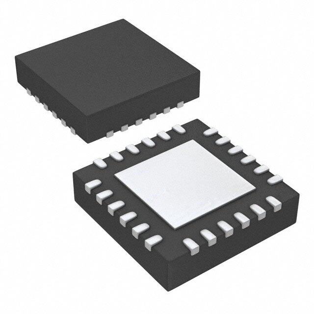
| 产品图片 |
|
| 产品型号 | TLC59208FIRGYR |
| rohs | 无铅 / 符合限制有害物质指令(RoHS)规范要求 |
| 产品系列 | - |
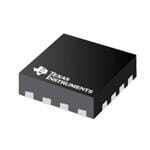
| 供应商器件封装 | 16-VQFN(4x4) |
| 其它名称 | 296-36989-6 |
| 内部驱动器 | 是 |
| 包装 | Digi-Reel® |
| 安装类型 | 表面贴装 |
| 封装/外壳 | 16-VFQFN 裸露焊盘 |
| 工作温度 | -40°C ~ 85°C |
| 恒压 | - |
| 恒流 | - |
| 拓扑 | 8 位移位寄存器,开路漏极,PWM |
| 标准包装 | 1 |
| 电压-电源 | 3 V ~ 5.5 V |
| 电压-输出 | 17V |
| 类型-初级 | 通用 |
| 类型-次级 | RGBA |
| 输出数 | 8 |
| 频率 | 25MHz |


- 商务部:美国ITC正式对集成电路等产品启动337调查
- 曝三星4nm工艺存在良率问题 高通将骁龙8 Gen1或转产台积电
- 太阳诱电将投资9.5亿元在常州建新厂生产MLCC 预计2023年完工
- 英特尔发布欧洲新工厂建设计划 深化IDM 2.0 战略
- 台积电先进制程称霸业界 有大客户加持明年业绩稳了
- 达到5530亿美元!SIA预计今年全球半导体销售额将创下新高
- 英特尔拟将自动驾驶子公司Mobileye上市 估值或超500亿美元
- 三星加码芯片和SET,合并消费电子和移动部门,撤换高东真等 CEO
- 三星电子宣布重大人事变动 还合并消费电子和移动部门
- 海关总署:前11个月进口集成电路产品价值2.52万亿元 增长14.8%


PDF Datasheet 数据手册内容提取
Product Sample & Technical Tools & Support & Folder Buy Documents Software Community TLC59208F SCLS715A–MARCH2009–REVISEDNOVEMBER2015 2 TLC59208F 8-Bit Fm+ I C Bus LED Driver 1 Features 1 • EightLEDDrivers(EachOutputProgrammableat • NoiseFilteronSCL/SDAInputs OFF,ON,ProgrammableLEDBrightness, • NoGlitchonPowerUp ProgrammableGroupDimming/BlinkingMixed • Active-LowReset(RESET) WithIndividualLEDBrightness) • SupportsHotInsertion • EightOpen-DrainOutputChannels • LowStandbyCurrent • 256-Step(8-Bit)LinearProgrammableBrightness • 3.3-Vor5-VSupplyVoltage PerLEDOutputVaryingFromFullyOff(Default) • 5.5-VTolerantInputs toMaximumBrightnessUsinga97-kHzPWM Signal • PackagesOffered:16-PinThinShrinkSmall- OutlinePackage[TSSOP(PW)],16-PinQuad • 256-StepGroupBrightnessControlAllows FlatpackNoLead[QFN(RGY)] GeneralDimming[Usinga190-HzPWMSignal FromFullyOfftoMaximumBrightness(Default)] • –40°Cto85°COperation • 256-StepGroupBlinkingWithFrequency 2 Applications ProgrammableFrom24Hzto10.73sandDuty CycleFrom0%to99.6% • Gaming • 64ProgrammableSlaveAddressesUsingThree • SmallSignage HardwareAddressPins • IndustrialEquipment • FourSoftwareProgrammableI2CBusAddresses (OneLEDGroupCallAddressandThreeLED 3 Description SubCallAddresses)AllowGroupsofDevicesto The TLC59208F is an I2C bus controlled 8-bit LED beSimultaneouslyAddressedAnyCombination driver optimized for red/green/blue/amber (RGBA) (ForExample,OneRegisterUsedfor ‘AllCall’so color mixing applications. Each LED output has its ThatAlltheTLC59208FsontheI2CBusCanbe own 8-bit resolution (256 steps) fixed frequency SimultaneouslyAddressedandtheSecond individual PWM controller that operates at 97 kHz RegisterUsedforThreeDifferentAddressesso with a duty cycle that is adjustable from 0% to 99.6% to allow the LED to be set to a specific brightness ThatOneThirdofAllDevicesontheBusCanbe value. SimultaneouslyAddressed) • SoftwareEnableandDisableforI2CBusAddress DeviceInformation(1) • SoftwareResetFeature(SWRSTCall)Allowsthe PARTNUMBER PACKAGE BODYSIZE(NOM) DevicetobeResetThroughtheI2CBus TSSOP(16) 5.00mm×4.40mm TLC59208F • Upto14PossibleHardwareAdjustableIndividual VQFN(16) 4.00mm×3.50mm I2CBusAddressesPerDevicesoThatEach (1) For all available packages, see the orderable addendum at DeviceCanbeProgrammed theendofthedatasheet. • Upto64PossibleHardwareAdjustableIndividual I2CBusAddressesPerDevicesoThatEach ApplicationSchematic DeviceCanbeProgrammedIndividually VLED • OutputStateChangeProgrammableonthe AcknowledgeortheSTOPCommandtoUpdate 3.3V or 5V OutputsByte-by-ByteorAllattheSameTime (DefaulttoChangeonSTOP) SCL VDD • MaximumOutputCurrent:50mA (cid:181)C SDA OUT7 • MaximumOutputVoltage:17V RESET • 25-MHzInternalOscillatorRequiresnoExternal A0-A2 OUT0 Components • 1-MHzFast-ModePlus(FM+)CompatibleI2CBus TLC59208F InterfaceWith30-mAHighDriveCapabilityon SDAOutputforDrivingHighCapacitiveBuses GND • InternalPower-OnReset 1 An IMPORTANT NOTICE at the end of this data sheet addresses availability, warranty, changes, use in safety-critical applications, intellectualpropertymattersandotherimportantdisclaimers.PRODUCTIONDATA.
TLC59208F SCLS715A–MARCH2009–REVISEDNOVEMBER2015 www.ti.com Table of Contents 1 Features.................................................................. 1 9.3 FeatureDescription...................................................9 2 Applications........................................................... 1 9.4 DeviceFunctionalModes........................................11 3 Description............................................................. 1 9.5 Programming...........................................................11 9.6 RegisterMaps.........................................................20 4 RevisionHistory..................................................... 2 10 ApplicationandImplementation........................ 25 5 Description(continued)......................................... 3 10.1 ApplicationInformation..........................................25 6 PinConfigurationandFunctions......................... 3 10.2 TypicalApplication ...............................................25 7 Specifications......................................................... 4 11 PowerSupplyRecommendations..................... 26 7.1 AbsoluteMaximumRatings......................................4 12 Layout................................................................... 27 7.2 ESDRatings..............................................................4 12.1 LayoutGuidelines.................................................27 7.3 RecommendedOperatingConditions......................5 12.2 LayoutExample....................................................27 7.4 ThermalInformation..................................................5 13 DeviceandDocumentationSupport................. 29 7.5 ElectricalCharacteristics...........................................5 7.6 I2CInterfaceTimingRequirements...........................6 13.1 Trademarks...........................................................29 7.7 TypicalCharacteristics..............................................8 13.2 CommunityResources..........................................29 13.3 ElectrostaticDischargeCaution............................29 8 ParameterMeasurementInformation..................8 13.4 Glossary................................................................29 9 DetailedDescription.............................................. 9 14 Mechanical,Packaging,andOrderable 9.1 Overview...................................................................9 Information........................................................... 29 9.2 FunctionalBlockDiagram.........................................9 4 Revision History NOTE:Pagenumbersforpreviousrevisionsmaydifferfrompagenumbersinthecurrentversion. ChangesfromOriginal(March2009)toRevisionA Page • AddedPinConfigurationandFunctionssection,ESDRatingstable,FeatureDescriptionsection,DeviceFunctional Modes,ApplicationandImplementationsection,PowerSupplyRecommendationssection,Layoutsection,Device andDocumentationSupportsection,andMechanical,Packaging,andOrderableInformationsection .............................. 1 2 SubmitDocumentationFeedback Copyright©2009–2015,TexasInstrumentsIncorporated ProductFolderLinks:TLC59208F
TLC59208F www.ti.com SCLS715A–MARCH2009–REVISEDNOVEMBER2015 5 Description (continued) An additional 8-bit resolution (256 steps) group PWM controller has both a fixed frequency of 190 Hz and an adjustable frequency between 24 Hz to once every 10.73 seconds with a duty cycle that is adjustable from 0% to 99.6%thatisusedtoeitherdimorblinkallLEDswiththesamevalue. Each LED output can be off, on (no PWM control), set at its individual PWM controller value or at both individual and group PWM controller values. The TLC59208F operates with a supply voltage range of 3 V to 5.5 V and the outputsare17Vtolerant.LEDscanbedirectlyconnectedtotheTLC59208Fdeviceoutputs. Software programmable LED Group and three Sub Call I2C bus addresses allow all or defined groups of TLC59208F devices to respond to a common I2C bus address, allowing for example, all the same color LEDs to beturnedonoroffatthesametimeormarqueechasingeffect,thusminimizingI2Cbuscommands. Threehardwareaddresspinsallowupto64devicesonthesamebus. The software reset (SWRST) Call allows the master to perform a reset of the TLC59208F through the I2C bus, identical to the power-on reset (POR) that initializes the registers to their default state causing the outputs to be sethigh(LEDoff).Thisallowsaneasyandquickwaytoreconfigurealldeviceregisterstothesamecondition. 6 Pin Configuration and Functions PWPackage 16-PinTSSOP RGYPackage TopView 16-PinVQFNWithExposedThermalPad TopView A0 1 16 VCC A0 VCC A1 2 15 SDA A2 3 14 SCL 1 16 OUT0 4 13 RESET A1 2 15 SDA OUT1 5 12 OUT7 A2 3 14 SCL OUT2 6 11 OUT6 OUT0 4 13 RESET OUT3 7 10 OUT5 GND 8 9 OUT4 OUT1 5 12 OUT7 OUT2 6 11 OUT6 OUT3 7 10 OUT5 8 9 GND OUT4 PinFunctions PIN I/O(1) DESCRIPTION NAME NO. A0 1 I Addressinput0 A1 2 I Addressinput1 A2 3 I Addressinput2 GND 8 — Ground OUT0 4 OUT1 5 OUT2 6 OUT3 7 O Open-drainoutput0to7,LEDONatlow OUT4 9 OUT5 10 OUT6 11 OUT7 12 RESET 13 I Active-lowresetinput SCL 14 I Serialclockinput (1) I=input,O=output Copyright©2009–2015,TexasInstrumentsIncorporated SubmitDocumentationFeedback 3 ProductFolderLinks:TLC59208F
TLC59208F SCLS715A–MARCH2009–REVISEDNOVEMBER2015 www.ti.com PinFunctions(continued) PIN I/O(1) DESCRIPTION NAME NO. SDA 15 I/O Serialdatainput/output V 16 — Powersupply CC 7 Specifications 7.1 Absolute Maximum Ratings overoperatingfree-airtemperaturerange(unlessotherwisenoted)(1) MIN MAX UNIT V Supplyvoltage 0 7 V CC V Inputvoltage –0.4 7 V I V Outputvoltage –0.5 20 V O I Continuousoutputcurrent 50 mA O PWpackage(2) 108 θ Packagethermalimpedance °C/W JA RGYpackage(3) 39 PWpackage 0.90 P PowerDissipation,T =25°C,JESD51-7 W D A RGYpackage 2.08 T Junctiontemperature –40 150 °C J T Storagetemperature –55 150 °C stg (1) StressesbeyondthoselistedunderAbsoluteMaximumRatingsmaycausepermanentdamagetothedevice.Thesearestressratings only,whichdonotimplyfunctionaloperationofthedeviceattheseoranyotherconditionsbeyondthoseindicatedunderRecommended OperatingConditions.Exposuretoabsolute-maximum-ratedconditionsforextendedperiodsmayaffectdevicereliability. (2) ThepackagethermalimpedanceiscalculatedinaccordancewithJESD51-7. (3) ThepackagethermalimpedanceiscalculatedinaccordancewithJESD51-5. 7.2 ESD Ratings VALUE UNIT Humanbodymodel(HBM),perANSI/ESDA/JEDECJS-001(1) ±2000 V(ESD) Electrostaticdischarge Charged-devicemodel(CDM),perJEDECspecificationJESD22- ±500 V C101(2) (1) JEDECdocumentJEP155statesthat500-VHBMallowssafemanufacturingwithastandardESDcontrolprocess. (2) JEDECdocumentJEP157statesthat250-VCDMallowssafemanufacturingwithastandardESDcontrolprocess. 4 SubmitDocumentationFeedback Copyright©2009–2015,TexasInstrumentsIncorporated ProductFolderLinks:TLC59208F
TLC59208F www.ti.com SCLS715A–MARCH2009–REVISEDNOVEMBER2015 7.3 Recommended Operating Conditions overoperatingfree-airtemperaturerange(unlessotherwisenoted)(1) MIN MAX UNIT V Supplyvoltage 3 5.5 V CC V High-levelinputvoltage SCL,SDA,RESET,A0,A1,A2 0.7×V 5.5 V IH CC V Low-levelinputvoltage SCL,SDA,RESET,A0,A1,A2 0 0.3×V V IL CC V Outputvoltage OUT0toOUT7 17 V O V =3V 20 CC I Low-leveloutputcurrent SDA mA OL V =4.5V 30 CC I Outputcurrent OUT0toOUT7 50 mA O T Operatingfree-airtemperature –40 85 °C A (1) AllunusedinputsofthedevicemustbeheldatV orGNDtoensureproperdeviceoperation. CC 7.4 Thermal Information TLC59208F THERMALMETRIC(1) PW(TSSOP) RGY(VQFN) UNIT 16PINS 16PINS R Junction-to-ambientthermalresistance 108 39 °C/W θJA (1) Formoreinformationabouttraditionalandnewthermalmetrics,seetheSemiconductorandICPackageThermalMetricsapplication report,SPRA953. 7.5 Electrical Characteristics V =3Vto5.5V,T =–40°Cto85°C(unlessotherwisenoted) CC A PARAMETER TESTCONDITIONS MIN TYP(1) MAX UNIT SCL,SDA,A0, Input/outputleakage I A1,A2, V =V orGND ±0.3 μA I current I CC RESET Outputleakage OUT0toOUT7 V =17V,T =25°C 0.5 μA current O J V Power-onresetvoltage 2.5 V POR Low-leveloutput VCC=3V,VOL=0.4V 20 I SDA mA OL current V =4.5V,V =0.4V 30 CC OL Low-leveloutput VCC=3V,IOL=50mA 108 185 V OUT0toOUT7 mV OL voltage V =4.5V,I =50mA 90 165 CC OL V =3V,I =50mA 2 3.75 CC OL r ON-stateresistance OUT0toOUT7 Ω ON V =4.5V,I =50mA 1.8 3.3 CC OL T Thermalshutdowntemperature(2) 150 175 200 °C SD T Restarthysteresis 15 °C HYS SCL,A0,A1, C Inputcapacitance V =V orGND 6 pF i A2,RESET I CC Input/output C SDA V =V orGND 8 pF io capacitance I CC V =3.3V,OUT0toOUT7=OFF 5 CC I Supplycurrent mA CC V =5.5V,OUT0toOUT7=OFF 8 CC (1) AlltypicalvaluesareatT =25°C. J (2) Specifiedbydesign,notproductiontested. Copyright©2009–2015,TexasInstrumentsIncorporated SubmitDocumentationFeedback 5 ProductFolderLinks:TLC59208F
TLC59208F SCLS715A–MARCH2009–REVISEDNOVEMBER2015 www.ti.com 7.6 I2C Interface Timing Requirements T =–40°Cto85°C A STANDARD-MODE FAST-MODE FAST-MODEPLUS I2CBUS I2CBUS I2CBUS UNIT MIN MAX MIN MAX MIN MAX I2CINTERFACE f SCLclockfrequency 0 100 0 400 0 1000 kHz SCL I2Cbusfreetimebetweenstopand t 4.7 1.3 0.5 μs BUF start t Holdtime(repeated)Startcondition 4 0.6 0.26 μs HD;STA Set-uptimeforarepeatedStart t 4.7 0.6 0.26 μs SU;STA condition t Set-uptimeforStopcondition 4 0.6 0.26 μs SU;STO t Dataholdtime 0 0 0 ns HD;DAT t Datavalidacknowledgetime(1) 0.3 3.45 0.1 0.9 0.05 0.45 μs VD;ACK t Datavalidtime(2) 0.3 3.45 0.1 0.9 0.05 0.45 μs VD;DAT t Dataset-uptime 250 100 50 ns SU;DAT t LowperiodoftheSCLclock 4.7 1.3 0.5 μs LOW t HighperiodoftheSCLclock 4 0.6 0.26 μs HIGH tf Fsiaglnlatilms(e3)o(f4)bothSDAandSCL 300 20+0.1Cb (5) 300 120 ns t RisetimeofbothSDAandSCL 1000 20+0.1C (5) 300 120 ns r signals b Pulsewidthofspikesthatmustbe tSP suppressedbytheinputfilter(6) 50 50 50 ns RESET t Resetpulsewidth 10 10 10 ns W t Resetrecoverytime 0 0 0 ns REC t Timetoreset(7) (8) 400 400 400 ns RESET (1) t =timeforAcknowledgementsignalfromSCLlowtoSDA(out)low. VD;ACK (2) t =minimumtimeforSDAdataouttobevalidfollowingSCLlow. VD;DAT (3) Amasterdevicemustinternallyprovideaholdtimeofatleast300nsfortheSDAsignal(refertotheVILoftheSCLsignal)inorderto bridgetheundefinedregionofSCLsfallingedge. (4) ThemaximumtffortheSDAandSCLbuslinesisspecifiedat300ns.Themaximumfalltime(t)fortheSDAoutputstageisspecified f at250ns.ThisallowsseriesprotectionresistorstobeconnectedbetweentheSDAandtheSCLpinsandtheSDA/SCLbuslines withoutexceedingthemaximumspecifiedt. f (5) C =totalcapacitanceofonebuslineinpF. b (6) InputfiltersontheSDAandSCLinputssuppressnoisespikeslessthan50ns (7) ResettingthedevicewhileactivelycommunicatingonthebusmaycauseglitchesorerrantStopconditions. (8) Uponreset,thefulldelaywillbethesumoft andtheRCtimeconstantoftheSDAbus. RESET 6 SubmitDocumentationFeedback Copyright©2009–2015,TexasInstrumentsIncorporated ProductFolderLinks:TLC59208F
TLC59208F www.ti.com SCLS715A–MARCH2009–REVISEDNOVEMBER2015 START SCL ACK OR READ CYCLE SDA 30% t RESET RESET 50% t REC t W OUTn 50% t RESET Figure1. DefinitionofRESETTiming SDA t BUF t t HD;STA SP tr tf t LOW SCL t t t HD;STA SU;DAT SU;STO P S tHD;DAT tHIGH tSU;DAT Sr P Figure2. DefinitionofTiming Start Bit 7 Stop Bit 6 Bit 7 Bit 8 Acknowledge Protocol Condition MSB Condition (A6) (D1) (D0) (A) (S) (A7) (P) tSU;STA tLOW tHIGH 1/fSCL SCL t r t f t BUF SDA t t t t t t HD;STA SU;DAT HD;DAT VD;DAT VD;ACK SU;STO NOTE: RiseandfalltimesrefertoV andV . IL IH Figure3. I2CBusTiming Copyright©2009–2015,TexasInstrumentsIncorporated SubmitDocumentationFeedback 7 ProductFolderLinks:TLC59208F
TLC59208F SCLS715A–MARCH2009–REVISEDNOVEMBER2015 www.ti.com 7.7 Typical Characteristics 2 108 1.975 106 104 1.95 102 1.925 :) mV) 100 (ON 1.9 (OL 98 r V 1.875 96 1.85 94 1.825 92 1.8 90 3 3.2 3.4 3.6 3.8 4 4.2 4.4 4.6 3 3.2 3.4 3.6 3.8 4 4.2 4.4 4.6 Vcc (V) Vcc (V) D001 D001 I =50mA I =50mA OL OL Figure4.r vsVcc Figure5.V vsVcc ON OL 8 Parameter Measurement Information V DD V Open DD GND R L V V Pulse I O DUT Generator RT CL NOTE: R =LoadresistanceforSDAandSCL;shouldbe>1kΩat3-mAorlowercurrent. L C =Loadcapacitance;includesjigandprobecapacitance. L R =Terminationresistance;shouldbeequaltotheoutputimpedance(Z )ofthepulsegenerator. T O Figure6. TestCircuitforSwitchingCharacteristics 8 SubmitDocumentationFeedback Copyright©2009–2015,TexasInstrumentsIncorporated ProductFolderLinks:TLC59208F
TLC59208F www.ti.com SCLS715A–MARCH2009–REVISEDNOVEMBER2015 9 Detailed Description 9.1 Overview The TLC59208F is an I2C bus controlled 8-bit LED driver optimized for red, green, blue, or amber (RGBA) colormixing applications. Each LED output has its own 8-bit resolution (256 steps) fixed frequency individual PWMcontrollerthatoperatesat97kHzwithadutycycleadjustablefrom0%to99.6%toallowtheLEDtobeset to a specific brightness value. An additional 8-bit resolution (256 steps) group PWM controller has both a fixed frequency of 190 Hz and an adjustable frequency between 24 Hz to once every 10.73 seconds with a duty cycle adjustablefrom0%to99.6%thatcaneitherdimorblinkallLEDswiththesamevalue. Each LED output can be off, on (no PWM control), set at its individual PWM controller value or at both individual and group PWM controller values. The TLC59208F operates with a supply voltage range of 3 V to 5.5 V and the outputsare17Vtolerant.LEDscanbedirectlyconnectedtotheTLC59208Fdeviceoutputs. Software programmable LED group and three sub call I2C bus addresses allow all or defined groups of TLC59208F devices to respond to a common I2C bus address, allowing for example, all the same color LEDs to beturnedonoroffatthesametimeormarqueechasingeffect,thusminimizingI2Cbuscommands. The software reset (SWRST) call allows the master to perform a reset of the TLC59208F through the I2C bus, identical to the power-on reset (POR) that initializes the registers to their default state causing the outputs to be sethigh(LEDoff).Thisallowsaneasyandquickwaytoreconfigurealldeviceregisterstothesamecondition. 9.2 Functional Block Diagram A0 A1 A2 OUT0 OUT1 OUT6 OUT7 SCL INPUT FILTER SDA 2 I C BUS CONTROL POWER-ON OUTPUT DRIVER AND RESET RESET CONTROL ERROR DETECTION LED STATE PWM SELECT REGISTERX REGISTER BRIGHTNESS CONTROL GRPFREQ 97kHz 24.3kHz REGISTER GRPPWM REGISTER 25 MHz OSCILLATOR 190 Hz ‘0’– Permanently OFF VCC ‘1’– Permanently ON GND TLC59208F NOTE: OnlyonePWMshownforclarity. 9.3 Feature Description 9.3.1 Power-OnReset WhenpowerisappliedtoV ,aninternalpower-onresetholdstheTLC59208FinaresetconditionuntilV has CC CC reached V . At this point, the reset condition is released and the TLC59208F registers and I2C bus state POR machine are initialized to their default states causing all the channels to be deselected. Thereafter, V must be CC loweredbelow0.2Vtoresetthedevice. Copyright©2009–2015,TexasInstrumentsIncorporated SubmitDocumentationFeedback 9 ProductFolderLinks:TLC59208F
TLC59208F SCLS715A–MARCH2009–REVISEDNOVEMBER2015 www.ti.com Feature Description (continued) 9.3.2 ExternalReset A reset can be accomplished by holding the RESET pin low for a minimum of tW. The TLC59208F registers and I2CstatemachinewillbeheldintheirdefaultstateuntiltheRESETinputisonceagainhigh. Thisinputrequiresapull-upresistortoV ifnoactiveconnectionisused. CC 9.3.3 SoftwareReset The Software Reset Call (SWRST Call) allows all the devices in the I2C bus to be reset to the power-up state value through a specific I2C bus command. To be performed correctly, the I2C bus must be functional and there mustbenodevicehangingthebus. TheSWRSTCallfunctionisdefinedasthefollowing: 1. AStartcommandissentbytheI2Cbusmaster. 2. The reserved SWRST I2C bus address 1001 111 with the R/W bit set to 0 (write) is sent by the I2C bus master. 3. The TLC59208F device(s) acknowledge(s) after seeing the SWRST Call address 1001 0110 (9Eh) only. If theR/Wbitissetto1(read),noacknowledgeisreturnedtotheI2Cbusmaster. 4. Once the SWRST Call address has been sent and acknowledged, the master sends two bytes with two specificvalues(SWRSTdatabyte1andbyte2): (a) Byte1=A5h:theTLC59208Facknowledgesthisvalueonly.Ifbyte1isnotequaltoA5h,theTLC59208F doesnotacknowledgeit. (b) Byte 2 = 5Ah: the TLC59208F acknowledges this value only. If byte 2 is not equal to 5Ah, the TLC59208Fdoesnotacknowledgeit. Ifmorethantwobytesofdataaresent,theTLC59208Fdoesnotacknowledgeanymore. 5. Once the correct two bytes (SWRST data byte 1 and byte 2 only) have been sent and correctly acknowledged, the master sends a Stop command to end the SWRST Call. The TLC59208F then resets to the default value (power-up value) and is ready to be addressed again within the specified bus free time (t ). BUF The I2C bus master may interpret a non-acknowledge from the TLC59208F (at any time) as a SWRST Call Abort. The TLC59208F does not initiate a reset of its registers. This happens only when the format of the Start Callsequenceisnotcorrect. 9.3.4 IndividualBrightnessControlWithGroupDimming/Blinking A 97-kHz fixed frequency signal with programmable duty cycle (8 bits, 256 steps) is used to control individually thebrightnessforeachLED. On top of this signal, one of the following signals can be superimposed (this signal can be applied to the 4 LED outputs): • A lower 190-Hz fixed frequency signal with programmable duty cycle (8 bits, 256 steps) is used to provide a globalbrightnesscontrol. • A programmable frequency signal from 24 Hz to 1/10.73 s (8 bits, 256 steps) is used to provide a global blinkingcontrol. 10 SubmitDocumentationFeedback Copyright©2009–2015,TexasInstrumentsIncorporated ProductFolderLinks:TLC59208F
TLC59208F www.ti.com SCLS715A–MARCH2009–REVISEDNOVEMBER2015 Feature Description (continued) 508 510 512 508 510 512 1 2 3 4 5 6 7 8 9 10 11 12 507 508 511 507 508 511 1 2 3 4 5 6 7 8 9 10 11 NX40 ns with N = (0 to 255) (PWMx Register) MX256X2X40 ns 258X40 ns = 10.24µs with M = (0 to 255) (97.6 kHz) (GRPPWM Register) Group Dimming Signal 256X2X256X40 ns = 5.24 ms (190.7 Hz) 1 2 3 4 5 6 7 8 1 2 3 4 5 6 7 8 Resulting Brightness + Group Dimming Signal A. MinimumpulsewidthforLEDnbrightnesscontrolis40ns. B. Minimumpulsewidthforgroupdimmingis20.48μs. C. WhenM=1(GRPPWMregistervalue),theresultingLEDnbrightnesscontrolandgroupdimmingsignalwillhavetwo pulsesoftheLEDbrightnesscontrolsignal(pulsewidth=N×40ns,withNdefinedinthePWMxregister). D. TheresultingbrightnessplusgroupdimmingsignalshownabovedemonstratearesultingcontrolsignalwithM=4(8 pulses). Figure7. Brightness+GroupDimmingSignals 9.4 Device Functional Modes Active Activemodeoccurswhenoneormoreoftheoutputchannelsisenabled. Standby Standbymodeoccurswhenalloutputchannelsaredisabled.Standbymodemaybeenteredeither throughI2CcommandorbypullingtheRESETpinlow. 9.5 Programming 9.5.1 CharacteristicsoftheI2CBus The I2C bus is for two-way two-line communication between different devices or modules. The two lines are a serial data line (SDA) and a serial clock line (SCL). Both lines must be connected to a positive supply via a pullupresistorwhenconnectedtotheoutputstagesofadevice.Datatransfermaybeinitiatedonlywhenthebus isnotbusy. 9.5.1.1 BitTransfer One data bit is transferred during each clock pulse. The data on the SDA line must remain stable during the high period of the clock pulse as changes in the data line at this time will be interpreted as control signals (see Figure8). Copyright©2009–2015,TexasInstrumentsIncorporated SubmitDocumentationFeedback 11 ProductFolderLinks:TLC59208F
TLC59208F SCLS715A–MARCH2009–REVISEDNOVEMBER2015 www.ti.com Programming (continued) SDA SCL Data Line Change Stable; of Data DataValid Allowed Figure8. BitTransfer 9.5.1.2 StartandStopConditions Both data and clock lines remain high when the bus is not busy. A high-to-low transition of the data line while the clockishighisdefinedastheStartcondition(S).Alow-to-hightransitionofthedatalinewhiletheclockishighis definedastheStopcondition(P)(seeFigure9). SDA SDA SCL SCL S P Start Condition Stop Condition Figure9. StartandStopConditions 12 SubmitDocumentationFeedback Copyright©2009–2015,TexasInstrumentsIncorporated ProductFolderLinks:TLC59208F
TLC59208F www.ti.com SCLS715A–MARCH2009–REVISEDNOVEMBER2015 Programming (continued) 9.5.2 SystemConfiguration A device generating a message is a transmitter; a device receiving is the receiver. The device that controls the messageisthemasterandthedeviceswhicharecontrolledbythemasteraretheslaves(seeFigure10). SDA SCL Master Slave Master Master I 2C Bus Transmitter/ Slave Receiver Transmitter/ Transmitter/ Transmitter Multiplexer Receiver Receiver Receiver Slave Figure10. SystemConfiguration 9.5.3 Acknowledge The number of data bytes transferred between the Start and the Stop conditions from transmitter to receiver is notlimited.Eachbyteofeightbitsisfollowedbyoneacknowledgebit.Theacknowledgebitisahighlevelputon thebusbythetransmitter,whereasthemastergeneratesanextraacknowledgerelatedclockpulse. A slave receiver which is addressed must generate an acknowledge after the reception of each byte. Also a master must generate an acknowledge after the reception of each byte that has been clocked out of the slave transmitter. The device that acknowledges has to pull down the SDA line during the acknowledge clock pulse, so that the SDA line is stable low during the high period of the acknowledge related clock pulse; set-up time and holdtimemustbetakenintoaccount. A master receiver must signal an end of data to the transmitter by not generating an acknowledge on the last byte that has been clocked out of the slave. In this event, the transmitter must leave the data line high to enable themastertogenerateaStopcondition. Data Output byTransmitter NACK Data Output by Receiver ACK SCL From Master 1 2 8 9 S Start Clock Pulse for Condition Acknowledgment Figure11. AcknowledgeonI2CBus Copyright©2009–2015,TexasInstrumentsIncorporated SubmitDocumentationFeedback 13 ProductFolderLinks:TLC59208F
TLC59208F SCLS715A–MARCH2009–REVISEDNOVEMBER2015 www.ti.com Programming (continued) Slave Address Control Register S A6 A5 A4 A3 A2 A1 A0 0 A X X X D4 D3 D2 D1 D0 A A P Auto-Increment Options START Condition R/W Auto-Increment Flag SCToOndPition Acknowledge Acknowledge Acknowledge From Slave From Slave From Slave Figure12. WritetoaSpecificRegister Slave Address Control Register MODE1 Register MODE2 Register S A6 A5 A4 A3 A2 A1 A0 0 A 1 0 0 0 0 0 0 0 A A A (cont.) START Condition R/W AAull tRo-eIngcisrteemrsent on MSeOleDcEti1o nRegister Acknowledge (except reg IC–IF) Acknowledge Acknowledge Acknowledge From Slave From Slave From Slave From Slave Auto-Increment On SUBADR3 Register ALLCALLADR Register (cont.) A A P Acknowledge Acknowledge From Slave From Slave STOP Condition Figure13. WritetoAllRegistersUsingAuto-Increment Slave Address Control Register PWM0 Register PWM1 Register S A6 A5 A4 A3 A2 A1 A0 0 A 1 0 1 0 0 0 1 0 A A A (cont.) START Condition R/W ABuritgoh-tInnecrsesm Reengt isotners PWSMel eRcetigoinster Acknowledge Only Acknowledge Acknowledge Acknowledge From Slave From Slave From Slave From Slave Auto-Increment On PWM14 Register PWM15 Register PWM0 Register PWMx Register (cont.) A A A A P Acknowledge Acknowledge Acknowledge Acknowledge From Slave From Slave From Slave From Slave STOP Condition Figure14. MultipleWritestoIndividualBrightnessRegistersOnlyUsingtheAuto-IncrementFeature 14 SubmitDocumentationFeedback Copyright©2009–2015,TexasInstrumentsIncorporated ProductFolderLinks:TLC59208F
TLC59208F www.ti.com SCLS715A–MARCH2009–REVISEDNOVEMBER2015 Programming (continued) Slave Address Control Register Slave Address Data from MODE1 Register S A6 A5 A4 A3 A2 A1 A0 0 A 1 0 1 0 0 0 1 0 A Sr A6 A5 A4 A3 A2 A1 A0 1 A A A (cont.) START Condition R/W Aonu tAo-llI nRceregmisteenrst MOSDeEl1eRcteiognister R/W AFcrkonmo wMleadstgeer Acknowledge Acknowledge Acknowledge From Slave From Slave From Slave Auto-Increment On Data from MODE2 Register Data from PWM0 Register Data from ALLCALLADR Register Data from MODE1 Register (cont.) A A A A (cont.) Acknowledge Acknowledge Acknowledge Acknowledge From Master From Master From Master From Master Data from Last Read Byte (cont.) A P Not Acknowledge From Master STOP Condition Figure15. ReadAllRegistersWiththeAuto-IncrementFeature Slave Address Control Register New LED All-Call I2 C Address(B) Sequence A S A6 A5 A4 A3 A2 A1 A0 0 A X X X 1 1 0 1 1 A 1 1 0 1 1 0 1 X A P START Condition R/W ReAgLisLtCeAr SLLeAleDctRion AcFkrnoomw Sleldagvee Acknowledge Acknowledge STOP From Slave From Slave Condition Auto-Increment Flag The 16 LEDs are ON at Acknowledge LED All-Call I 2C Address Control Register LEDOUT0 Register (LED0–LED3 Fully ON)(C) Sequence B S 1 0 0 1 1 0 1 0 A X X X 1 0 1 0 0 A 0 1 0 1 0 1 0 1 A P START Condition R/W LEDOUT0 Register Selection Acknowledge From Slave Acknowledge Acknowledge STOP From Slave From the 4 Devices Condition Auto-Increment Flag A. Inthisexample,severalTLC59208Fsareusedwiththesamesequencesenttoeach. B. ALLCALLbitinMODE1registerisequalto1forthisexample. C. OCHbitinMODE2registerisequalto1forthisexample. Figure16. LEDAll-CallI2CBusAddressProgrammingandLEDAll-CallSequenceExample 9.5.4 DeviceAddress FollowingaStartcondition,thebusmastermustoutputtheaddressoftheslaveitisaccessing. Copyright©2009–2015,TexasInstrumentsIncorporated SubmitDocumentationFeedback 15 ProductFolderLinks:TLC59208F
TLC59208F SCLS715A–MARCH2009–REVISEDNOVEMBER2015 www.ti.com Programming (continued) 9.5.5 RegularI2CBusSlaveAddress The I2C bus slave address of the TLC59208F is shown in Figure 17. Slave address pins A0, A1, and A2 choose 1 of 64 slave addresses. To conserve power, no internal pullup resistors are incorporated on A0, A1, or A2. Addressvalues,dependingonA0,A1,andA2,canbefoundinTable1. NOTE When using the TLC59208F, reserved I2C bus addresses must be used with caution since theycaninterferewiththefollowing: • ReservedforfutureuseI2Cbusaddresses(0000011,1111101,1111110,1111111) • Slavedevicesthatusethe10-bitaddressingscheme(11110xx) • High-speedmodemastercode(00001xx) Slave Address A6 A5 A4 A3 A2 A1 A0 R/W Programmable Figure17. SlaveAddress The last bit of the address byte defines the operation to be performed. When set to logic 1, a read operation is selected.Whensettologic0,awriteoperationisselected. 9.5.5.1 RegularI2CBusSlaveAddress Table1.TLC59208FAddressMap ADDRESSINPUT SLAVEADDRESS A2 A1 A0 A6 A5 A4 A3 A2 A1 A0 ADDRESS GND SCL GND 0 0 1 0 0 0 0 20h GND SCL V 0 0 1 0 0 0 1 22h CC GND SDA GND 0 0 1 0 0 1 0 24h GND SDA V 0 0 1 0 0 1 1 26h CC V SCL GND 0 0 1 0 1 0 0 28h CC V SCL V 0 0 1 0 1 0 1 2Ah CC CC V SDA GND 0 0 1 0 1 1 0 2Ch CC V SDA V 0 0 1 0 1 1 1 2Eh CC CC GND SCL SCL 0 0 1 1 0 0 0 30h GND SCL SDA 0 0 1 1 0 0 1 32h GND SDA SCL 0 0 1 1 0 1 0 34h GND SDA SDA 0 0 1 1 0 1 1 36h V SCL SCL 0 0 1 1 1 0 0 38h CC V SCL SDA 0 0 1 1 1 0 1 3Ah CC V SDA SCL 0 0 1 1 1 1 0 3Ch CC V SDA SDA 0 0 1 1 1 1 1 3Eh CC GND GND GND 0 1 0 0 0 0 0 40h GND GND V 0 1 0 0 0 0 1 42h CC GND V GND 0 1 0 0 0 1 0 44h CC GND V V 0 1 0 0 0 1 1 46h CC CC V GND GND 0 1 0 0 1 0 0 48h CC 16 SubmitDocumentationFeedback Copyright©2009–2015,TexasInstrumentsIncorporated ProductFolderLinks:TLC59208F
TLC59208F www.ti.com SCLS715A–MARCH2009–REVISEDNOVEMBER2015 Programming (continued) Table1.TLC59208FAddressMap(continued) ADDRESSINPUT SLAVEADDRESS A2 A1 A0 A6 A5 A4 A3 A2 A1 A0 ADDRESS V GND V 0 1 0 0 1 0 1 4Ah CC CC V V GND 0 1 0 0 1 1 0 4Ch CC CC V V V 0 1 0 0 1 1 1 4Eh CC CC CC GND GND SCL 0 1 0 1 0 0 0 50h GND GND SDA 0 1 0 1 0 0 1 52h GND V SCL 0 1 0 1 0 1 0 54h CC GND V SDA 0 1 0 1 0 1 1 56h CC V GND SCL 0 1 0 1 1 0 0 58h CC V GND SDA 0 1 0 1 1 0 1 5Ah CC V V SCL 0 1 0 1 1 1 0 5Ch CC CC V V SDA 0 1 0 1 1 1 1 5Eh CC CC SCL SCL GND 1 0 1 0 0 0 0 A0h SCL SCL V 1 0 1 0 0 0 1 A2h CC SCL SDA GND 1 0 1 0 0 1 0 A4h SCL SDA V 1 0 1 0 0 1 1 A6h CC SDA SCL GND 1 0 1 0 1 0 0 A8h SDA SCL V 1 0 1 0 1 0 1 AAh CC SDA SDA GND 1 0 1 0 1 1 0 ACh SDA SDA V 1 0 1 0 1 1 1 AEh CC SCL SCL SCL 1 0 1 1 0 0 0 B0h SCL SCL SDA 1 0 1 1 0 0 1 B2h SCL SDA SCL 1 0 1 1 0 1 0 B4h SCL SDA SDA 1 0 1 1 0 1 1 B6h SDA SCL SCL 1 0 1 1 1 0 0 B8h SDA SCL SDA 1 0 1 1 1 0 1 BAh SDA SDA SCL 1 0 1 1 1 1 0 BCh SDA SDA SDA 1 0 1 1 1 1 1 BEh SCL GND GND 1 1 0 0 0 0 0 C0h SCL GND V 1 1 0 0 0 0 1 C2h CC SCL V GND 1 1 0 0 0 1 0 C4h CC SCL V V 1 1 0 0 0 1 1 C6h CC CC SDA GND GND 1 1 0 0 1 0 0 C8h SDA GND V 1 1 0 0 1 0 1 CAh CC SDA V GND 1 1 0 0 1 1 0 CCh CC SDA V V 1 1 0 0 1 1 1 CEh CC CC SCL GND SCL 1 1 1 0 0 0 0 E0h SCL GND SDA 1 1 1 0 0 0 1 E2h SCL V SCL 1 1 1 0 0 1 0 E4h CC SCL V SDA 1 1 1 0 0 1 1 E6h CC SDA GND SCL 1 1 1 0 1 0 0 E8h SDA GND SDA 1 1 1 0 1 0 1 EAh SDA V SCL 1 1 1 0 1 1 0 ECh CC SDA V SDA 1 1 1 0 1 1 1 EEh CC Copyright©2009–2015,TexasInstrumentsIncorporated SubmitDocumentationFeedback 17 ProductFolderLinks:TLC59208F
TLC59208F SCLS715A–MARCH2009–REVISEDNOVEMBER2015 www.ti.com 9.5.6 LEDAllCallI2CBusAddress • Defaultpower-upvalue(ALLCALLADRaddressregister):90hor1001000 • ProgrammablethroughI2Cbus(volatileprogramming) • Atpower-up,LEDAllCallI2Cbusaddressisenabled.TLC59208FsendsanACKwhen90h(R/W=0)or91h (R/W=1)issentbythemaster. NOTE The default LED All Call I2C bus address (90h or 1001 000) must not be used as a regular I2C bus slave address since this address is enabled at power-up. All the TLC59208Fs on theI2CbuswillacknowledgetheaddressifsentbytheI2Cbusmaster. 9.5.7 LEDSubCallI2CBusAddress • ThreedifferentI2Cbusaddressescanbeused • Defaultpower-upvalues: – SUBADR1register:92hor1001001 – SUBADR2register:94hor1001010 – SUBADR3register:98hor1001100 • ProgrammablethroughI2Cbus(volatileprogramming) • At power-up, Sub Call I2C bus address is disabled. TLC59208F does not send an ACK when 92h (R/W = 0) or93h(R/W=1)or94h(R/W=0)or95h(R/W=1)or98h(R/W=0)or99h(R/W=1)issentbythemaster. NOTE The default LED Sub Call I2C bus address may be used as a regular I2C bus slave addressaslongastheSUBADRxbitsaredisabled. 9.5.8 SoftwareResetI2CBusAddress The address shown in Figure 18 is used when a reset of the TLC59208F needs to be performed by the master. The software reset address (SWRST Call) must be used with R/W = 0. If R/W = 1, the TLC59208F does not acknowledgetheSWRST.SeeSoftwareResetformoredetail. R/W 1 0 0 1 0 1 1 0 Figure18. SoftwareResetAddress NOTE The Software Reset I2C bus address is a reserved address and cannot be use as a regularI2CbusslaveaddressorasanLEDAllCallorLEDSubCalladdress. 9.5.9 ControlRegister Following the successful acknowledgement of the slave address, LED All Call address or LED Sub Call address, the bus master will send a byte to the TLC59208F, which will be stored in the Control register. The lowest 5 bits are used as a pointer to determine which register will be accessed (D[4:0]). The highest 3 bits are used as Auto- IncrementflagandAuto-Incrementoptions(AI[2:0]). 18 SubmitDocumentationFeedback Copyright©2009–2015,TexasInstrumentsIncorporated ProductFolderLinks:TLC59208F
TLC59208F www.ti.com SCLS715A–MARCH2009–REVISEDNOVEMBER2015 Auto-Increment Register Address Flag A I2 A I1 AI0 D4 D3 D2 D1 D0 Auto-Increment Options Figure19. ControlRegister When the Auto-Increment flag is set (AI2 = logic 1), the five low order bits of the Control register are automatically incremented after a read or write. This allows the user to program the registers sequentially. Four differenttypesofAuto-Incrementarepossible,dependingonAI1andAI0values. Table2.Auto-IncrementOptions(1) AI2 AI1 AI0 DESCRIPTION 0 0 0 Noauto-increment Auto-incrementforallregisters.D[4:0]rolloverto'00000'afterthelastregister('10001')is 1 0 0 accessed. Auto-incrementforindividualbrightnessregistersonly.D[4:0]rolloverto'00010'afterthelast 1 0 1 register('01001')isaccessed. Auto-incrementforglobalcontrolregistersonly.D[4:0]rolloverto'01010'afterthelastregister 1 1 0 ('01011')isaccessed. Auto-incrementforindividualandglobalcontrolregistersonly.D[4:0]rolloverto'00010'after 1 1 1 thelastregister('01011')isaccessed. (1) OthercombinationsnotshowninTable2(A1[2:0]=001,010,and011)arereservedandmustnotbeusedforproperdeviceoperation. AI[2:0] = 000 is used when the same register must be accessed several times during a single I2C bus communication, for example, changes the brightness of a single LED. Data is overwritten each time the register isaccessedduringawriteoperation. AI[2:0]=100isusedwhenalltheregistersmustbesequentiallyaccessed,forexample,power-upprogramming. AI[2:0] = 101 is used when the four LED drivers must be individually programmed with different values during the sameI2Cbuscommunication,forexample,changingcolorsettingtoanothercolorsetting. AI[2:0] = 110 is used when the LED drivers must be globally programmed with different settings during the same I2Cbuscommunication,forexample,globalbrightnessorblinkingchange. AI[2:0] = 111 is used when individually and global changes must be performed during the same I2C bus communication,forexample,changingcolorandglobalbrightnessatthesametime. Onlythe5leastsignificantbitsD[4:0]areaffectedbytheAI[2:0]bits. When Control register is written, the register entry point determined by D[4:0] is the first register that will be addressed (read or write operation), and can be anywhere between 0 0000 and 1 0001 (as defined in LINKTOTABLE3). When AI[2] = 1, the Auto-Increment flag is set and the rollover value at which the point where the register increment stops and goes to the next one is determined by AI[2:0]. See for rollover values. For example,iftheControlregister=11101100(ECh),thentheregisteraddressingsequencewillbe(inhex): 04→…→11→02→…→11→02 →…→11aslongasthemasterkeepssendingorreadingdata. Copyright©2009–2015,TexasInstrumentsIncorporated SubmitDocumentationFeedback 19 ProductFolderLinks:TLC59208F
TLC59208F SCLS715A–MARCH2009–REVISEDNOVEMBER2015 www.ti.com 9.6 Register Maps 9.6.1 RegisterDescriptions Table3describestheregistersintheTLC59208F. Table3.RegisterDescriptions REGISTER NUMBER NAME ACCESS(1) DESCRIPTION (HEX) 00 MODE1 R/W Moderegister1 01 MODE2 R/W Moderegister2 02 PWM0 R/W BrightnesscontrolLED0 03 PWM1 R/W BrightnesscontrolLED1 04 PWM2 R/W BrightnesscontrolLED2 05 PWM3 R/W BrightnesscontrolLED3 06 PWM4 R/W BrightnesscontrolLED4 07 PWM5 R/W BrightnesscontrolLED5 08 PWM6 R/W BrightnesscontrolLED6 09 PWM7 R/W BrightnesscontrolLED7 0A GRPPWM R/W Groupdutycyclecontrol 0B GRPFREQ R/W Groupfrequency 0C LEDOUT0 R/W LEDoutputstate0 0D LEDOUT1 R/W LEDoutputstate1 0E SUBADR1 R/W I2Cbussub-address1 0F SUBADR2 R/W I2Cbussub-address2 10 SUBADR3 R/W I2Cbussub-address3 11 ALLCALLADR R/W LEDallcallI2Cbusaddress (1) R=read,W=write 9.6.1.1 ModeRegister1(MODE1) Table4describesModeRegister1. Table4.MODE1 –ModeRegister1(Address00h)BitDescription BIT SYMBOL ACCESS(1) VALUE DESCRIPTION 0(2) Registerauto-incrementdisabled 7 AI2 R 1 Registerauto-incrementenabled 0(2) Auto-incrementbit1=0 6 AI1 R 1 Auto-incrementbit1=1 0(2) Auto-incrementbit0=0 5 AI0 R 1 Auto-incrementbit0=1 0 Normalmode(3) 4 SLEEP R/W 1(2) Lowpowermode.Oscillatoroff(4). 0(2) DevicedoesnotrespondtoI2Cbussub-address1. 3 SUB1 R/W 1 DevicerespondstoI2Cbussub-address1. 0(2) DevicedoesnotrespondtoI2Cbussub-address2. 2 SUB2 R/W 1 DevicerespondstoI2Cbussub-address2. (1) R=read,W=write (2) Defaultvalue (3) Ittakes500μsmax.fortheoscillatortobeupandrunningonceSLEEPbithasbeensetfromlogic1to0.TimingsonLEDnoutputsare notguaranteedifPWMx,GRPPWM,orGRPFREQregistersareaccessedwithinthe500μswindow. (4) NoLEDcontrol(on,off,blinking,ordimming)ispossiblewhentheoscillatorisoff.WritetoaregistercannotbeacceptedduringSLEEP mode.WhenyouchangetheLEDcondition,SLEEPbitmustbesettologic0. 20 SubmitDocumentationFeedback Copyright©2009–2015,TexasInstrumentsIncorporated ProductFolderLinks:TLC59208F
TLC59208F www.ti.com SCLS715A–MARCH2009–REVISEDNOVEMBER2015 Table4.MODE1 –ModeRegister1(Address00h)BitDescription(continued) BIT SYMBOL ACCESS(1) VALUE DESCRIPTION 0(2) DevicedoesnotrespondtoI2Cbussub-address3. 1 SUB3 R/W 1 DevicerespondstoI2Cbussub-address3. 0 DevicedoesnotrespondtoLEDAllCallI2Cbusaddress. 0 ALLCALL R/W 1(2) DevicerespondstoLEDAllCallI2Cbusaddress. 9.6.1.2 ModeRegister2(MODE2) Table5describesModeRegister2. Table5.MODE2 –ModeRegister2(Address01h)BitDescription BIT SYMBOL ACCESS(1) VALUE DESCRIPTION 7:6 R 00(2) Reserved 0(3) Groupcontrol=dimming 5 DMBLNK R/W 1 Groupcontrol=blinking 4 R 0(2) Reserved 0(2) OutputschangeonStopcommand(4). 3 OCH R/W 1 OutputschangeonACK. 0(2) DisableWDT 2 WDTENABLE R/W 1 EnableWDT 00 5ms 01 15ms 1:0 WDTPERIOD R/W 10 25ms 11(2) 35ms (1) R=read,W=write (2) Defaultvalue (3) Defaultvalue (4) ChangeoftheoutputsattheSTOPcommandallowssynchronizingoutputsofmorethanoneTLC59208F.Applicabletoregistersfrom 02h(PWM0)to0Dh(LEDOUT)only. 9.6.1.3 IndividualBrightnessControlRegisters(PWM0–PWM7) Table6describestheIndividualBrightnessControlRegisters. Table6.PWM0–PWM7 –IndividualBrightnessControlRegisters(Addresses02h–09h)BitDescription ADDRESS REGISTER BIT SYMBOL ACCESS(1) VALUE DESCRIPTION 02h PWM0 7:0 IDC0[7:0] R/W 00000000(2) PWM0individualdutycycle 03h PWM1 7:0 IDC1[7:0] R/W 00000000(2) PWM1individualdutycycle 04h PWM2 7:0 IDC2[7:0] R/W 00000000(2) PWM2individualdutycycle 05h PWM3 7:0 IDC3[7:0] R/W 00000000(2) PWM3individualdutycycle 06h PWM4 7:0 IDC4[7:0] R/W 00000000(2) PWM4individualdutycycle 07h PWM5 7:0 IDC5[7:0] R/W 00000000(2) PWM5individualdutycycle 08h PWM6 7:0 IDC6[7:0] R/W 00000000(2) PWM6individualdutycycle 09h PWM7 7:0 IDC7[7:0] R/W 00000000(2) PWM7individualdutycycle (1) R=read,W=write (2) Defaultvalue A 97-kHz fixed-frequency signal is used for each output. Duty cycle is controlled through 256 linear steps from 00h(0%dutycycle=LEDoutputoff)toFFh(99.6%dutycycle=LEDoutputatmaximumbrightness).Applicable toLEDoutputsprogrammedwithLDRx=10or11(LEDOUT0andLEDOUT1registers). IDCx[7:0] dutycycle= 256 Copyright©2009–2015,TexasInstrumentsIncorporated SubmitDocumentationFeedback 21 ProductFolderLinks:TLC59208F
TLC59208F SCLS715A–MARCH2009–REVISEDNOVEMBER2015 www.ti.com 9.6.1.4 GroupDutyCycleControlRegister(GRPPWM) Table7describestheGroupDutyCycleControlRegister. Table7.GRPPWM – GroupDutyCycleControlRegister(Address0Ah)BitDescription ADDRESS REGISTER BIT SYMBOL ACCESS(1) VALUE DESCRIPTION 0Ah GRPPWM 7:0 GDC0[7:0] R/W 11111111(2) GRPPWMregister (1) R=read,W=write (2) Defaultvalue When DMBLNK bit (MODE2 register) is programmed with logic 0, a 190-Hz fixed frequency signal is superimposed with the 97-kHz individual brightness control signal. GRPPWM is then used as a global brightness control allowing the LED outputs to be dimmed with the same value. The value in GRPFREQ is then a ‘Don’t care’. General brightness for the 8 outputs is controlled through 256 linear steps from 00h (0% duty cycle = LED output off) to FFh (99.6% duty cycle = maximum brightness). Applicable to LED outputs programmed with LDRx = 11 (LEDOUT0andLEDOUT1registers). When DMBLNK bit is programmed with logic 1, GRPPWM and GRPFREQ registers define a global blinking pattern, where GRPPWM and GRPFREQ registers define a global blinking pattern, where GRPFREQ contains theblinkingperiod(from24Hzto10.73s)andGRPPWMthedutycycle(ON/OFFratioin%). GDC[7:0] dutycycle= 256 9.6.1.5 GroupFrequencyRegister(GRPFREQ) Table7describestheGroupFrequencyRegister. Table8.GRPFREQ –GroupFrequencyRegister(Address0Bh)BitDescription ADDRESS REGISTER BIT SYMBOL ACCESS(1) VALUE DESCRIPTION 0Bh GRPFREQ 7:0 GFRQ[7:0] R/W 00000000(2) GRPFREQregister (1) R=read,W=write (2) Defaultvalue GRPFREQ is used to program the global blinking period when DMBLNK bit (MODE2 register) is equal to 1. Value in this register is a ‘Don’t care’ when DMBLNK = 0. Applicable to LED output programmed with LDRx = 11 (LEDOUT0andLEDOUT1registers). Blinkingperiodiscontrolledthrough256linearstepsfrom00h(41ms,frequency24Hz)toFFh(10.73s). GFRQ[7:0] + 1 (s) globalblinkingperiod= 24 9.6.1.6 LEDDriverOutputStateRegisters(LEDOUT0,LEDOUT1) Table9describestheLEDDriverOutputStateRegisters. Table9.LEDOUT0andLEDOUT1 – LEDDriverOutputStateRegisters(Address0Chand0Dh)Bit Descriptions ADDRESS REGISTER BIT SYMBOL ACCESS(1) VALUE DESCRIPTION 7:6 LDR3[1:0] 00(2) LED3outputstatecontrol 5:4 LDR2[1:0] 00(2) LED2outputstatecontrol 0Ch LEDOUT0 R/W 3:2 LDR1[1:0] 00(2) LED1outputstatecontrol 1:0 LDR0[1:0] 00(2) LED0outputstatecontrol (1) R=read,W=write (2) Defaultvalue 22 SubmitDocumentationFeedback Copyright©2009–2015,TexasInstrumentsIncorporated ProductFolderLinks:TLC59208F
TLC59208F www.ti.com SCLS715A–MARCH2009–REVISEDNOVEMBER2015 Table9.LEDOUT0andLEDOUT1 – LEDDriverOutputStateRegisters(Address0Chand0Dh)Bit Descriptions(continued) ADDRESS REGISTER BIT SYMBOL ACCESS(1) VALUE DESCRIPTION 7:6 LDR7[1:0] 00(2) LED7outputstatecontrol 5:4 LDR6[1:0] 00(2) LED6outputstatecontrol 0Dh LEDOUT1 R/W 3:2 LDR4[1:0] 00(2) LED5outputstatecontrol 1:0 LDR4[1:0] 00(2) LED4outputstatecontrol LDRx=00:LEDdriverxisoff(defaultpower-upstate). LDRx=01:LEDdriverxisfullyon(individualbrightnessandgroupdimming/blinkingnotcontrolled). LDRx=10:LEDdriverxisindividualbrightnesscanbecontrolledthroughitsPWMxregister. LDRx=11:LEDdriverxisindividualbrightnessandgroupdimming/blinkingcanbecontrolledthroughitsPWMx registerandtheGRPPWMregisters. 9.6.1.7 I2CBusSub-AddressRegisters1to3(SUBADR1–SUBADR3) Table10describestheOutputGainControlRegister. Table10.SUBADR1–SUBADR3– I2CBusSub-AddressRegisters1to3(Addresses0Eh–10h)Bit Descriptions ADDRESS REGISTER BIT SYMBOL ACCESS(1) VALUE DESCRIPTION 7:1 A1[7:1] R/W 1001001(2) I2Cbussub-address1 0Eh SUBADR1 0 A1[0] R 0(2) Reserved 7:1 A2[7:1] R/W 1001010(2) I2Cbussub-address2 0Fh SUBADR2 0 A2[0] R 0(2) Reserved 7:1 A3[7:1] R/W 1001100(2) I2Cbussub-address3 10h SUBADR3 0 A3[0] R 0(2) Reserved (1) R=read,W=write (2) Defaultvalue Sub-addresses are programmable through the I2C bus. Default power-up values are 92h, 94h, 98h and the device(s) will not acknowledge these addresses right after power-up (the corresponding SUBx bit in MODE1 registerisequalto0). Once sub-addresses have been programmed to their right values, SUBx bits need to be set to 1 in order to have thedeviceacknowledgingtheseaddresses(MODE1register). Only the 7 MSBs representing the I2C bus sub-address are valid. The LSB in SUBADRx register is a read-only bit(0). When SUBx is set to 1, the corresponding I2C bus sub-address can be used during either an I2C bus read or writesequence. 9.6.1.8 LEDAllCallI2CBusAddressRegister(ALLCALLADR) Table11describestheLEDAllCallI2CBusAddressRegister. Table11.ALLCALLADR– LEDAllCallI2CBusAddressRegisterAddresses11h)BitDescription ADDRESS REGISTER BIT SYMBOL ACCESS(1) VALUE DESCRIPTION 7:1 AC[7:1] R/W 1101000(2) ALLCALLI2Cbusaddress 11h ALLCALLADR 0 AC[0] R 0(2) Reserved (1) R=read,W=write (2) Defaultvalue Copyright©2009–2015,TexasInstrumentsIncorporated SubmitDocumentationFeedback 23 ProductFolderLinks:TLC59208F
TLC59208F SCLS715A–MARCH2009–REVISEDNOVEMBER2015 www.ti.com The LED All Call I2C bus address allows all the TLC59208Fs in the bus to be programmed at the same time (ALLCALL bit in register MODE1 must be equal to 1 (power-up default state)). This address is programmable through the I2C-bus and can be used during either an I2C bus read or write sequence. The register address can alsobeprogrammedasaSubCall. Only the 7 MSBs representing the All Call I2C bus address are valid. The LSB in ALLCALLADR register is a read-onlybit(0). IfALLCALLbit=0,thedevicedoesnotacknowledgetheaddressprogrammedinregisterALLCALLADR. 24 SubmitDocumentationFeedback Copyright©2009–2015,TexasInstrumentsIncorporated ProductFolderLinks:TLC59208F
TLC59208F www.ti.com SCLS715A–MARCH2009–REVISEDNOVEMBER2015 10 Application and Implementation NOTE Information in the following applications sections is not part of the TI component specification, and TI does not warrant its accuracy or completeness. TI’s customers are responsible for determining suitability of components for their purposes. Customers should validateandtesttheirdesignimplementationtoconfirmsystemfunctionality. 10.1 Application Information 10.1.1 SettingLEDCurrent The LED current is primarily dependent on the supply voltage, the forward voltage of the LED, and the series resistor (R ). In many applications the supply voltage and LED forward voltage cannot be adjusted. Hence, SET R isutilizedtoadjusttheLEDcurrent.Thiscalculationisdiscussedindetailinthetypicalapplicationexample. SET 10.1.2 PWMBrightnessDimming The perceived brightness of the LEDs can be adjusted by use of PWM dimming. For example, an LED driven at 50%dutycyclewillappearlessbrightthanitwouldat100%dutycycle.TheTLC59208Foffersdutycyclecontrol for each individual channel and also offers group duty cycle control. Refer to the Register Map for details regardingprogrammabledutycycle. 10.2 Typical Application ThisapplicationexampleprovidesguidanceonhowtosettheLEDcurrentusingtheTLC59208F. V LED 3.3V or 5V R SET SCL SCL VDD SDA SDA OUT7 RESET RESET OUT6 A0-A2 OUT5 Microcontroller OUT1 TLC59208F OUT0 GND Figure20. TypicalApplication 10.2.1 DesignRequirements Forthisdesignexample,useTable12thefollowingastheinputparameters. Table12.DesignParameters DESIGNPARAMETER EXAMPLEVALUE V SupplyvoltagethatpowerstheLED 5-V LED V ForwardvoltageacrosstheLED 3-V F I CurrentflowingthroughtheLED 6-mA LED R Resistanceacrossopen-drainoutput 1.5-Ω ON Copyright©2009–2015,TexasInstrumentsIncorporated SubmitDocumentationFeedback 25 ProductFolderLinks:TLC59208F
TLC59208F SCLS715A–MARCH2009–REVISEDNOVEMBER2015 www.ti.com 10.2.2 DetailedDesignProcedure IntheLEDcurrentpath,therearethreevoltagedropsthatmustbeconsidered: • Dropacrosstheseriesresistor(V ) RSET • DropacrosstheLED(V ) F • Dropacrosstheopen-drainoutputchannel(V ) O The drop across the LED is defined above as V = 3 V. The drop across the open-drain output is calculated as F R ×I (1.5× 0.006=0.009V).Theremainingvoltagemustbeacrosstheseriesresistor: ON LED 5V=3V+0.009V+V (1) RSET V =1.991V (2) RSET AftercalculatingV ,wecancalculateR : RSET SET V =I ×R (3) RSET LED SET 1.991V=0.006mA×R (4) SET R =332Ω (5) SET 10.2.3 ApplicationCurve The following graph shows the typical LED Current as a function of R and V . The graph assumes that V = SET F LED 5V. 70 VF = 2 V 60 VF = 3 V A) 50 VF = 4 V m nt ( 40 e Curr 30 D E L 20 10 0 0 100 200 300 400 500 600 700 R ((cid:159)) SET C001 Figure21. LEDCurrentvsR SET 11 Power Supply Recommendations TLC59208F operates from a V range of 3 V to 5.5 V. The system will also require a power supply for the CC LEDs. The supply voltage for the LEDs must be greater than the forward voltage of the LED plus the V of the OL channel. 26 SubmitDocumentationFeedback Copyright©2009–2015,TexasInstrumentsIncorporated ProductFolderLinks:TLC59208F
TLC59208F www.ti.com SCLS715A–MARCH2009–REVISEDNOVEMBER2015 12 Layout 12.1 Layout Guidelines TheI2Csignals(SDA/SCL)shouldbekeptawayfrompotentialnoisesources. ThetracescarryingpowerthroughtheLEDSshouldbewideenoughtohandlethenecessarycurrent. All LED current passes through the device and into the ground node. There must be a strong connection between the device ground and the circuit board ground. For the RGY package, the thermal pad should be connectedtogroundtohelpdissipateheat. 12.2 Layout Example To power supply A0 V CC A1 SDA To (cid:181)C A2 SCL To (cid:181)C OUT0 RESET To (cid:181)C OUT1 OUT7 OUT2 OUT6 OUT3 OUT5 GND OUT4 Via to GND Figure22. RGYLayoutExample Copyright©2009–2015,TexasInstrumentsIncorporated SubmitDocumentationFeedback 27 ProductFolderLinks:TLC59208F
TLC59208F SCLS715A–MARCH2009–REVISEDNOVEMBER2015 www.ti.com Layout Example (continued) To power A1 VCC supply A2 SDA To (cid:181)C A3 SCL To (cid:181)C OUT0 RESET To (cid:181)C OUT1 OUT7 OUT2 OUT6 OUT3 OUT5 GND OUT4 Via to GND Figure23. PWLayoutExample 28 SubmitDocumentationFeedback Copyright©2009–2015,TexasInstrumentsIncorporated ProductFolderLinks:TLC59208F
TLC59208F www.ti.com SCLS715A–MARCH2009–REVISEDNOVEMBER2015 13 Device and Documentation Support 13.1 Trademarks E2EisatrademarkofTexasInstruments. Allothertrademarksarethepropertyoftheirrespectiveowners. 13.2 Community Resources The following links connect to TI community resources. Linked contents are provided "AS IS" by the respective contributors. They do not constitute TI specifications and do not necessarily reflect TI's views; see TI's Terms of Use. TIE2E™OnlineCommunity TI'sEngineer-to-Engineer(E2E)Community.Createdtofostercollaboration amongengineers.Ate2e.ti.com,youcanaskquestions,shareknowledge,exploreideasandhelp solveproblemswithfellowengineers. DesignSupport TI'sDesignSupport QuicklyfindhelpfulE2Eforumsalongwithdesignsupporttoolsand contactinformationfortechnicalsupport. 13.3 Electrostatic Discharge Caution Thesedeviceshavelimitedbuilt-inESDprotection.Theleadsshouldbeshortedtogetherorthedeviceplacedinconductivefoam duringstorageorhandlingtopreventelectrostaticdamagetotheMOSgates. 13.4 Glossary SLYZ022—TIGlossary. Thisglossarylistsandexplainsterms,acronyms,anddefinitions. 14 Mechanical, Packaging, and Orderable Information The following pages include mechanical, packaging, and orderable information. This information is the most current data available for the designated devices. This data is subject to change without notice and revision of thisdocument.Forbrowser-basedversionsofthisdatasheet,refertotheleft-handnavigation. Copyright©2009–2015,TexasInstrumentsIncorporated SubmitDocumentationFeedback 29 ProductFolderLinks:TLC59208F
PACKAGE MATERIALS INFORMATION www.ti.com 25-Feb-2015 TAPE AND REEL INFORMATION *Alldimensionsarenominal Device Package Package Pins SPQ Reel Reel A0 B0 K0 P1 W Pin1 Type Drawing Diameter Width (mm) (mm) (mm) (mm) (mm) Quadrant (mm) W1(mm) TLC59208FIPWR TSSOP PW 16 2000 330.0 12.4 6.9 5.6 1.6 8.0 12.0 Q1 TLC59208FIRGYR VQFN RGY 16 2500 330.0 12.4 3.8 4.3 1.5 8.0 12.0 Q1 PackMaterials-Page1
PACKAGE MATERIALS INFORMATION www.ti.com 25-Feb-2015 *Alldimensionsarenominal Device PackageType PackageDrawing Pins SPQ Length(mm) Width(mm) Height(mm) TLC59208FIPWR TSSOP PW 16 2000 367.0 367.0 35.0 TLC59208FIRGYR VQFN RGY 16 2500 367.0 367.0 35.0 PackMaterials-Page2
None
None
None
PACKAGE OUTLINE PW0016A TSSOP - 1.2 mm max height SCALE 2.500 SMALL OUTLINE PACKAGE SEATING PLANE C 6.6 TYP 6.2 A 0.1 C PIN 1 INDEX AREA 14X 0.65 16 1 2X 5.1 4.55 4.9 NOTE 3 8 9 0.30 B 4.5 16X 0.19 1.2 MAX 4.3 0.1 C A B NOTE 4 (0.15) TYP SEE DETAIL A 0.25 GAGE PLANE 0.15 0.05 0.75 0.50 0 -8 DETA 20AIL A TYPICAL 4220204/A 02/2017 NOTES: 1. All linear dimensions are in millimeters. Any dimensions in parenthesis are for reference only. Dimensioning and tolerancing per ASME Y14.5M. 2. This drawing is subject to change without notice. 3. This dimension does not include mold flash, protrusions, or gate burrs. Mold flash, protrusions, or gate burrs shall not exceed 0.15 mm per side. 4. This dimension does not include interlead flash. Interlead flash shall not exceed 0.25 mm per side. 5. Reference JEDEC registration MO-153. www.ti.com
EXAMPLE BOARD LAYOUT PW0016A TSSOP - 1.2 mm max height SMALL OUTLINE PACKAGE 16X (1.5) SYMM (R0.05) TYP 1 16X (0.45) 16 SYMM 14X (0.65) 8 9 (5.8) LAND PATTERN EXAMPLE EXPOSED METAL SHOWN SCALE: 10X SOLDER MASK METAL UNDER SOLDER MASK OPENING METAL SOLDER MASK OPENING EXPOSED METAL EXPOSED METAL 0.05 MAX 0.05 MIN ALL AROUND ALL AROUND NON-SOLDER MASK SOLDER MASK DEFINED DEFINED (PREFERRED) SOLDE15.000R MASK DETAILS 4220204/A 02/2017 NOTES: (continued) 6. Publication IPC-7351 may have alternate designs. 7. Solder mask tolerances between and around signal pads can vary based on board fabrication site. www.ti.com
EXAMPLE STENCIL DESIGN PW0016A TSSOP - 1.2 mm max height SMALL OUTLINE PACKAGE 16X (1.5) SYMM (R0.05) TYP 1 16X (0.45) 16 SYMM 14X (0.65) 8 9 (5.8) SOLDER PASTE EXAMPLE BASED ON 0.125 mm THICK STENCIL SCALE: 10X 4220204/A 02/2017 NOTES: (continued) 8. Laser cutting apertures with trapezoidal walls and rounded corners may offer better paste release. IPC-7525 may have alternate design recommendations. 9. Board assembly site may have different recommendations for stencil design. www.ti.com
IMPORTANTNOTICEANDDISCLAIMER TIPROVIDESTECHNICALANDRELIABILITYDATA(INCLUDINGDATASHEETS),DESIGNRESOURCES(INCLUDINGREFERENCE DESIGNS),APPLICATIONOROTHERDESIGNADVICE,WEBTOOLS,SAFETYINFORMATION,ANDOTHERRESOURCES“ASIS” ANDWITHALLFAULTS,ANDDISCLAIMSALLWARRANTIES,EXPRESSANDIMPLIED,INCLUDINGWITHOUTLIMITATIONANY IMPLIEDWARRANTIESOFMERCHANTABILITY,FITNESSFORAPARTICULARPURPOSEORNON-INFRINGEMENTOFTHIRD PARTYINTELLECTUALPROPERTYRIGHTS. TheseresourcesareintendedforskilleddevelopersdesigningwithTIproducts.Youaresolelyresponsiblefor(1)selectingtheappropriate TIproductsforyourapplication,(2)designing,validatingandtestingyourapplication,and(3)ensuringyourapplicationmeetsapplicable standards,andanyothersafety,security,orotherrequirements.Theseresourcesaresubjecttochangewithoutnotice.TIgrantsyou permissiontousetheseresourcesonlyfordevelopmentofanapplicationthatusestheTIproductsdescribedintheresource.Other reproductionanddisplayoftheseresourcesisprohibited.NolicenseisgrantedtoanyotherTIintellectualpropertyrightortoanythird partyintellectualpropertyright.TIdisclaimsresponsibilityfor,andyouwillfullyindemnifyTIanditsrepresentativesagainst,anyclaims, damages,costs,losses,andliabilitiesarisingoutofyouruseoftheseresources. TI’sproductsareprovidedsubjecttoTI’sTermsofSale(www.ti.com/legal/termsofsale.html)orotherapplicabletermsavailableeitheron ti.comorprovidedinconjunctionwithsuchTIproducts.TI’sprovisionoftheseresourcesdoesnotexpandorotherwisealterTI’sapplicable warrantiesorwarrantydisclaimersforTIproducts. MailingAddress:TexasInstruments,PostOfficeBox655303,Dallas,Texas75265 Copyright©2019,TexasInstrumentsIncorporated