ICGOO在线商城 > 集成电路(IC) > PMIC - LED 驱动器 > LX27901ID-TR

 Datasheet下载
- 型号: LX27901ID-TR
- 制造商: American Microsemiconductor, Inc.
- 库位|库存: xxxx|xxxx
- 要求:
| 数量阶梯 | 香港交货 | 国内含税 |
| +xxxx | $xxxx | ¥xxxx |
查看当月历史价格
查看今年历史价格
LX27901ID-TR产品简介:
ICGOO电子元器件商城为您提供LX27901ID-TR由American Microsemiconductor, Inc.设计生产,在icgoo商城现货销售,并且可以通过原厂、代理商等渠道进行代购。 LX27901ID-TR价格参考。American Microsemiconductor, Inc.LX27901ID-TR封装/规格:PMIC - LED 驱动器, LED 驱动器 IC 2 输出 线性 模拟,PWM 调光 16-SOIC。您可以下载LX27901ID-TR参考资料、Datasheet数据手册功能说明书,资料中有LX27901ID-TR 详细功能的应用电路图电压和使用方法及教程。
Microsemi Corporation(现为Microchip Technology旗下)的LX27901ID-TR是一款专用于LED驱动的PMIC(电源管理集成电路),主要面向高可靠性、高性能的照明应用场景。该器件常用于需要精确电流控制和高效能管理的LED照明系统。

典型应用场景包括:工业照明,如工厂、仓库中的高亮度LED灯具;户外照明,如路灯、隧道灯等要求长寿命和稳定输出的环境;以及商业照明,如零售店、办公室的LED面板灯和筒灯。LX27901ID-TR具备恒流输出特性,可确保多颗LED亮度一致,提升照明质量。

此外,该芯片支持宽输入电压范围和多种调光方式(如PWM调光),适用于需要智能调光或节能控制的系统。其高集成度和小型封装(如DFN)有助于节省电路板空间,适合对尺寸敏感的设计。

由于Microsemi产品一贯注重可靠性和稳定性,LX27901ID-TR也适用于对安全性和长期运行要求较高的领域,如交通信号灯、应急照明和安防监控照明等。总之,该LED驱动器广泛应用于中高功率、高可靠性需求的固态照明系统中。
| 参数 | 数值 |
| 产品目录 | 集成电路 (IC) |
| 描述 | IC LED CTLR MULTIPUR HP 16SOIC |
| 产品分类 | |
| 品牌 | Microsemi Analog Mixed Signal Group |
| 数据手册 | http://www.microsemi.com/document-portal/doc_download/125192-lx27901-datasheet |
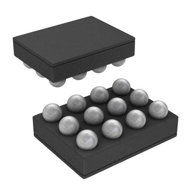
| 产品图片 |
|
| 产品型号 | LX27901ID-TR |
| rohs | 无铅 / 符合限制有害物质指令(RoHS)规范要求 |
| 产品系列 | - |
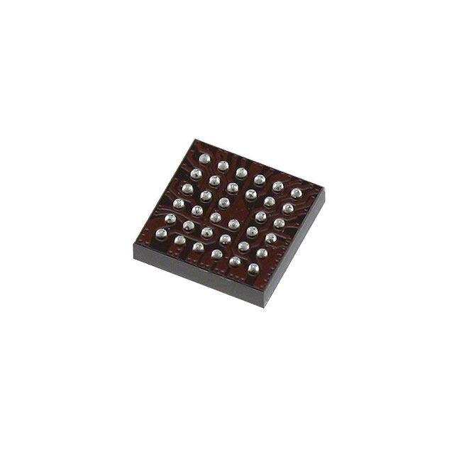
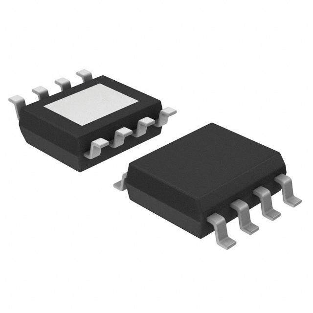
| 供应商器件封装 | 16-SOIC |
| 其它名称 | LX27901ID-TRDKR |
| 内部驱动器 | 无 |
| 包装 | Digi-Reel® |
| 安装类型 | 表面贴装 |
| 封装/外壳 | 16-SOIC(0.154",3.90mm 宽) |
| 工作温度 | -40°C ~ 85°C |
| 恒压 | - |
| 恒流 | - |
| 拓扑 | PWM |
| 标准包装 | 1 |
| 电压-电源 | 7.5 V ~ 27 V |
| 电压-输出 | - |
| 类型-初级 | 背光 |
| 类型-次级 | - |
| 输出数 | 2 |
| 频率 | 1MHz |


- 商务部:美国ITC正式对集成电路等产品启动337调查
- 曝三星4nm工艺存在良率问题 高通将骁龙8 Gen1或转产台积电
- 太阳诱电将投资9.5亿元在常州建新厂生产MLCC 预计2023年完工
- 英特尔发布欧洲新工厂建设计划 深化IDM 2.0 战略
- 台积电先进制程称霸业界 有大客户加持明年业绩稳了
- 达到5530亿美元!SIA预计今年全球半导体销售额将创下新高
- 英特尔拟将自动驾驶子公司Mobileye上市 估值或超500亿美元
- 三星加码芯片和SET,合并消费电子和移动部门,撤换高东真等 CEO
- 三星电子宣布重大人事变动 还合并消费电子和移动部门
- 海关总署:前11个月进口集成电路产品价值2.52万亿元 增长14.8%
_renders/IS31FL3728-QFLS2-TR.jpg)


PDF Datasheet 数据手册内容提取
LX27901 Multipurpose High Performance LED Controller ® TM PRELIMINARY DATASHEET W W DESCRIPTION KEY FEATURES W The LX27901 is an extremely The LX27901 is designed to operate LLC, PWM and proprietary M. versatile high-performance with Microsemi’s proprietary synchronous modes to drive the LED W ic r controller for driving LEDs from the lossless (magnetic) current strings W o s HVDC (output) rail of a standard balancing schemes. LED strings can be dimmed by PWM W e or analog methods M. m PFC front-end. Proprietary algorithm to provide ic i .C The controller also provides a accurate brightness control at high ro O The controller allows the user to proprietary synchronous regulation efficiency over wide dimming duty s M cycle range e utilize three different converter function to allow the user to control m drive schemes, LLC (resonant), the LED current and dimming from Accurate parallel LED strings current i . matching using Microsemi’s patented C conventional PWM control, and an unregulated switching power non-dissipative current-balancing O Microsemi’s proprietary supply source, to minimize the technology M synchronous scheme, all selectable number of power conversion stages Robust protection from open or by the multi-function ENABLE pin. and the associated losses and shorted LED conditions component costs. Dedicated fault indication In non-resonant mode, the 0.8A Source & Sink Drive Capability controller provides two 180° phase- A versatile set of system monitoring On Chip 5.25V Regulator shifted pulse-width modulated drive and protection functions are Direct connection to input voltage signals for implementing various incorporated in the LX27901 design rail up to 27V two-switch DC-DC converter to provide reliable protection of the LLC max operating frequency to 1 MHz, PWM to 150 kHz topologies, such a half-bridge and device and the system. These can asymmetrical forward converter. It account for shorted and open LED Synchronous regulation function to minimize power conversion stage can also be used for one-switch strings for example. RoHS compliant & halogen Free topologies. Three input pins, ISNS, VSNS and UVS/SYN are assigned to support APPLICATIONS Direct PWM input dimming regulation and protection. A LL LCD LED Backlight TV operation can be realized by dedicated fault indication pin allows XX LCD LED Backlight Monitors inputting a suitable dimming pulse the user to generate a direct fault 22 Other LED Backlight Systems train to the DIM pin. The LX27901 report to the system and configure 33 supports analog LED current control addition protection features with 00 44 utilizing the BRTA pin for setting the simple external circuits. analog LED current. The device is available in 16 lead SOIC surface mount package in the industrial temperature range. In addition, a proprietary dimming algorithm ACU_BRITE® is incorporated. The controller Refer to the Application Note titled integrates the pulsed LED current “Some Proprietary LED Current LL and compares it with a reference for Balancing Techniques”. XX very accurate brightness control 22 irrespective of duty cycle. 77 99 00 11 Page 1 Copyright 2012 Microsemi Rev. 0.3_03-27-2013 Analog Mixed Signal Group One Enterprise Aliso Viejo, CA 92656 USA
LX27901 Multipurpose High Performance LED Controller ® TM PRELIMINARY DATASHEET W W IMPORTANT: For the most current data, consult MICROSEMI’s website: http://www.microsemi.com W M. i W c r W o s PACKAGE ORDER INFO THERMAL DATA W e D Plastic SOIC 16 Pin = 82.2 C/W M. m TA (C) RoHS Compliant / Pb-free THERMAL RESIJSATANCE-JUNCTION TO AMBIENT icr i .C o O Junction Temperature Calculation: TJ = TA + (PD x JA). s M -40 to +85 LX27901ID The JA numbers are guidelines for the thermal em performance of the device/pc-board system. All of the Note: Available in Tape & R e(ie.el.. LAXp2p7e9n0d1 tIhDe- TleRtt)e rs “TR” to the part number. awbiothv e4 -alsasyuemr pe cnbo b aomarbdi.e nt airflow. JA number above is i .C O M AABSOLUTE MAXIMUM RATINGS PACKAGE PIN OUT Supply Input Voltage, VIN ............................................................................... 0.3V to 36V VIN VDD Signal Outputs, VDD, AOUT, BOUT, C_OUT ..............................................-0.3V to 6.5V Signal Inputs, C_R, BRTA .................................................................. -0.3V to VDD+0.3V ENABLE AOUT Signal Inputs, ENABLE, DIM, ISNS, VSNS, UVS/SYN ................... -0.3V to VDD+0.3V SMSPL iteegoaaanxrkdaia mgPTl eaOeu cTmmuketpa pmJgeuurepnta seStc ruCtoairoltOedun. erM (erTS PRReo,mlea dSfnpelSgoerTeirwna ./.B gt.Tu. C.1re.e.0mO. .. ..sMp..e..e..c,..r ..oaF....ntA..u..d..rU..se..).. L ...(...4...T...0... .... ....s........e....c........o........n........d........s........ ....m............a....x........i....m............u............m............ ....e....x........p........o........s........u........r....e.. .-...)6 ..- ...05..........3...C...V... ...t... o...t...o 1231 V56050000D°°°DCCCC BSCRDS_TITRMA/ xxxxLX27901ID MSC BGCON_OUDUTT COMP Notes: Exceeding these ratings could cause damage to the device. All voltages are with respect to BCOM GND. Currents are positive into, negative out of specified terminal. These are stress ratings FAULT ISNS only and functional operation of the device at these or any other conditions beyond those UVS/ indicated under “Recommended Operating Conditions” are not implied. Exposure to VSNS “Absolute Maximum Ratings” for extended periods may affect device reliability. SYN LX27901ID D PACKAGE LL (Top View) XX RoHS / Pb-free Matte Tin Pin Finish 22 33 ELECTRICAL CHARACTERISTICS 00 44 Unless otherwise listed, the following specifications apply over the operating ambient temperature of -40°C < Temp < 85°C, and VIN = 7.5V to 27V, except where otherwise noted and the following test conditions: VIN = 12V, C = 330pF, R = 15K C_R C_R Parameters Symbol Test Conditions/Comments MIN TYP MAX Units Power Controller Input Voltage VIN 7.5 27 V 1µF bypass cap on VDD pin, Controller Operating Voltage VDD 5.0 5.25 5.5 V IVDD = 0 to 5mA LL Power Supply Input Current IIN AOUT, BOUT = no load, VDD = no load 7 10 mA XX Sleep Mode Current IDD VIN = 24V, V < 0.8V 200 400 µA 22 SLEEP ENABLE 77 VDD Off Voltage ENABLE < 0.8V 0.1 V 99 00 Enable 11 ENABLE On EN 1.7 V H Page 2 Copyright 2012 Microsemi Rev. 0.3_03-27-2013 Analog Mixed Signal Group One Enterprise Aliso Viejo, CA 92656 USA
LX27901 Multipurpose High Performance LED Controller ® TM PRELIMINARY DATASHEET W ELECTRICAL CHARACTERISTICS W W Unless otherwise listed, the following specifications apply over the operating ambient temperature of -40°C < Temp < 85°C, and VIN = 7.5V to 27V, except where . M otherwise noted and the following test conditions: VIN = 12V, C = 330pF, R = 15K C_R C_R i W c Parameters Symbol Test Conditions/Comments MIN TYP MAX Units r W o s Shut Down EN 0.8 V W e L . m LLC Resonant Mode M Threshold VLLCTH LLC resonant drive mode, VDD = 5.25V 2 3 V ic i .C r PWM Switching Mode o O V PWM switching drive mode, VDD = 5.25V 3 4 V Threshold PWMTH s M e Synchronous LED Drive Mode m V Synchronous LED drive mode, VDD = 5.25V 4 VDD V Threshold SYN i . Input High Current EN ENABLE = 2V 10 µA C IIH O M Input Low Current EN 0V < V < 0.8V 5 µA IIL ENABLE Under Voltage Lockout VDD Startup Threshold VDD Rising Threshold. 4.35 4.6 4.8 V UVLOR VDD UVLO Threshold VDD Falling Threshold. 4.0 4.2 4.45 V UVLOF VDD UVLO Hysteresis VDD 0.4 V UVLOH Output Output Resistance R I , AOUT and BOUT, T = 25°C 5 6 Ω SINK SINK A Output Resistance R I , AOUT and BOUT, T = 25°C 5 6 Ω SOURCE SOURCE A Dead Time OUT T = 25°C, at full duty 250 330 410 ns DT A C_OUT Output Resistance R Source and sink 15 20 Ω C_OUT Switching Frequency Oscillator LL Switching Frequency OSCIN TA = 25°C, Frequency of AOUT, BOUT in PWM 128.8 140 151.2 kHz XX Tolerance PWM mode, C =330pF, R = 15K. C_R C_R 22 T = 25°C, Frequency of AOUT, BOUT in LLC Max Oscillator Frequency OSCMAX_LLC mAode, C =330pF, R = 15K. 1 MHz 33 C_R C_R 00 LLC Frequency Control Current Source VENABLE < 2.8V 0 200 µA 44 Ramp Valley Voltage OSCVV 0.5 V Ramp Peak Voltage OSCPV 2.5 V Ratio of UVS/SYN input over C_R oscillator Synchronization Range 1.05 3 Ratio free run frequency LED Dimming Control ISNS Reference ISNS TA = 25°C, input, Corresponds to 2V after 414.6 421 426.4 mV LL REF 4.75X internal amplifier. XX ISNS Linear Input Range Linear operation range for internal circuit 800 mV 22 4.75 times of ISNS signal. Input outside the 77 BRTA Input Range range is clamped at upper or lower limit 0.5 2.0 V 99 internally. 00 11 Pre-Amplifier Gain K 4.75 PRAMP Error Amp Output Capacity Source and Sink 100 µA Page 3 Copyright 2012 Microsemi Rev. 0.3_03-27-2013 Analog Mixed Signal Group One Enterprise Aliso Viejo, CA 92656 USA
LX27901 Multipurpose High Performance LED Controller ® TM PRELIMINARY DATASHEET W ELECTRICAL CHARACTERISTICS W W Unless otherwise listed, the following specifications apply over the operating ambient temperature of -40°C < Temp < 85°C, and VIN = 7.5V to 27V, except where . M otherwise noted and the following test conditions: VIN = 12V, C = 330pF, R = 15K C_R C_R i W c Parameters Symbol Test Conditions/Comments MIN TYP MAX Units r W o s DIM Input Voltage Range V Effective for duty from 0 to 100% 0.5 2.0 V W e DIM . m Voltage level of FAULT pin, in ACU_BRITE M PThWreMs hDoimld ming Mode Control VPDMODETH PcoWnvMe ndtiimonmailn Pg WmMod dei mwmheinng b meloodwe t hwrheesnh old; in 2.8 3.0 3.2 V icro i .CO above threshold. s M e Fault Monitoring and Protection m i . VSNS Threshold VSNS Fault when above the threshold 1.8 2.0 2.2 V C TH O VSNS Clamping Current I Pull down source at COMP pin 160 µA M Source CLAMP Fault when below the threshold, positive and UVS/SYN Threshold UVS/SYN 0.35 0.4 0.45 V TH negative input Functional operation range, positive and UVS/SYN Input Range V -0.5 4 V UVS/SYN negative input ISNS Fault Threshold V Fault when below the threshold 85 100 115 mV ISNSTH Over Current Threshold OC Upper threshold for ISNS input 550 600 650 mV TH Short Circuit Threshold SC Upper threshold for ISNS input 870 930 990 mV TH Fault Count FC At clock frequency of AOUT, BOUT 256 Count Interval for resetting fault counter, At clock Fault reset Interval F 32768 Count RESET frequency of AOUT, BOUT Fault Output Sinking Capacity F VFAULT ≤ 0.8V, TA = 25°C 4 6 mA SINK Fault Output Open Impedance R When in open state 5 MΩ F Bias & References LL XX Internal Master Reference VREF 1.2 V Voltage 22 33 Soft Start Charging Source I C_B Charging source at start up 2 µA SSC 00 Power-Up Sequencing 44 Power On Reset Time TPOR After UVLO of VDD released 50 µs Start up Time Out TSTART After POR 32768 Count LL XX FUNCTIONAL PIN DESCRIPTION Name Pin # Description 22 77 Input voltage pin. A built-in regulator is connected to this pin to step down the input voltage to the internal 99 operating voltage VDD. This pin can accept input voltage from 10V to 27V to provide the flexibility of 00 VIN 1 interfacing with either 12V or 24V system supply. A low ESR decoupling capacitor of not less than 1µF 11 should be connected from this pin to GND with low impedance traces. ENABLE 2 Enable pin to control the on/off operation of the controller. A logic low signal <0.8V on this pin sets the Page 4 Copyright 2012 Microsemi Rev. 0.3_03-27-2013 Analog Mixed Signal Group One Enterprise Aliso Viejo, CA 92656 USA
LX27901 Multipurpose High Performance LED Controller ® TM PRELIMINARY DATASHEET W FUNCTIONAL PIN DESCRIPTION W W Name Pin # Description . controller in sleep mode to save energy, and a signal > 2V activates the controller operation. The DC signal M level on this pin also sets the drive mode of the controller. When 2V<VENABLE<3V the AOUT, BOUT signals W ic are set in LLC resonant drive mode. When 3V<V <4V the controller drives the power converter in r ENABLE W o normal PWM drive mode; and when VENABLE >4V the controller is set in synchronous LED drive mode. W se . m M C_R 3 Ccaopnavceirtoter rc oonpneeracttiendg frforemq utheinsc pyi np troo ggrraomunmdi ndge tetermrminineasl .t h eA s wpiutcllh-uinpg rferesqisutoern cfyro omf ththei sin vpeinr tetor. VDD and a ic i .C r o O s M Terminal for programming the analog LED current setting. An analog signal is accepted from this pin to set BRTA 4 e the reference level for the LED current control loop. m i . PWM dimming control input. V > 2V sets the dimming operation in continuous analog mode. A PWM C DIM O DIM 5 signal of low level <0.5V and high level > 2V will force the PWM dimming operation to follow the PWM M signal directly. Input level <0.5V will stop the controller output. For PWM dimming brightness compensation and soft start. The elapsed dimming demand and the accumulated LED current over the active dimming period are compared at this pin. The comparison result is used to control the LED light output to exactly match the dimming demand with compensation for the distortion of the LED current during dimming operation. At start up this pin is connected to a 2µA charging SST/BCOM 6 current source to control the soft start process. An internal active pull down circuit is connected from this pin to COMP to force the COMP voltage rise slowly with the charge of the capacitor at this pin. Soft start completes when the voltage rises to 2.5V and the control enters normal operation mode. The 2µA charging source and the COMP pull down circuit is disconnected then, and this pin is connected to the brightness compensation circuit. Fault indication pin with open drain output. Internally pulled down when an open LED string, severely shorted LED string, over voltage of the LED strings, or over current occurs. Once latched, the fault signal can only be reset by ENABLE or power recycling. The voltage level at this pin during normal operation also sets the operation mode of dimming control. When the voltage is above 3V the COMP signal is turned on FAULT 7 and off by the digital dimming control signal and AOUT, BOUT and C_OUT are turned on and off accordingly by the COMP signal. When the voltage at the FAULT pin is below 3V the COMP signal is turned on and off by the control signal from the ACU_BRITE dimming control algorithm, and AOUT, BOUT LL and C_OUT are turned on and off accordingly by the COMP signal. The voltage level of this pin during XX normal operation can be set by an external resistive divider. 22 Sense for under voltage conditions. A threshold of 0.4V is set internally to compare the sense feedback 33 signal to this pin when the LED strings are on. A fault will be declared if the sensed signal stays below the 00 44 threshold over certain counts set by the internal circuitry. LED string current and voltage sense signals can UVS/SYN 8 be fed to this pin to detect open or short string conditions. When the controller is set in synchronous regulation mode UVS/SYN will receive the synchronization signal from the power supply to synchronize the switching frequency of AOUT and BOUT. An internal rectifier circuit is included to allow an AC input signal to be connected to this pin directly. Voltage sense input pin. The voltage signal on this pin feeds the over voltage detection circuit. A threshold of 2V is set internally for fault detection. When the voltage sense signal reaches the threshold of 2V, a VSNS 9 clamping current source will be activated to pull down COMP signal to limit the sensed voltage. In the meanwhile, the fault monitoring circuit will start counting the accumulated fault duration and set up the fault LL flag when the fault count reaches pre-determined counts. XX Current sense input pin. A full wave rectifier circuit is built in to allow AC input to this pin. The regulation 22 point at this pin is 421mV which is amplified by 4.75 times and then fed to the error amplifier to compare 77 with a reference signal of 2V to regulate the LED current. This signal is also used to detect open LED, over 99 ISNS 10 current and short circuit conditions. The threshold for open LED is 100mV, the threshold of over current is 00 11 600mV, and the threshold for short circuit is 930mV. A fault flag will be declared if ISNS signal stays below 100mV or above 600mV over defined counts, and the operation will be cut off immediately when ISNS signal goes above 930mV. Page 5 Copyright 2012 Microsemi Rev. 0.3_03-27-2013 Analog Mixed Signal Group One Enterprise Aliso Viejo, CA 92656 USA
LX27901 Multipurpose High Performance LED Controller ® TM PRELIMINARY DATASHEET W FUNCTIONAL PIN DESCRIPTION W W Name Pin # Description . M Output of the error amplifier. The error amplifier is a GM type that provides robust control behavior and i COMP 11 simple compensation. The signal on this pin feeds to the PWM modulation circuit to control the drive output W c r to regulate the LED current. At start up the voltage of this pin is controlled by the soft start circuit. W o s W e Gate signal to drive an additional MOSFET for LED current regulation. The signal is synchronized with the . m M C_OUT 12 Csy_nRc horoscniolluasto rr efgreuqlauteionnc ym aondde si sa nleda dtrinagili negd geed gme omduoldauteladt ebdy inth eP WouMtp huat lof-fb rthideg ee rdrorirv ea mmpolidfiee.r iTn hLisL Csi gannadl ic i .C r can be used in combination with AOUT and BOUT to extend the regulation range in LLC operation mode or o O provide additional driving capabilities in synchronous regulation mode. s M e m Gate drive outputs. These driver outputs are capable of providing 0.8A source and sink current at nominal operating voltage. Dead time is inserted to prevent possible shoot through at full duty cycle. Internal pull i . C down resistors of 20kΩ are provided at each of these pins. When the controller is in LLC mode AOUT and O BOUT are driven to maximum duty cycle (50%), and their switching frequency varies with the COMP signal M level. When the controller is in PWM mode these two outputs generate standard (non-resonant) AOUT 15 synchronous pulse-width modulated signals at fixed frequency. When the controller is in synchronous LED drive mode, UVS/SYN receives the synchronization signal, AOUT outputs an N-channel FET drive signal BOUT 13 synchronized with the rising edge of the (UVS/SYN) sync input signal, and BOUT outputs a P-channel FET drive signal synchronized with the falling edge cycle of the (UVS/SYN) sync input signal. Together they drive the external power devices to control the LED current directly (synchronous topology). This is different from the PWM mode, because the pulse-width of AOUT and BOUT signals is leading edge modulated in the synchronous drive mode. Ground return of the on chip circuit. It is important to provide a low impedance ground plane to this pin and the signal control circuitry in PCB layout, and not let the ground return current of the inverter power circuit GND 14 flow through the signal ground plane. Low ESR bypass capacitors for VDD and VDD should be connected with lowest possible impedance to this pin through the signal ground plane. The operating voltage of the IC. A built-in regulator supplies a regulated 5.25V derived from VIN supply to VDD 16 this pin. A low ESR decoupling capacitor of not less than 1µF should be connected from this pin to GND with low impedance traces. LL XX 22 33 00 44 LL XX 22 77 99 00 11 Page 6 Copyright 2012 Microsemi Rev. 0.3_03-27-2013 Analog Mixed Signal Group One Enterprise Aliso Viejo, CA 92656 USA
LX27901 Multipurpose High Performance LED Controller ® TM PRELIMINARY DATASHEET W W W FUNCTIONAL BLOCK DIAGRAM . M i W c r W o s W e . m M ic i .C r o O VIN REGVUDLDATOR ULVPOLOGORIC & INITIALLOAGZIACTION AOUT sem M i . VDD C MODE DRIVER O SELECTION BOUT ENABLE LOGIC PWM PWM SIGNAL BLOCK M MODULATION PHASE SIGNAL C_OUT FREQUENCY SYNC LOGIC CONTROL SYNC RAMP POR RESET OSCILLATOR GENERATION START UP & C_R CIRCUIT RESET TIMER V Q CLOCK _ COMP D Q BRTA + EA 0.5V +- - PWM ISNS FWARM &P 5X IS COI_NSTNRSOL DIMMING CLOCK LL CONTROL RESET XX + 3.0V - FAULT 22 SST/ SAOCFUT_ SBTRAITRET + FAULT TIMING PWM DIMMING 33 BCOM CONTROL 4.65V - CONTROL CONTROL 00 IS - 44 0.5V + SSETQ 0.4V + RCLRQ POR - POR 2.0V - 3.0V + + FAULT - DIM + 1.5V - VSNS LL SYNC POINT FULL WAVE UVS/ XX SYNC DETECTION RECTIFIER SYN 22 GND 77 LX27901 99 00 11 Figure 1. LX27901 Functional Block Diagram. Page 7 Copyright 2012 Microsemi Rev. 0.3_03-27-2013 Analog Mixed Signal Group One Enterprise Aliso Viejo, CA 92656 USA
LX27901 Multipurpose High Performance LED Controller ® TM PRELIMINARY DATASHEET W W W . TYPICAL PERFORMANCE CHARACTERISTICS M i W c r W o s W e . m M ic i .C r o O s M e m i . C O M Figure 2 Figure 3 LL XX 22 33 00 44 Figure 4 Figure 5 LL XX 22 77 99 00 11 Page 8 Copyright 2012 Microsemi Rev. 0.3_03-27-2013 Analog Mixed Signal Group One Enterprise Aliso Viejo, CA 92656 USA
LX27901 Multipurpose High Performance LED Controller ® TM PRELIMINARY DATASHEET W W W . M i W c r W o s W e . m M ic i .C r o O s M e m i . C O M Figure 6 Figure 7 TYPICAL PERFORMANCE CHARACTERISTICS STARTUP WITH ENABLE LLC MODE OUTPUT TIMING SYNC MODE LL XX 22 33 00 44 Figure 8 Figure 9 Channel 1: BOUT, Channel 2: I_LED Channel 1: AOUT, Channel 2: BOUT Channel 3: AOUT, Channel 4: ENABLE Channel 3: COUT, Channel 4: UVS LL DIMMING SYNC MODE VSNS OV PROTECTION MODE XX 22 77 99 00 11 Page 9 Copyright 2012 Microsemi Rev. 0.3_03-27-2013 Analog Mixed Signal Group One Enterprise Aliso Viejo, CA 92656 USA
LX27901 Multipurpose High Performance LED Controller ® TM PRELIMINARY DATASHEET W W W . M i W c r W o s W e . m M ic i .C r o O s M e m i . C O M Figure 10 Figure 11 Channel 1: AOUT, Channel 2: BOUT Channel 1: AOUT, Channel 2: C_R Channel 3: COUT, Channel 4: UVS Channel 3: FAULT, Channel 4: VSNS LL XX 22 33 00 44 LL XX 22 77 99 00 11 Page 10 Copyright 2012 Microsemi Rev. 0.3_03-27-2013 Analog Mixed Signal Group One Enterprise Aliso Viejo, CA 92656 USA
LX27901 Multipurpose High Performance LED Controller ® TM PRELIMINARY DATASHEET W W TYPICAL PERFORMANCE CHARACTERISTICS W . M LLC DIMMING MODE PWM DIMMING MODE i W c r W o s W e . m M ic i .C r o O s M e m i . C O M Figure 12 Figure 13 Channel 1: AOUT, Channel 2: BOUT Channel 1: AOUT, Channel 2: BOUT Channel 3: COUT, Channel 4: C_R Channel 3: COUT, Channel 4: C_R ACU_BRITE DIMMING MODE DIRECT PWM DIMMING MODE LL XX 22 33 00 44 LL XX Figure 14 Figure 15 22 Channel 1: AOUT, Channel 2: BOUT Channel 1: AOUT, Channel 2: BOUT 77 Channel 3: PWM_DIM, Channel 4: ILED Channel 3: PWM_DIM, Channel 4: ILED 99 00 11 Page 11 Copyright 2012 Microsemi Rev. 0.3_03-27-2013 Analog Mixed Signal Group One Enterprise Aliso Viejo, CA 92656 USA
LX27901 Multipurpose High Performance LED Controller ® TM PRELIMINARY DATASHEET W W TYPICAL PERFORMANCE CHARACTERISTICS W . M ACU_BRITE DIMMING MODE DIRECT PWM DIMMING MODE i W c r W o s W e . m M ic i .C r o O s M e m i . C O M Figure 16 Figure 17 Channel 1: AOUT, Channel 2: BOUT Channel 1: AOUT, Channel 2: BOUT Channel 3: PWM_DIM, Channel 4: ILED Channel 3: PWM_DIM, Channel 4: ILED LL XX 22 33 00 44 LL XX 22 77 99 00 11 Page 12 Copyright 2012 Microsemi Rev. 0.3_03-27-2013 Analog Mixed Signal Group One Enterprise Aliso Viejo, CA 92656 USA
LX27901 Multipurpose High Performance LED Controller ® TM PRELIMINARY DATASHEET W W TYPICAL APPLICATION SCHEMATIC W . M W ic r W o s W e . m M ic i .C r o O s M e VDC+ m i . C C25 1BX14 O R14R7 Q1 M 3 5 3 1 +C471u/450V 9 D1 BAS21 C3 0.01U/450V 1 TX1 5 2 10 4 4 67 2 3 C2 R2 4R7 Q2 C26 1BX24 1uF 3 1 D2 BAS21 3 5 PGND D1 D2 D3 D4 +12V R337 C411uF VDD 200K C401uF LED1 LED2 LED3 LED4 R338 LED LED R3 R4 R7 U1 2K LED LED 5.1K 51K 10K 1 VIN VDD 16 R186 C21 C22 C23 C24 ENABLE 2 ENABLE AOUT 15 3 C_R GND 14 2K LED LED PWFAA_MDU_ILDMTIM RR224522KK 5467 DBSFARSIMUTT/ALBTCOM CCB_IOOOSMNUUPSTT 11110123 C144.7n D7132 BAV7R015 2K LED LED R106K9 1R02K31 LXLX 8 UVS/SYN VSNS 9 D8 22 1R05K C1060p 5R.61K C2270p 0.01u C0.91u C1n1F0 LX27901 C1n1F1 C0.1021u C1n1F3 5R.81K R0.148R5 R171K 3BAV70 21 R184 R232 3030 3K 3K 44 LL XX Figure 18 22 77 LLC CONTROL MODE 99 00 (The component values are for reference only, modifications may be necessary for a particular application requirement.) 11 Page 13 Copyright 2012 Microsemi Rev. 0.3_03-27-2013 Analog Mixed Signal Group One Enterprise Aliso Viejo, CA 92656 USA
LX27901 Multipurpose High Performance LED Controller ® TM PRELIMINARY DATASHEET W W TYPICAL APPLICATION SCHEMATIC W . M W ic r W o s W e . m M ic i .C r o O VDC+ s M e Q1 m TX1 11 D1A 1BX16 i .C C3 1 10 D1B 2 5 O 3 4 9 M +C1 8 D2A Q2 2 7 6 D2B D3 VDC1 PGND D4 DRIVE CONTROL FOR VDC1 R92 R95 100K 100K LED1 LED2 +12V VDD R93 R96 C321uF 2K 2K C311uF C11 C12 R3 R4 U1 5.1K 51K 1 VIN VDD 16 ENABLE 2 ENABLE AOUT 15 1 2 BAV70 LL D5 3 C_R GND 14 XX A_DIM 4 BRTA BOUT 13 3 PWM_DIM R242K 5 DIM C_OUT 12 22 6 SST/BCOM COMP 11 C144.7n Q3 33 FAULT R252K 7 FAULT ISNS 10 R15 1K 00 8 UVS/SYN VSNS 9 44 LX27901 R5 R8 C6 C9 R6 20K C13 C7 C11 C12 R100 10K 100p 220p 0.1u C10 R7 1nF 0.01u 1nF 5.1K 0.4R 1nF 10K LL XX 22 Figure 19 77 SYNCHRONOUS REGULATION MODE 99 00 11 (The component values are for reference only, modifications may be necessary for a particular application requirement.) Page 14 Copyright 2012 Microsemi Rev. 0.3_03-27-2013 Analog Mixed Signal Group One Enterprise Aliso Viejo, CA 92656 USA
LX27901 Multipurpose High Performance LED Controller ® TM PRELIMINARY DATASHEET W W OOPERATION DOPERATION DESCRIPTION ESCRIPTION W . INTRODUCTION minimizing the power consumption at sleep mode. An M UVLO circuit is employed to monitor the VDD voltage. W ic r This section describes the operation of LX27901 LED The UVLO circuit releases the lock out function when W o s drive controller. LX27901 is primarily designed for LIPS VDD reaches its rising threshold and initiates the Power W e power systems for LED backlit LCD TV and other large On Reset (POR) signal. . m M screen CCFL backlight applications that addresses the ic i .C need to drive a half bridge or full bridge inverter stage The POR signal initializes the whole control circuitry by r o O from the 400V PFC output across the safety isolation resetting the counters, registers, fault latch, setting the s M barrier. It provides an optimized low cost solution for analog signals such as the SST/BCOM and C_B voltage to em such applications while providing a set of comprehensive pre-determined initial values, while holding off the i . control features to fully satisfy the technical output signals to pre-determined inactive states. After C O requirements. the preset delay time the POR signal is released and the M controller operation starts. 1. SYSTEM OVERVIEW 3. OSCILLATOR AND FREQUENCY CONTROL The system contains the following main function blocks: The system has a built in clock to control the switching frequency. A resistor and a capacitor are required, connected between VDD and C_R pin and from C_R pin to Power and Start-Up Logic ground respectively to set the oscillating frequency. A Oscillator and Frequency Control Circuit controlled charging current source is also provided Regulation Control Circuit internally to the C_R pin to adjust the oscillator Dimming Control Circuit frequency when the ENABLE voltage level is set in LLC Drive Control Circuitry resonance control mode. When the ENABLE voltage Fault Detection and Protection Circuitry level is set in PWM mode, the current source is disconnected and the oscillator returns to the free run The power and start-up logic provides regulated power frequency set by the external RC components. to the on chip circuitry and controls the start-up sequencing, power on reset, and soft start operation etc. 4. REGULATION CONTROL The oscillator and frequency logic generates the clock LL signals for the LLC and PWM operation and timing for The regulation circuit controls the LED current through XX the operation and protection. The regulation and closed loop regulation. The LED current is sensed and 22 dimming control logic handles the LED current fed to the ISNS pin as a feedback signal where it is 33 regulation and dimming control operation with regulated by an internal transconductance error 00 Microsemi’s proprietary ACU_BRITE technology to amplifier to match the current reference threshold. This 44 provide accurate brightness control with non-dissipative controls the PWM drive of the external switching operation of the power devices. The drive control circuit MOSFETs of the power conversion circuit. The output of converts the PWM signal from the regulation and control the error amplifier, available on the COMP pin, allows the circuit to power drive signals to drive the external power user to adjust the control loop directly if desired. Three devices of the power supply and LED string control. The power supply control modes are incorporated into the fault detection and protection logic monitors the controller operation operation of the internal and external circuits and provides fault warning and protection for the system. LLC Resonant control Mode: In LLC resonant mode the LL PWM drive output signals AOUT and BOUT remain at full XX 2. POWER CONTROL AND START UP duty cycle (50%), and the output signal from the error 22 amplifier controls the internal charging current source at 77 The LX27901 has a built in regulator to step down the C_R pin to adjust the switching frequency of AOUT and 99 input voltage VIN to a regulated 5.25V supply VDD to BOUT to regulate the LED current. Note that in this mode 00 support the on chip circuitry. The regulator is controlled the operating frequency of the drive signals should be 11 by the ENABLE signal and is only activated when always higher than the resonance frequency. ENABLE voltage goes above its logic threshold, thus Page 15 Copyright 2012 Microsemi Rev. 0.3_03-27-2013 Analog Mixed Signal Group One Enterprise Aliso Viejo, CA 92656 USA
LX27901 Multipurpose High Performance LED Controller ® TM PRELIMINARY DATASHEET W W OOPERATION DOPERATION DESCRIPTION ESCRIPTION W . M SST/BCOM is fed to a comparator and compared with a PWM control Mode: The internal current source at C_R i pin is disconnected and AOUT and BOUT signals remain t2h.5reVs, hthoeld L lEeDve clu orfr e2n.5t Vis. t uWrnheedn oVnS,S Ta/nBCdO Mw ihse gnr Veater thains WW cro at the fixed frequency set by the RC components at C_R SST/BCOM s lower than 2.5V, the LED current is turned off. W e pin, and the LED current is regulated by adjusting the . m With such control mechanism the integration of the LED M p ulse width of the AOUT and BOUT signals. current always matches the integration of its reference ic i .C r over the digital dimming operation to yield an accurate o O Synchronous regulation Mode: The synchronization s M signal from the power supply is received from UVS/SYN brightness control. This feature essentially enables the e control of dimming operation by turning on and off the m pin and AOUT and BOUT output drive signals in synchronous with the synchronization signal to drive power supply directly without losing dimming accuracy, i .C instead of putting an additional control device in series respective external switches in series with the LED O with the LED string to control the LED on/off. The LED M strings to control the LED current. In this mode AOUT current distortion at the rising and falling edge of the and BOUT are leading edge modulated PWM drive digital dimming operation is accurately compensated by signals controlled by the closed current loop from ISNS the dimming duty adjustment, the no load power supply feedback. The three control modes are selectable by the losses at LED off state are eliminated, and the serial voltage level of ENABLE signal. When 2V<VENABLE<3V the control device is removed. controller is in LLC resonant drive mode; when 3V<V <4V the controller drives the power supply in ENABLE 6. DRIVE CONTROL CIRCUIT PWM drive mode; and when V >4Vthe controller ENABLE drives the external device in synchronous regulation The drive control circuit converts the PWM signal mode. from the regulation and control circuit to the drive output signals AOUT, BOUT and C_OUT to drive the 5. DIMMING CONTROL external power devices for the power supply and LED string control. The signals from AOUT and BOUT are The LX27901 supports external burst dimming and 180° out of phase. When the controller is in LLC analog dimming functions. In external digital dimming resonant mode AOUT and BOUT remain at full duty, and mode a dimming pulse train is supplied to DIM pin and their switching frequency varies with the COMP signal the dimming operation follows the input pulse train LL level to adjust the power supply output. When the directly. It is recommended that the high state of the controller is in the PWM control mode AOUT and BOUT XX pulse train should be higher than 2V and the low state remain at a fixed switching frequency but their duty 22 should be lower than 0.5V. This signal is compared with cycle varies with the COMP signal level. When in 33 an internal DC level of 1.5V to generate an internal PWM 00 synchronous regulation mode AOUT outputs a NFET pulse train to control the burst dimming operation. 44 drive signal in synchronous with the positive cycle of the A unique feature called ACU_BRITE is incorporated to synchronization signal from UVS/SYN pin, and BOUT compensate the LED current error by digital dimming outputs a PFET drive signal in synchronous with the duty adjustment. A capacitor from SST/BCOM pin to negative cycle of the synchronization signal from ground provides an integration function for such control. UVS/SYN to drive the external devices. In this mode the A controlled charging current source and a controlled AOUT and BOUT signal is a leading edge modulated discharging current source are connected internally to PWM signal with their falling edge in synchronous with the SST/BCOM pin. The charging current source is the zero crossing point of the synchronization signal to linearly proportional to the internal current regulation LL minimize their turn off transient and their pulse width is reference and turned on and off by the internal digital controlled by the closed current loop from ISNS XX dimming signal. The discharging current source is feedback. The driving capacity of AOUT and BOUT is 22 proportional to the ISNS signal at the same ratio as the 0.8A in both the sourcing and sinking mode. 77 charging source to the internal reference. At power on 99 reset the SST/BCOM capacitor is discharged to zero and 00 The signal from C_OUT provides the user additional the capacitor is used for soft start operation. When the 11 capacitor voltage reaches 2.5V it switches over to control for LED current regulation. The signal is in synchronous with the C_R oscillator frequency and is ACU_BRITE dimming control function. The voltage of Page 16 Copyright 2012 Microsemi Rev. 0.3_03-27-2013 Analog Mixed Signal Group One Enterprise Aliso Viejo, CA 92656 USA
LX27901 Multipurpose High Performance LED Controller ® TM PRELIMINARY DATASHEET W W OPERATION DESCRIPTION W . M leading edge modulated by the output of the error After the counter time out if ISNS signal is still below i amplifier in LLC and synchronous regulation modes, and 100mV while the LED is on, it indicates an open LED or W c r trailing edge modulated in PWM half bridge drive mode. power supply failure condition. A fault counter will start W o s This signal can be used in combination with AOUT and to count the fault. When the counter reaches the full W e . m BOUT to extend regulation range in LLC operation mode count of 256, a fault condition is confirmed and the M or provide additional driving capabilities in synchronous FAULT pin is pulled to low state to indicate a fault ic i .C regulation mode. condition. The fault counter is incremented by a clock at ro O the same frequency as AOUT, BOUT and reset s M e 7. SOFT START periodically at an interval of 32768 clock pulses. In m addition, during the interval if there is any single i . Soft start is accomplished by internal circuitry in occurrence of ISNS>100mV it will reset the fault counter C O combination with the SST/BCOM capacitor charging and the fault counting has to start all over again. Such M control. At power on the SST/BCOM capacitor is reset mechanism guarantees reliable fault detection and discharged to zero during POR. When the operation prevents noise triggered false fault reporting. The ISNS commences following POR the SST/BCOM pin is signal is also used to monitor over current and short disconnected from the dimming control circuit and a circuit conditions. A typical threshold of 600mV is set small soft start current source of 2 µA is turned on to for over current detection and a typical threshold of charge the SST/BCOM capacitor slowly. The voltage of 930mV is set for short circuit detection. The fault the SST/BCOM capacitor pulls down the COMP signal counter will start counting when ISNS>600mV occurs through the soft start circuit to force the V signal to and reports a fault when the counter reaches full count COMP rise slowly together with it. During this course the of 256. Periodical reset at every 32768 clock cycle voltage amplitude of SST/BCOM is monitored. When the interval is also employed for the fault counter. SST/BCOM signal rises to 2.5V, the soft start current source is turned off and the SST/BCOM pin switches over In addition, a time delay circuit, similar to a one shot, is to the internal dimming control circuit. The capacitor at employed to hold the over current status for about 50µs. SST/BCOM is charged and discharged by the ACU_BRITE The fault counter will be reset if the over current brightness compensation circuit and its voltage is condition does not persist when the elapsed holding compared with a 2.5V reference to turn on and off the time is over. When ISNS signal exceeds 930mV typically AOUT, BOUT and C_OUT signals while the COMP signal it will be recognized as a short circuit. The output signal LL resumes its role in the regulation function. During start will be shut off immediately with a fault flag raised. The XX up a timer-counter circuit is also furnished to monitor short circuit detection is active all the time after POR 22 the system operation. If the ISNS signal does not reach release. 33 100mV after the counter reaches the full count of 32k 00 44 (15 bit) clock cycles, the start-up is considered failed and The VSNS signal is used to limit and monitor over a fault flag is raised by pulling down the FAULT pin voltage condition. When the voltage sense signal reaches signal. the threshold of 2V, a clamping current source will be activated to pull down COMP signal to limit the sensed 3. 8. FAULT DETECTION AND PROTECTION voltage. In the meanwhile, the fault counter starts counting and reports fault condition when the counter The following system operating conditions are reaches full count. Periodical reset at every 32768 clock monitored with fault reporting and protection: cycle interval also applies to the VSNS fault counting. Open LED string, Short LED string, Power supply failure, Similarly a time delay circuit is also employed to hold the LL over voltage status for about 50µs. The fault counter will XX Over voltage and Over current. The above fault be reset if the over voltage condition does not persist 22 conditions are monitored from the ISNS, VSNS and when the elapsed holding time is over. In actual 77 UVS/SYN inputs. The ISNS signal is used to monitor open applications, if a balancer network is deployed in the 99 LED, power supply failure and over current conditions. 00 drive system, the signals from the secondary winding Open LED detection is disabled during start up until the 15 11 loop can also be fed to VSNS pin to detect open or short bit counter times out. LED fault. When a LED string is open or shorted, the Page 17 Copyright 2012 Microsemi Rev. 0.3_03-27-2013 Analog Mixed Signal Group One Enterprise Aliso Viejo, CA 92656 USA
LX27901 Multipurpose High Performance LED Controller ® TM PRELIMINARY DATASHEET W W OPERATION DESCRIPTION W . may result in overshoot, and the loop could become M voltage in the primary and secondary winding of the unstable. However as the capacitor value is increased it W ic associated balancer will rise dramatically, and such will reduce the gain and the loop response may be too W ro distinctive signal change can be readily used for open or slow. Therefore it is necessary to choose an optimal W se short LED detection with VSNS circuit. value, typical recommended values range from 1nF to M. m d e t e Tcthieo nU. V SA/ SthYrNe sshigonldal opfr o0v.4idVe sis f usretth einrt merenaanllsy f ofor rf atuhlet 1ap0pnlFic, abtuiot nsh roeuqludi rbeem aednjutss.t ed depending on the icro i .CO UVS/SYN signal. When UVS/SYN<0.4V occurs, the fault s M counter also starts counting and reports a fault condition e m when the counter reaches full count Periodical reset at VIN, VDD BYPASS CAPACITOR every 32k clock cycle interval also applies to the The LX27901 has internal Low Dropout Regulator to i .C UVS/SYN fault count. Similarly a time delay circuit is generate an accurate 5V supply for the internal control O M also employed to hold the over voltage status for about circuitry. In order to have stable operation, it is required 50µs. The fault counter will be reset if the over current to provide bypass capacitor with low ESR between both condition does not persist when the elapsed holding time VIN and VDD and ground. It is recommended to use a is over. capacitance of not less than 1F for VIN and 1uF for VDD. SETTING OPERATING FREQUENCY LAYOUT GUIDELINES The switching frequency of AOUT and BOUT is It is important to have a good PCB layout to achieve programmed with the external capacitor and resistor, stable operation. Especially, high voltage section and the power switching section of the circuit layout require R and C . C_R C_R particular attention. High voltage section layout also needs to be planned carefully to meet Safety 693000 requirement as well as proper isolation from the control f SW R C circuit. Following are guidelines for inverter PCB layout C_R C_R 1) Use a star-ground connection for analog and power ground. Analog ground should be isolated from LL f is the switching frequency in kHz, R is in kohms, power ground except one connection point, GND SW C_R XX and C is in pF. For most applications, lamp free run pin. C_R 22 frequency is set at less than 150kHz. Normally CC_R can 2) Route high speed digital signal traces away from 33 be chosen from 220pF to 470pF, and the value of R can sensitive analog signals. 00 C_R 3) Place decoupling cap as close to related pin as 44 also be used to adjust the frequency control range in LLC possible. mode. 4) Make shortest and direct connection from feedback sources. SETTING COMP PIN CAPACITOR 5) Keep short and wide for high current signal paths An external capacitor CCOMP is connected from this pin to especially ground. ground to adjust loop response of the inverter module. 6) Make trace as thick as possible The error amplifier is a GM type that provides robust 7) Route current sense and voltage divider traces away LL control behavior and simple compensation. The ideal from high voltage field. XX current error amplifier compensation depends on the dimming mode operation range. If minimal dimming is 22 77 required by the application the loop response can be 99 slower, but for wide range digital dimming it must be 00 fast enough to allow the lamp current to get to full 11 amplitude within a few current cycles. If value of C is small the gain will be increased and COMP Page 18 Copyright 2012 Microsemi Rev. 0.3_03-27-2013 Analog Mixed Signal Group One Enterprise Aliso Viejo, CA 92656 USA
LX27901 Multipurpose High Performance LED Controller ® TM PRELIMINARY DATASHEET W W W . M PACKAGE DIMENSIONS i W c r D 16-Pin Plastic Narrow Body SOIC W os W e MILLIMETERS INCHES M. m DIM MIN MAX MIN MAX ic i .C r D A 1.35 1.75 0.053 0.069 o O s M A1 0.10 0.25 0.004 0.010 e m A2 1.25 1.52 0.049 0.060 16 9 b 0.33 0.51 0.013 0.020 i .C H E c 0.19 0.25 0.007 0.010 O M 11 8 D 9.78 10.01 0.385 0.394 E 5.79 6.20 0.228 0.244 e 1.27 BSC 0.050 BSC L e B H 3.81 4.01 0.150 0.158 L 0.40 1.27 0.016 0.050 Θ 0 8 0 8 A2 A *LC 0.10 0.004 A1 c *Lead Coplanarity Note: 1. Controlled dimensions are in mm, inches are for reference only. 2. Dimensions do not include mold flash or protrusions; these shall not exceed 0.155mm (.006”) on any side. Lead dimension shall not include solder coverage. LL XX 22 33 00 44 LL XX 22 77 99 00 11 Page 19 Copyright 2012 Microsemi Rev. 0.3_03-27-2013 Analog Mixed Signal Group One Enterprise Aliso Viejo, CA 92656 USA
LX27901 Multipurpose High Performance LED Controller ® TM PRELIMINARY DATASHEET W W W NOTES . M i W c r W o s W e . m M ic i .C r o O s M e m i . C O M LL XX 22 33 00 44 LL XX 22 77 PRELIMINARY DATA – Information contained in this document is pre-production data 99 and is proprietary to Microsemi. It may not be modified in any way without the express 00 written consent of Microsemi. Product referred to herein is offered in pre-production form 11 only and may not have completed Microsemi’s Quality Assurance process for Release to Production. Microsemi reserves the right to change or discontinue this proposed product at any time. Page 20 Copyright 2012 Microsemi Rev. 0.3_03-27-2013 Analog Mixed Signal Group One Enterprise Aliso Viejo, CA 92656 USA