ICGOO在线商城 > 分立半导体产品 > 晶体管 - 双极 (BJT) - 单 > BUL128D-B

 Datasheet下载
- 型号: BUL128D-B
- 制造商: STMicroelectronics
- 库位|库存: xxxx|xxxx
- 要求:
| 数量阶梯 | 香港交货 | 国内含税 |
| +xxxx | $xxxx | ¥xxxx |
查看当月历史价格
查看今年历史价格
BUL128D-B产品简介:
ICGOO电子元器件商城为您提供BUL128D-B由STMicroelectronics设计生产,在icgoo商城现货销售,并且可以通过原厂、代理商等渠道进行代购。 BUL128D-B价格参考¥询价-¥询价。STMicroelectronicsBUL128D-B封装/规格:晶体管 - 双极 (BJT) - 单, 双极 (BJT) 晶体管 NPN 400V 4A 70W 通孔 TO-220AB。您可以下载BUL128D-B参考资料、Datasheet数据手册功能说明书,资料中有BUL128D-B 详细功能的应用电路图电压和使用方法及教程。
STMicroelectronics的BUL128D-B是一款双极型晶体管(BJT),属于单晶体管类别,广泛应用于多种电子电路中。以下是该型号的主要应用场景:

 1. 开关应用
   - BUL128D-B可以用作电子开关,适用于数字电路中的信号切换。例如,在继电器驱动、LED驱动或小型电机控制等场景中,它能够根据输入信号的高低电平控制负载的通断。

 2. 放大器设计
   - 作为一款双极型晶体管,BUL128D-B适合用于音频放大器、信号放大器和其他需要低噪声和高增益的放大电路中。它可以处理一定范围内的电流和电压,满足中小功率放大需求。

 3. 电源管理
   - 在一些简单的电源管理电路中,如线性稳压器或电流限制电路,BUL128D-B可以用来调节输出电流或电压,确保负载设备的安全运行。

 4. 传感器接口
   - 该晶体管可用于传感器信号的放大或转换。例如,在温度传感器、光电传感器或其他模拟信号输出的传感器中,BUL128D-B可以帮助增强信号强度,以便后续处理。

 5. 通信设备
   - 在低频通信电路中,BUL128D-B可以用作信号调制或解调的组件,支持数据传输的基本功能。

 6. 汽车电子
   - 由于其可靠性和稳定性,BUL128D-B也可用于汽车电子系统中的某些非关键部件,如指示灯控制、小型执行器驱动等。

 总结
BUL128D-B的主要特点包括耐压能力、电流承载能力和良好的频率响应,因此适用于中小型功率的开关和放大场景。在实际应用中,用户需要根据具体参数(如集电极-发射极电压、最大集电极电流等)选择合适的偏置条件和散热措施,以确保晶体管的稳定工作。
| 参数 | 数值 |
| 产品目录 | |
| 描述 | TRANS NPN HV FAST 400V TO-220 |
| 产品分类 | 晶体管(BJT) - 单路 |
| 品牌 | STMicroelectronics |
| 数据手册 | |
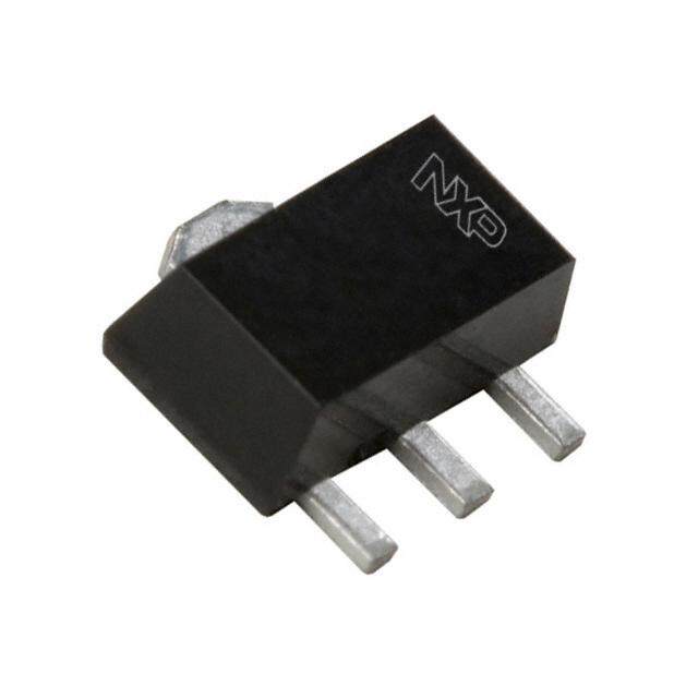
| 产品图片 |
|
| 产品型号 | BUL128D-B |
| rohs | 无铅 / 符合限制有害物质指令(RoHS)规范要求 |
| 产品系列 | - |
| 不同 Ib、Ic时的 Vce饱和值(最大值) | 500mV @ 1A,4A |
| 不同 Ic、Vce 时的DC电流增益(hFE)(最小值) | 12 @ 2A,5V |
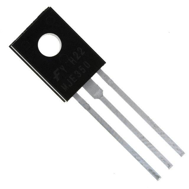
| 供应商器件封装 | TO-220AB |
| 其它名称 | 497-12755-5 |
| 其它有关文件 | http://www.st.com/web/catalog/sense_power/FM100/CL822/SC84/PF75092?referrer=70071840 |
| 功率-最大值 | 70W |
| 包装 | 管件 |
| 安装类型 | 通孔 |
| 封装/外壳 | TO-220-3 |
| 晶体管类型 | NPN |
| 标准包装 | 50 |
| 电压-集射极击穿(最大值) | 400V |
| 电流-集电极(Ic)(最大值) | 4A |
| 电流-集电极截止(最大值) | 250µA |
| 频率-跃迁 | - |


- 商务部:美国ITC正式对集成电路等产品启动337调查
- 曝三星4nm工艺存在良率问题 高通将骁龙8 Gen1或转产台积电
- 太阳诱电将投资9.5亿元在常州建新厂生产MLCC 预计2023年完工
- 英特尔发布欧洲新工厂建设计划 深化IDM 2.0 战略
- 台积电先进制程称霸业界 有大客户加持明年业绩稳了
- 达到5530亿美元!SIA预计今年全球半导体销售额将创下新高
- 英特尔拟将自动驾驶子公司Mobileye上市 估值或超500亿美元
- 三星加码芯片和SET,合并消费电子和移动部门,撤换高东真等 CEO
- 三星电子宣布重大人事变动 还合并消费电子和移动部门
- 海关总署:前11个月进口集成电路产品价值2.52万亿元 增长14.8%


PDF Datasheet 数据手册内容提取
BUL128D-B HIGH VOLTAGE FAST-SWITCHING NPN POWER TRANSISTOR n STMicroelectronics PREFERRED SALES Figure 1: Package TYPE n NPN TRANSISTOR n HIGH VOLTAGE CAPABILITY n LOW SPREAD OF DYNAMIC PARAMETERS n MINIMUM LOT-TO-LOT SPREAD FOR RELIABLE OPERATION n VERY HIGH SWITCHING SPEED n INTEGRATED ANTIPARALLEL COLLECTOR- EMITTER DIODE 3 2 1 APPLICATIONS TO-220 n ELECTRONIC BALLAST FOR FLUORESCENT LIGHTING n FLYBACK AND FORWARD SINGLE Figure 2: Internal Schematic Diagram TRANSISTOR LOW POWER CONVERTERS DESCRIPTION The device is manufactured using high voltage Multi Epitaxial Planar technology for high switching speeds and medium voltage capability. It uses a Cellular Emitter structure with planar edge termination to enhance switching speeds while maintaining the wide RBSOA. The device is designed for use in lighting applications and low cost switch-mode power supplies. Table 1: Order Codes Part Number Marking Package Packaging BUL128D-B BUL128D-B TO-220 Tube Table 2: Absolute Maximum Ratings Symbol Parameter Value Unit VCES Collector-Emitter Voltage (VBE = 0) 700 V VCEO Collector-Emitter Voltage (IB = 0) 400 V VEBO Emitter-Base Voltage V(BR)EBO V (I = 0, I = 2 A, t < 10 µs, T = 150 oC) C B p J IC Collector Current 4 A ICM Collector Peak Current (tp < 5ms) 8 A IB Base Current 2 A IBM Base Peak Current (tp < 5ms) 4 A Rev. 2 February 2005 1/8
BUL128D-B Symbol Parameter Value Unit Ptot Total Dissipation at TC = 25 oC 70 W Tstg Storage Temperature -65 to 150 °C TJ Max. Operating Junction Temperature 150 °C Table 3: Thermal Data Rthj-case Thermal Resistance Junction-Case Max 1.78 oC/W Rthj-amb Thermal Resistance Junction-Ambient Max 62.5 oC/W Table 4: Electrical Characteristics (T = 25 oC unless otherwise specified) case Symbol Parameter Test Conditions Min. Typ. Max. Unit I Collector Cut-off Current V = 700 V 100 µA CES CE (VBE = 0 V) V =700 V T = 125 oC 500 µA CE j I Collector Cut-off Current V = 400 V 250 µA CEO CE (I = 0) B V Emitter-Base I = 10 mA 9 18 V (BR)EBO E Breakdown Voltage (I = 0 ) C V * Collector-Emitter I = 100 mA L = 25 mH 400 V CEO(sus) C Sustaining Voltage (I = 0 ) B V * Collector-Emitter I = 0.5 A I = 0.1 A 0.7 V CE(sat) C B Saturation Voltage I = 1 A I = 0.2 A 1 V C B 1.5 V I = 2.5 A I = 0.5 A C B 0.5 V I = 4 A I = 1 A C B V * Base-Emitter Saturation I = 0.5 A I = 0.1 A 1.1 V BE(sat) C B Voltage I = 1 A I = 0.2 A 1.2 V C B 1.3 V I = 2.5 A I = 0.5 A C B h * DC Current Gain I = 10 mA V = 5 V 10 FE C CE I = 2 A V = 5 V 12 32 C CE RESISTIVE LOAD V =200 V I = 2 A CC C ts Storage Time IB1 = 0.4 A VBE(off) = -5 V 0.6 µs tf Fall Time RBB = 0 W L = 200 µH 0.1 µs (see figure 15) INDUCTIVE LOAD V =250 V I = 2 A CC C ts Storage Time IB1 = 0.4 A IB2 = -0.4 A 2 2.9 µs tf Fall Time Tp = 30 µs (see figure 14) 0.2 µs * Pulsed: Pulsed duration = 300 ms, duty cycle ≤ 1.5 %. . 2/8
BUL128D-B Figure 3: Safe Operating Area Figure 6: Derating Current Figure 4: DC Current Gain Figure 7: DC Current Gain Figure 5: Collector-Emitter Saturation Voltage Figure 8: Base-Emitter Saturation Voltage 3/8
BUL128D-B Figure 9: Inductive Load Fall Time Figure 12: Inductive Load Stoarage Time Figure 10: Resistive Load Fall Time Figure 13: Resistive Load Stoarage Time Figure 11: Reverse Biased Operating Area 4/8
BUL128D-B Figure 14: Inductive Load Switching Test Circuit 1) Fast electronic switch 2) Non-inductive Resistor 3) Fast recovery rectifier Table 15: Restistive Load Switching Test Circuit 1) Fast electronic switch 2) Non-inductive Resistor 5/8
BUL128D-B TO-220 MECHANICAL DATA mm. inch DIM. MIN. TYP MAX. MIN. TYP. MAX. A 4.40 4.60 0.173 0.181 b 0.61 0.88 0.024 0.034 b1 1.15 1.70 0.045 0.066 c 0.49 0.70 0.019 0.027 D 15.25 15.75 0.60 0.620 E 10 10.40 0.393 0.409 e 2.40 2.70 0.094 0.106 e1 4.95 5.15 0.194 0.202 F 1.23 1.32 0.048 0.052 H1 6.20 6.60 0.244 0.256 J1 2.40 2.72 0.094 0.107 L 13 14 0.511 0.551 L1 3.50 3.93 0.137 0.154 L20 16.40 0.645 L30 28.90 1.137 øP 3.75 3.85 0.147 0.151 Q 2.65 2.95 0.104 0.116 6/8
BUL128D-B Table 5: Version Release Date Change Designator 01-Oct-2002 1 First Release. 15-Feb-2005 1 Added table 1 on page 1. 7/8
BUL128D-B Information furnished is believed to be accurate and reliable. However, STMicroelectronics assumes no responsibility for the consequences of use of such information nor for any infringement of patents or other rights of third parties which may result from its use. No license is granted by implication or otherwise under any patent or patent rights of STMicroelectronics. Specifications mentioned in this publication are subject to change without notice. This publication supersedes and replaces all information previously supplied. STMicroelectronics products are not authorized for use as critical components in life support devices or systems without express written approval of STMicroelectronics. The ST logo is a registered trademark of STMicroelectronics All other names are the property of their respective owners © 2005STMicroelectronics-AllRightsReserved STMicroelectronics group of companies Australia - Belgium - Brazil - Canada - China - Czech Republic - Finland - France - Germany - Hong Kong - India - Israel - Italy - Japan - Malaysia - Malta - Morocco - Singapore - Spain - Sweden - Switzerland - United Kingdom - United States of America www.st.com 8/8