ICGOO在线商城 > 分立半导体产品 > 晶体管 - 双极 (BJT) - 单 > BD179G
 Datasheet下载
- 型号: BD179G
- 制造商: ON Semiconductor
- 库位|库存: xxxx|xxxx
- 要求:
| 数量阶梯 | 香港交货 | 国内含税 |
| +xxxx | $xxxx | ¥xxxx |
查看当月历史价格
查看今年历史价格
BD179G产品简介:
ICGOO电子元器件商城为您提供BD179G由ON Semiconductor设计生产,在icgoo商城现货销售,并且可以通过原厂、代理商等渠道进行代购。 BD179G价格参考¥1.87-¥4.41。ON SemiconductorBD179G封装/规格:晶体管 - 双极 (BJT) - 单, 双极 (BJT) 晶体管 NPN 80V 3A 3MHz 30W 通孔 TO-225AA。您可以下载BD179G参考资料、Datasheet数据手册功能说明书,资料中有BD179G 详细功能的应用电路图电压和使用方法及教程。
BD179G 是一款由 ON Semiconductor 提供的 NPN 型双极性晶体管(BJT),属于单晶体管类别。它广泛应用于多种电子电路中,主要用作开关和放大元件。以下是 BD179G 的一些典型应用场景:

1. 开关应用:BD179G 可用于各种开关电路中,例如继电器驱动、LED 驱动以及电机控制等。其较高的电流处理能力和电压耐受能力使其非常适合这些需要大功率切换的应用。

2. 音频放大器:由于其良好的增益特性和功率处理能力,BD179G 常被用于音频功率放大器的设计中,尤其是在低至中等功率的音频设备中,如小型扬声器驱动器或耳机放大器。

3. 电源管理:在电源管理电路中,BD179G 可作为线性稳压器的一部分,帮助调节输出电压并保护下游电路免受过压或电流波动的影响。

4. 信号放大:BD179G 也可用于信号放大电路中,将微弱的输入信号增强到更高的幅度,适用于传感器信号调理、无线通信接收前端等场景。

5. 负载驱动:能够驱动较高电流负载,例如白炽灯、小型加热元件或其他电气负载,确保稳定可靠的操作。

6. 保护电路:在某些保护电路设计中,BD179G 能够快速响应过流或短路情况,并通过切断电流路径来保护系统中的其他组件。

总之,BD179G 凭借其出色的电气性能和可靠性,在工业控制、消费电子产品、汽车电子以及家用电器等领域有着广泛的应用。选择合适的外围电路配合使用,可以充分发挥该晶体管的优势。
| 参数 | 数值 |
| 产品目录 | |
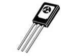
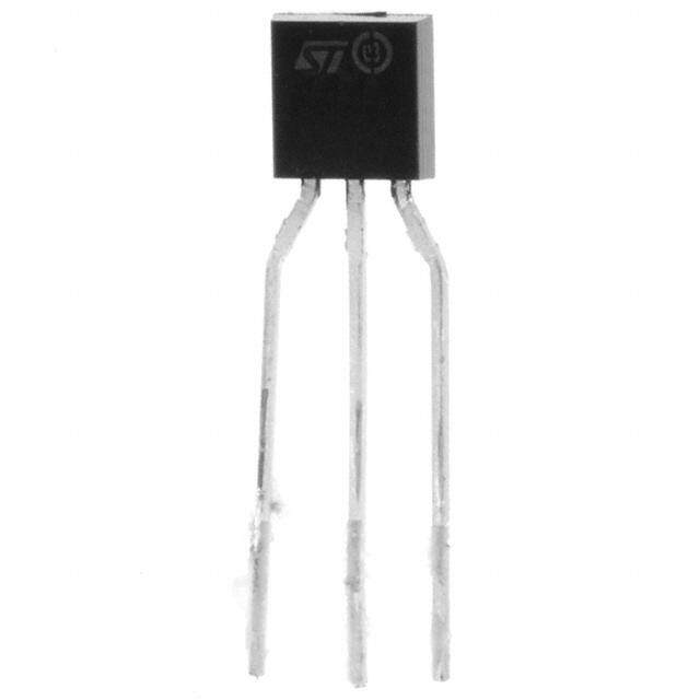
| 描述 | TRANS NPN 80V 3A BIPO TO-225两极晶体管 - BJT 3A 80V 30W NPN |
| 产品分类 | 晶体管(BJT) - 单路分离式半导体 |
| 品牌 | ON Semiconductor |
| 产品手册 | |
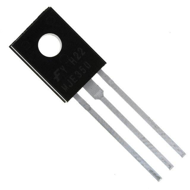
| 产品图片 |
|
| rohs | 符合RoHS无铅 / 符合限制有害物质指令(RoHS)规范要求 |
| 产品系列 | 晶体管,两极晶体管 - BJT,ON Semiconductor BD179G- |
| 数据手册 | |
| 产品型号 | BD179G |
| 不同 Ib、Ic时的 Vce饱和值(最大值) | 800mV @ 100mA,1A |
| 不同 Ic、Vce 时的DC电流增益(hFE)(最小值) | 63 @ 150mA,2V |
| 产品种类 | 两极晶体管 - BJT |
| 供应商器件封装 | TO225AA |
| 其它名称 | BD179G-ND |
| 功率-最大值 | 30W |
| 包装 | 散装 |
| 发射极-基极电压VEBO | 5 V |
| 商标 | ON Semiconductor |
| 增益带宽产品fT | 3 MHz |
| 安装类型 | 通孔 |
| 安装风格 | Through Hole |
| 封装 | Bulk |
| 封装/外壳 | TO-225AA,TO-126-3 |
| 封装/箱体 | TO-225-3 |
| 工厂包装数量 | 500 |
| 晶体管极性 | NPN |
| 晶体管类型 | NPN |
| 最大功率耗散 | 30 W |
| 最大工作温度 | + 150 C |
| 最大直流电集电极电流 | 3 A |
| 最小工作温度 | - 65 C |
| 标准包装 | 500 |
| 电压-集射极击穿(最大值) | 80V |
| 电流-集电极(Ic)(最大值) | 3A |
| 电流-集电极截止(最大值) | - |
| 直流集电极/BaseGainhfeMin | 63 |
| 系列 | BD179 |
| 配置 | Single |
| 集电极—发射极最大电压VCEO | 80 V |
| 集电极—基极电压VCBO | 80 V |
| 集电极—射极饱和电压 | 0.8 V |
| 集电极连续电流 | 3 A |
| 频率-跃迁 | 3MHz |


- 商务部:美国ITC正式对集成电路等产品启动337调查
- 曝三星4nm工艺存在良率问题 高通将骁龙8 Gen1或转产台积电
- 太阳诱电将投资9.5亿元在常州建新厂生产MLCC 预计2023年完工
- 英特尔发布欧洲新工厂建设计划 深化IDM 2.0 战略
- 台积电先进制程称霸业界 有大客户加持明年业绩稳了
- 达到5530亿美元!SIA预计今年全球半导体销售额将创下新高
- 英特尔拟将自动驾驶子公司Mobileye上市 估值或超500亿美元
- 三星加码芯片和SET,合并消费电子和移动部门,撤换高东真等 CEO
- 三星电子宣布重大人事变动 还合并消费电子和移动部门
- 海关总署:前11个月进口集成电路产品价值2.52万亿元 增长14.8%


PDF Datasheet 数据手册内容提取
BD179G Plastic Medium-Power Silicon NPN Transistor This device is designed for use in 5.0 to 10 Watt audio amplifiers and drivers utilizing complementary or quasi complementary circuits. Features http://onsemi.com • High DC Current Gain • BD179 is complementary with BD180 3.0 AMPERES • These Devices are Pb−Free and are RoHS Compliant* POWER TRANSISTORS NPN SILICON MAXIMUM RATINGS 80 VOLTS, 30 WATTS Rating Symbol Value Unit Collector−Emitter Voltage VCEO 80 Vdc COLLECTOR Collector−Base Voltage VCBO 80 Vdc 2 Emitter−Base Voltage VEBO 5.0 Vdc Collector Current IC 3.0 Adc 3 Base Current IB 1.0 Adc BASE To@tal TPCo w=e 2r5 D(cid:2)iCssipation PD 30 W 1 Derate above 25(cid:2)C 240 mW/(cid:2)C EMITTER Operating and Storage Junction TJ, Tstg –65 to +150 (cid:2)C Temperature Range Stresses exceeding Maximum Ratings may damage the device. Maximum Ratings are stress ratings only. Functional operation above the Recommended Operating Conditions is not implied. Extended exposure to stresses above the TO−225 Recommended Operating Conditions may affect device reliability. CASE 77 STYLE 1 THERMAL CHARACTERISTICS Characteristic Symbol Max Unit 3 2 1 Thermal Resistance, Junction−to−Case R(cid:2)JC 4.16 (cid:2)C/W MARKING DIAGRAM YWW BD179G Y = Year WW = Work Week BD179 = Device Code G = Pb−Free Package ORDERING INFORMATION Device Package Shipping BD179G TO−225 500 Units/Box *For additional information on our Pb−Free strategy and soldering details, please (Pb−Free) download the ON Semiconductor Soldering and Mounting Techniques Reference Manual, SOLDERRM/D. © Semiconductor Components Industries, LLC, 2013 1 Publication Order Number: Noember, 2013 − Rev. 15 BD179/D
BD179G ELECTRICAL CHARACTERISTICS (TC = 25(cid:2)C unless otherwise noted) Characteristic Symbol Min Max Unit Collector−Emitter Sustaining Voltage (Note 1) V(BR)CEO Vdc (IC = 0.1 Adc, IB = 0) 80 − Collector Cutoff Current ICBO mAdc (VCB = 80 Vdc, IE = 0) − 0.1 Emitter Cutoff Current IEBO mAdc (VBE = 5.0 Vdc, IC = 0) − 1.0 DC Current Gain hFE − (IC = 0.15 A, VCE = 2.0 V) 63 160 (IC = 1.0 A, VCE = 2.0 V) 15 − Collector−Emitter Saturation Voltage (Note 1) VCE(sat) Vdc (IC = 1.0 Adc, IB = 0.1 Adc) − 0.8 Base−Emitter On Voltage (Note 1) VBE(on) Vdc (IC = 1.0 Adc, VCE = 2.0 Vdc) − 1.3 Current−Gain − Bandwidth Product fT MHz (IC = 250 mAdc, VCE = 10 Vdc, f = 1.0 MHz) 3.0 − 1. Pulse Test: Pulse Width ≤ 300 As, Duty Cycle ≤ 2.0%. 10 The Safe Operating Area Curves indicate IC − VCE limits 100 (cid:3)s P)7.0 below which the device will not enter secondary breakdown. M NT (A53..00 1.0 ms Capopllleiccatobrle l oSaadfe l iAneres af otor sapveociidf icca cuisricnugi tas cmautasstt rfoalplh wici tfhaiinlu trhee. RE2.0 5.0 ms To insure operation below the maximum T , R J CU dc power−temperature derating must be observed for both OR 1.0 TJ = 150°C steady state and pulse power conditions. T0.7 C LE0.5 SECONDARY BREAKDOWN LIMITATION L O THERMAL LIMITATION C0.3 I, C0.2 (SBIGASNEIF-IECMANITTT EARBO DVISES IICP A=T 2I.O0N A MISP) PULSE DUTY CYCLE < 10% 0.1 1.0 2.0 3.0 5.0 7.0 10 20 30 50 70 100 VCE, COLLECTOR-EMITTER VOLTAGE (VOLTS) Figure 1. Active Region Safe Operating Area http://onsemi.com 2
BD179G S) 1.0 T L O V GE ( 0.8 TA IC = 0.1 A 0.25 A 0.5 A 1.0 A L O V R 0.6 E MITT TJ = 25°C -E 0.4 R O T C E L 0.2 L O C , E C V 0 0.2 0.3 0.5 1.0 2.0 3.0 5.0 10 20 30 50 100 200 IB, BASE CURRENT (mA) Figure 2. Collector Saturation Region 1000 1.5 LIZED) 750000 VCE = 2.0 V TJ = 25°C A 1.2 M R 300 O URRENT GAIN (N 1275000000 TTJJ == ++ 12550°C°C OLTAGE (VOLTS) 00..96 VBE(sat) @ VICB/EIB @ = V10CE = 2.0 V C V DC 30 TJ = + 55°C 0.3 , E 20 hF VCE(sat) @ IC/IB = 10 10 0 2.03.0 5.0 10 20 30 50 100 200300 500 10002000 2.03.0 5.0 10 20 30 50 100 200300 500 10002000 IC, COLLECTOR CURRENT (mA) IC, COLLECTOR CURRENT (mA) Figure 3. Current Gain Figure 4. “On” Voltages 1.0 T N 0.7 D = 0.5 E SI 0.5 N A E TRNCE 0.3 D = 0.2 VA 0.2 ED EFFECTIMAL RESIST00.0.17 DDD === 000...00151 SINGLE PULSE (cid:2)(cid:2)(cid:2)JJJCCC( ==t) 43=.. 15r(6°t)C° C(cid:2)/WJ/WC T MYPAX P(pk) LIZER0.05 D CURVES APPLY FOR POWER MATH PULSE TRAIN SHOWN t1 NOR 00..0032 READ TIME AT t1 t2 r(t), TJ(pk) - TC = P(pk) (cid:2)JC(t) DUTY CYCLE, D = t1/t2 0.01 0.01 0.020.03 0.05 0.1 0.2 0.3 0.5 1.0 2.0 3.0 5.0 10 20 30 50 100 200 300 500 1000 t, TIME or PULSE WIDTH (ms) Figure 5. Thermal Response http://onsemi.com 3
BD179G PACKAGE DIMENSIONS TO−225 CASE 77−09 ISSUE AB E A1 NOTES: 1.DIMENSIONING AND TOLERANCING PER Q A ASME Y14.5M, 1994. 2.CONTROLLING DIMENSION: MILLIMETERS. 3.NUMBER AND SHAPE OF LUGS OPTIONAL. MILLIMETERS DIM MIN MAX A 2.40 3.00 D A1 1.00 1.50 P b 0.60 0.90 b2 0.51 0.88 c 0.39 0.63 1 2 3 D 10.60 11.10 E 7.40 7.80 e 2.04 2.54 L 14.50 16.63 L1 1.27 2.54 L1 P 2.90 3.30 Q 3.80 4.20 L STYLE 1: PIN 1. EMITTER 2. COLLECTOR 3. BASE 2X b2 2X e b c ON Semiconductor and are registered trademarks of Semiconductor Components Industries, LLC (SCILLC). SCILLC owns the rights to a number of patents, trademarks, copyrights, trade secrets, and other intellectual property. A listing of SCILLC’s product/patent coverage may be accessed at www.onsemi.com/site/pdf/Patent−Marking.pdf. SCILLC reserves the right to make changes without further notice to any products herein. SCILLC makes no warranty, representation or guarantee regarding the suitability of its products for any particular purpose, nor does SCILLC assume any liability arising out of the application or use of any product or circuit, and specifically disclaims any and all liability, including without limitation special, consequential or incidental damages. “Typical” parameters which may be provided in SCILLC data sheets and/or specifications can and do vary in different applications and actual performance may vary over time. All operating parameters, including “Typicals” must be validated for each customer application by customer’s technical experts. SCILLC does not convey any license under its patent rights nor the rights of others. SCILLC products are not designed, intended, or authorized for use as components in systems intended for surgical implant into the body, or other applications intended to support or sustain life, or for any other application in which the failure of the SCILLC product could create a situation where personal injury or death may occur. Should Buyer purchase or use SCILLC products for any such unintended or unauthorized application, Buyer shall indemnify and hold SCILLC and its officers, employees, subsidiaries, affiliates, and distributors harmless against all claims, costs, damages, and expenses, and reasonable attorney fees arising out of, directly or indirectly, any claim of personal injury or death associated with such unintended or unauthorized use, even if such claim alleges that SCILLC was negligent regarding the design or manufacture of the part. SCILLC is an Equal Opportunity/Affirmative Action Employer. This literature is subject to all applicable copyright laws and is not for resale in any manner. PUBLICATION ORDERING INFORMATION LITERATURE FULFILLMENT: N. American Technical Support: 800−282−9855 Toll Free ON Semiconductor Website: www.onsemi.com Literature Distribution Center for ON Semiconductor USA/Canada P.O. Box 5163, Denver, Colorado 80217 USA Europe, Middle East and Africa Technical Support: Order Literature: http://www.onsemi.com/orderlit Phone: 303−675−2175 or 800−344−3860 Toll Free USA/Canada Phone: 421 33 790 2910 Fax: 303−675−2176 or 800−344−3867 Toll Free USA/Canada Japan Customer Focus Center For additional information, please contact your local Email: orderlit@onsemi.com Phone: 81−3−5817−1050 Sales Representative http://onsemi.com BD179/D 4
Mouser Electronics Authorized Distributor Click to View Pricing, Inventory, Delivery & Lifecycle Information: O N Semiconductor: BD179G