ICGOO在线商城 > 集成电路(IC) > PMIC - 稳压器 - 线性 > AS1363-BSTT-15

 Datasheet下载
- 型号: AS1363-BSTT-15
- 制造商: AUSTRIAMICROSYSTEMS
- 库位|库存: xxxx|xxxx
- 要求:
| 数量阶梯 | 香港交货 | 国内含税 |
| +xxxx | $xxxx | ¥xxxx |
查看当月历史价格
查看今年历史价格
AS1363-BSTT-15产品简介:
ICGOO电子元器件商城为您提供AS1363-BSTT-15由AUSTRIAMICROSYSTEMS设计生产,在icgoo商城现货销售,并且可以通过原厂、代理商等渠道进行代购。 AS1363-BSTT-15价格参考。AUSTRIAMICROSYSTEMSAS1363-BSTT-15封装/规格:PMIC - 稳压器 - 线性, Linear Voltage Regulator IC Positive Fixed 1 Output 1.5V 500mA SOT-23-6。您可以下载AS1363-BSTT-15参考资料、Datasheet数据手册功能说明书,资料中有AS1363-BSTT-15 详细功能的应用电路图电压和使用方法及教程。
AS1363-BSTT-15 是奥地利微电子公司(ams)推出的一款线性稳压器,属于PMIC(电源管理集成电路)类别。该器件为高精度、低噪声的线性稳压器,适用于对电源稳定性与噪声抑制要求较高的应用场景。

该型号主要应用于以下领域:

1. 便携式医疗设备:如血糖仪、血压计等,因其具备低噪声和高稳定性特点,可保障测量精度和信号完整性。

2. 工业传感器与仪表:用于提供稳定电压供电,确保传感器数据采集的准确性。

3. 射频(RF)模块与通信设备:适合为敏感的射频电路或低噪声放大器(LNA)供电,降低电源噪声对信号质量的影响。

4. 音频设备:如高端耳机放大器、录音设备,利用其低纹波和低噪声特性提升音质表现。

5. 电池供电系统:由于其较低静态电流设计,有助于延长电池续航时间,适用于各类手持式电子设备。

总之,AS1363-BSTT-15 适用于需要高精度、低噪声电源调节的小功率应用场合,尤其适合对电源稳定性有较高要求的精密电子系统。
| 参数 | 数值 |
| 产品目录 | 集成电路 (IC) |
| 描述 | IC REG LDO 1.5V 0.5A SOT23-6 |
| 产品分类 | |
| 品牌 | ams |
| 数据手册 | http://www.ams.com/eng/content/download/12507/219217 |
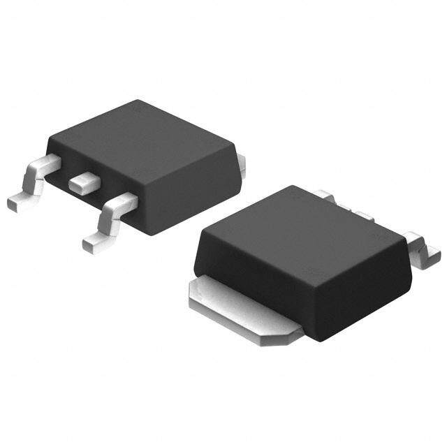
| 产品图片 |
|
| 产品型号 | AS1363-BSTT-15 |
| rohs | 无铅 / 符合限制有害物质指令(RoHS)规范要求 |
| 产品系列 | - |
| 供应商器件封装 | SOT-23-6 |
| 其它名称 | AS1363-BSTT-15CT |
| 包装 | 剪切带 (CT) |
| 安装类型 | 表面贴装 |
| 封装/外壳 | SOT-23-6 |
| 工作温度 | -40°C ~ 85°C |
| 标准包装 | 1 |
| 电压-跌落(典型值) | - |
| 电压-输入 | 2 V ~ 5.5 V |
| 电压-输出 | 1.5V |
| 电流-输出 | 500mA |
| 电流-限制(最小值) | - |
| 稳压器拓扑 | 正,固定式 |
| 稳压器数 | 1 |


PDF Datasheet 数据手册内容提取
Datasheet AS1363 500mA, Low-Dropout Linear Voltage Regulator 1 General Description 2 Key Features The AS1363 is a low-dropout linear regulator that oper- ! Guaranteed Output Current: 500mA ates from a +2.0V to +5.5V supply and delivers a guar- ! Low Dropout: 150mV @ 500mA anteed 500mA load current with low 150mV dropout. The device is available in two versions (see Table 1). ! 2.0V to 5.5V Input Voltage One version has a high-accuracy output with a preset ! Fixed Output Voltage: 1.2V to 5.0V voltage (1.2, 1.5, 1.8, 3.0, 3.3, or 4.5V). This voltage is internally trimmed and also offers a Bypass pin. With a ! User-Adjustable Output Voltage: 1.2V to 5.3V capacitor connected to this Bypass pin, the PSRR and the Noise performance is improved. ! Power OK Output At the other version the output voltage is user-adjustable ! Low Quiescent Current: 40µA (1.2V to 5.3V) and offers an SET pin for setting the out- put voltage. ! Low Shutdown Current: 30nA Table 1. Standard Products ! Thermal Overload Protection Model Output Type BYP SET ! Output Current Limit AS1363-AD Adjustable No Yes ! 6-pin SOT23 Package AS1363-_ _ Fixed Yes No 3 Applications A low supply current (65µA typ.) at maximum load is making the device ideal for portable battery-operated equipment. The device is ideal for laptops, PDAs, portable audio devices, mobile phones, cordless phones, and any other Other features are included such as an active-low open- battery-operated portable device. drain reset output that indicates when the output is out of regulation, a low-current (30nA typ.) shutdown mode, an integrated short-circuit and a thermal shutdown pro- tection. The AS1363 is available in a 6-pin SOT23 package. Figure 1. AS1363 - Typical Application Circuit VIN 1 6 VOUT 2.0V to 5.5V IN OUT 1.2V to 5.3V CIN COUT 1µF 2.2µF R1 AS1363-AD On 3 5 Off EN SET R2 2 4 To Controller POK GND RPOK 100kΩ VOUT Logic Supply Voltage www.austriamicrosystems.com/LDOs/AS1363 Revision 1.05 1 - 14
AS1363 Datasheet - Pinout 4 Pinout Pin Assignments Figure 2. Pin Assignments (Top View) IN 1 6 OUT POK 2 AS1363 5 SET/BYP EN 3 4 GND Pin Descriptions Table 2. Pin Descriptions Pin Number Pin Name Description +2.0V to +5.5V Supply Voltage. Bypass this pin with a 1µF capacitor to GND (see 1 IN Capacitor Selection and Regulator Stability on page 11). Open-Drain POK Output. POK remains low while VOUT is below the POK 2 POK threshold. Connect a 100kΩ pull-up resistor from this pin to OUT to obtain an output voltage (see Figure 1 on page 1). Active-High Enable Input. A logic low reduces supply current below 30nA. In 3 EN shutdown mode, the POK output is low, and OUT is high impedance. Connect this pin to IN for normal operation. 4 GND Ground Voltage-Setting Input. Connect to GND for preset output or Connect to a resistive SET voltage-divider between OUT and GND to set the output voltage between 1.2V and 5 5.3V (see Figure 1 on page 1). Bypass Pin. Connect a 10nF capacitor from this pin to VOUT to improve PSRR and BYP noise performance (see Figure 16 on page 9). Output. Sources up to 500mA. Bypass this pin with a 2.2µF low-ESR capacitor to 6 OUT GND (see Figure 1 on page 1). Note: For output voltages below 2V a 4.7µF capacitor should be used. www.austriamicrosystems.com/LDOs/AS1363 Revision 1.05 2 - 14
AS1363 Datasheet - Absolute Maximum Ratings 5 Absolute Maximum Ratings Stresses beyond those listed in Table 3 may cause permanent damage to the device. These are stress ratings only, and functional operation of the device at these or any other conditions beyond those indicated in Electrical Character- istics on page 4 is not implied. Exposure to absolute maximum rating conditions for extended periods may affect device reliability. Table 3. Absolute Maximum Ratings Parameter Min Max Units Comments IN, POK, EN, SET/BYP to GND -0.3 +6 V OUT to GND -0.3 VIN +0.3 V Output Short-Circuit Duration 1 min Continuous Power Dissipation 800 mW TAMB = +70ºC; derate 10mW/ºC above +70ºC Operating Temperature Range -40 +85 ºC Storage Temperature Range -65 +150 ºC Junction Temperature +150 ºC The reflow peak soldering temperature (body temperature) specified is in accordance with IPC/JEDEC J-STD-020D “Moisture/Reflow Package Body Temperature +260 ºC Sensitivity Classification for Non-Hermetic Solid State Surface Mount Devices”. The lead finish for Pb-free leaded packages is matte tin (100% Sn). www.austriamicrosystems.com/LDOs/AS1363 Revision 1.05 3 - 14
AS1363 Datasheet - Electrical Characteristics 6 Electrical Characteristics VIN = VOUT(NOM) + 500mV or VIN = +2.0V (whichever is greater), CIN = 1µF, COUT = 2.2µF, EN = IN, TAMB = -40 to +85ºC (unless otherwise specified). Typical values are at TAMB = +25ºC. Table 4. Electrical Characteristics Symbol Parameter Condition Min Typ Max Unit VIN Input Voltage 2.0 5.5 V VPOR Power On reset Falling, 100mV hysteresis 1.78 1.87 1.96 V IOUT = 100mA, TAMB = +25ºC, -0.75 +0.75 Output Voltage Accuracy IOUT = 100mA -1.5 +1.5 % (Preset Mode) IOUT = 1 to 500mA, VIN > (VOUT + 0.5V)1 -2 +2 Adjustable Output Voltage VOUT 1.2 5.3 V Range VSET/BYP SET/BYP Voltage Threshold VIN = 2.5V, IOUT = 100mA, 1.17 1.20 1.23 V (Adjustable Mode) VOUT set to 2.0V Guaranteed Output Current IOUT 500 mA (RMS) ILIMIT Short-Circuit Current Limit VOUT = 0V 0.55 0.8 1.2 A In-Regulation Current Limit VOUT > 96% of nominal value 0.8 A SET/BYP Threshold 50 100 150 mV ISET SET/BYP Input Bias Current VSET/BYP = 1.2V -100 +100 nA IOUT = 100µA 40 150 IQ Quiescent Current µA IOUT = 500mA 65 200 VVOINU T- Dropout Voltage 2 IOUT = 500mA VOUT = 2.5V 150 320 mV ΔVLNR Line Regulation VIN from (VOUT + 100mV) to 5.5V, -0.125 +0.125 %/V ILOAD = 5mA ΔVLDR Load Regulation IOUT = 1 to 500mA -0.001 +0.001 %/mA f = 1kHz, IOUT = 10mA, adjustable Output 65 f = 10kHz, IOUT = 10mA, adjustable 70 PSRR Ripple Rejection Output dB f = 100kHz, IOUT = 10mA, adjustable 60 Output 10Hz to 100kHz, IOUT = 10mA, adjustable 80 Output Output Voltage Noise µVRMS 100Hz to 100kHz, IOUT = 10mA, 65 adjustable Output Shutdown EN = GND, VIN = 5.5V, TAMB = 25°C 0.03 0.5 IOFF Shutdown Supply Current µA EN = GND, VIN = 5.5V 15 VIH 2.0V < VIN < 5.5V 1.6 V EN Input Threshold VIL 2.0V < VIN < 5.5V 0.6 V EN = IN or GND, TAMB = +25ºC 1 IEN EN Input Bias Current nA TAMB = +85ºC 5 www.austriamicrosystems.com/LDOs/AS1363 Revision 1.05 4 - 14
AS1363 Datasheet - Electrical Characteristics Table 4. Electrical Characteristics (Continued) Symbol Parameter Condition Min Typ Max Unit POK Output VOL POK Output Low Voltage POK sinking 1mA 0.05 0.25 V Operating Voltage Range for POK sinking 100µA 1.1 5.5 V Valid POK Signal POK Output High leakage POK = 5.5V, TAMB = +25ºC 1 nA Current TAMB = +85ºC 5 POK Threshold Rising edge (referenced to VOUT(NOM)) 90 94 98 % Thermal Protection Thermal Shutdown TSHDNN 170 ºC Temperature ΔTSHDNN Thermal Shutdown Hysteresis 20 ºC 1.Guaranteed by production test of load regulation and line regulation. 2.Dropout voltage is defined as VIN - VOUT, when VOUT is 100mV below the value of VOUT measured for VIN = (VOUT(NOM) + 500mV). Since the minimum input voltage is 2.0V, this specification is only valid when VOUT(NOM) > 2.0V. Note: All limits are guaranteed. The parameters with min and max values are guaranteed with production tests or SQC (Statistical Quality Control) methods. www.austriamicrosystems.com/LDOs/AS1363 Revision 1.05 5 - 14
AS1363 Datasheet - Typical Operating Characteristics 7 Typical Operating Characteristics VIN = VOUT(NOM) + 0.5V, CIN = 1µF, COUT = 2.2µF, TAMB = 25°C (unless otherwise specified). Figure 3. VDROP vs. IOUT; Figure 4. VOUT vs. IOUT; VOUT(NOM) = 2.5V 160 2.503 140 mV)120 V)2.502 e (100 e ( g g a a olt 80 olt2.501 V V out 60 put p ut o O Dr 40 2.5 20 0 2.499 0 100 200 300 400 500 0 100 200 300 400 500 Load Current (mA) Output Current (mA) Figure 5. VOUT vs. Temperature; VOUT(NOM) = 2.5V Figure 6. VOUT vs. VIN; VOUT(NOM) = 2.5V 2.505 3 2.504 Iout = 0mA 2.5 Iout = 500mA 2.503 V) V) e (2.502 e ( 2 g g olta2.501 olta1.5 V V ut 2.5 ut p p ut2.499 ut 1 O O 2.498 0.5 2.497 2.496 0 -45 -30 -15 0 15 30 45 60 75 90 0 0.5 1 1.5 2 2.5 3 Temperature (°C) Input Voltage (V) Figure 7. Quiescent Current vs. VIN; no load Figure 8. Quiescent Current vs. IOUT; VIN = 3.0V; 120 100 100 A) A) 80 µ µ nt ( 80 nt ( e e 60 rr rr u u C 60 C nt nt e e 40 c c s 40 s e e ui ui Q Q 20 20 0 0 0 1 2 3 4 5 6 0 100 200 300 400 500 Input Voltage (V) Output Current (mA) www.austriamicrosystems.com/LDOs/AS1363 Revision 1.05 6 - 14
AS1363 Datasheet - Typical Operating Characteristics Figure 9. Quiescent Current vs. Temperature; Figure 10. PSRR vs. Frequency; IOUT = 10mA, VIN = 3.0V CIN = 68nF, 100 -50 A) 80 µ -60 ent ( 60 B) Curr R (d-70 cent 40 PSR s e ui -80 Q 20 no load Iout = 100mA 0 -90 -45 -30 -15 0 15 30 45 60 75 90 10 100 1000 10000 100000 Temperature (°C) Frequency (Hz) Figure 11. Line Transient Response; Figure 12. Load Transient Response; VIN = 3.0V to 3.5V, IOUT = 100mA VIN = 3.0V, IOUT = 50mA to 250mA v T Di Div VOU mV/ VIN 0mV/ 50 0 2 V VOUT 0mV/DIV IOUT 100mA/DI 2 1ms/Div 5µs/Div Figure 13. Startup; VIN = 3.0V, IOUT = 100mA Figure 14. Startup; VIN = 3.0V, IOUT = 100mA v v Di Di EN V/ EN V/ 1 1 V V DI DI OUT 1V/ OUT 1V/ V V 1ms/Div 20µs/Div www.austriamicrosystems.com/LDOs/AS1363 Revision 1.05 7 - 14
AS1363 Datasheet - Detailed Description 8 Detailed Description The AS1363 is a low-dropout, low-quiescent-current linear regulator specifically designed for battery-powered devices. The regulator supplies loads of up to 500mA and can deliver a factory-preset output voltage or user-adjustable output voltage. The device features a 1.2V reference, error amplifier, P-channel pass transistor, and internal feedback voltage-divider (see Figure 15). Additional blocks include an output current limiter, thermal sensor, and shutdown logic. Figure 15. Block Diagram VIN 2.0V to 5.5V 1 IN CIN Thermal 1µF Sensor MOSFET Driver w/ILIM VOUT 6 1.2V to 5.3V On 3 Shutdown OUT Off Logic COUT EN 2.2µF 1.2V 5kΩ + Reference Error – R1 VOUT Logic Amplifier Supply Voltage RPOK 100kΩ 2 To Controller 5 POK + SET + – – R2 + + 93%VREF – 100mV – 4 AS1363-AD GND The 1.2V reference is connected to the error amplifier, which compares this reference with the feedback voltage and amplifies the difference. If the feedback voltage is lower than the reference voltage, the pass-transistor gate is pulled lower, allowing more current to pass to the output and increases the output voltage. If the feedback voltage is too high, the pass transistor gate is pulled up, allowing less current to pass to the output. The output voltage is delivered back through either an internal resistive divider connected to OUT or an external resis- tor network connected to SET (see Figure 15). The comparator examines VSET/BYP and selects the feedback path. If VSET/BYP is less than 50mV, the internal feedback path is used and the output is regulated to the factory-preset voltage (see Ordering Information on page 13). Internal P-Channel Pass Transistor The AS1363 features a P-channel MOSFET pass transistor and consumes only a maximum of 200µA of quiescent current under heavy loads as well as in dropout. Shutdown If pin EN is connected to GND the AS1363 is disabled. In shutdown mode all internal circuits are turned off, reducing supply current to 30nA (typ.). For normal operation pin EN must be connected to IN. During shutdown, POK is low. www.austriamicrosystems.com/LDOs/AS1363 Revision 1.05 8 - 14
AS1363 Datasheet - Detailed Description Output Voltage Selection The AS1363 is available in two versions (see Ordering Information on page 13). One version can only operate at one fixed output voltage and the other version can operate with a preset output voltage or with user-adjustable output volt- ages (1.2V to 5.3V). ! For the fixed output voltage version connect a capacitor CBYP from pin BYP to VOUT to improve PSRR and Noise performance (see Figure 16). ! To use the factory preset output voltage of the user-adjustable output voltage version, connect pin SET to GND (see Figure 17). ! For configurations using an output voltage other than the factory preset, a voltage-divider from OUT to SET to GND is required, as shown in (see Figure 1 on page 1). A value for R2 in the 25kΩ to 100kΩ range should be suf- ficient. Calculate the value for R1 as: V R = R ×⎛--------O----U----T-----–1⎞ (EQ 1) 1 2 ⎝V ⎠ SETBYP Where: VOUT is in a range from 1.2V to 5.3V. VSET/BYP = 1.2V. Figure 16. Fixed Output Voltage VIN 1 6 VOUT 2.0V to 5.5V 1.2V to 5.0V IN OUT CIN COUT 1µF RPOK 2.2µF 100kΩ On 3 AS1363 2 To Controller Off EN POK CBYP 10nF 4 5 GND BYP Figure 17. Adjustable Output using preset Output Voltage VIN 1 6 VOUT 2.5V to 5.5V 2.5V IN OUT CIN COUT 1µF RPOK 2.2µF 100kΩ On 3 AS1363-AD 2 To Controller Off EN POK 4 5 GND SET www.austriamicrosystems.com/LDOs/AS1363 Revision 1.05 9 - 14
AS1363 Datasheet - Detailed Description Power-OK The AS1363 features a power-ok indicator that asserts when the output voltage falls out of regulation. The open-drain POK output goes low when output voltage at OUT falls 6% below its nominal value. A 100kΩ pull-up resistor from POK to a (typically OUT) provides a logic control signal. POK can be used as a power-on-reset (POR) signal to a microcontroller or can drive an external LED to indicate a power failure condition. Note: POK is low during shutdown. Current Limit The AS1363 features current limiting circuitry that monitors the pass transistor, limiting short-circuit output current to 0.8A (typ). The circuitry of the AS1363 allows that the output can be shorted to ground for an indefinite period of time without damaging the device. Thermal Overload Protection Integrated thermal overload protection limits the total power dissipation in the AS1363. When the junction temperature (TJ) exceeds +170ºC typically, the pass transistor is turned off. Normal operation is continued when TJ drops approxi- mately 20ºC. Note: Regardless of the hysteresis, continuous short-circuit condition will result in a pulsed output. Operating Region and Power Dissipation Maximum power dissipation depends on the thermal resistance of the IC package and circuit board, the temperature difference between the die junction and ambient air, and the rate of air flow. The power dissipated in the device is given as: PD = I ×(V –V ) (EQ 2) OUT IN OUT The AS1363 can deliver up to 0.5A RMS and operates with input voltages up to +5.5V, but not at the same time. High output currents can only be sustained when input/output differential voltages are low. The maximum allowed power dissipation is 800mW at TAMB = +70ºC or: T –T PDMAX = ----J--(--m----a---x--)-----------A----M----B-- (EQ 3) θ +θ JC JA Where: TJ(MAX) - TAMB is the temperature difference between the device die junction and the surrounding air. θJC is the thermal resistance of the junction to the case. θJA is the thermal resistance from the case through the PCB, copper traces, and other materials to the surrounding air. Note: For best heat transfer, the copper area should be equally shared between the IN, OUT, and GND pins. www.austriamicrosystems.com/LDOs/AS1363 Revision 1.05 10 - 14
AS1363 Datasheet - Application Information 9 Application Information Capacitor Selection and Regulator Stability Input and output capacitors are required for stable operation of the AS1363 over the full temperature range and with load currents up to 500mA. Connect CIN and COUT as close to the AS1363 as possible to minimize the impact of PC board trace inductance. For CIN, connect a 1µF capacitor between IN and ground. CIN lowers the source impedance of the input supply. Reduce noise and improve load-transient response, stability, and power supply rejection by using larger output capac- itors, such as 10µF. For COUT connect a 2.2µF low-ESR capacitor between OUT and ground. The output capacitor’s ESR affects stability and output noise. Use output capacitors with an ESR of 0.1Ω or less to ensure stability and optimum transient response. Surface-mount ceramic capacitors have very-low ESR and are commonly available in values up to 10µF. For output voltages less than 2V, use a 4.7µF low-ESR output capacitor for COUT. Noise, Power Supply Rejection Ratio, and Transient Response The AS1363 is designed to operate with low dropout voltages and low quiescent currents in battery-powered systems while still maintaining good noise response, transient response, and AC rejection. See Typical Operating Characteris- tics on page 6 for a plot of power-supply rejection ratio (PSRR) versus frequency. When operating from noisy sources, improved supply-noise rejection and transient response can be achieved by increasing the values of the input and out- put bypass capacitors and through passive filtering techniques. Dropout Voltage Because the AS1363 uses a P-channel MOSFET pass transistor, its dropout voltage is a function of drain-to-source on-resistance (RDS(ON)) multiplied by the load current: V = V –V = R ×I (EQ 4) DROPOUT IN OUT DS(ON) OUT Note: The AS1363 ground current remains below 200µA in dropout. www.austriamicrosystems.com/LDOs/AS1363 Revision 1.05 11 - 14
AS1363 Datasheet - Package Drawings and Markings 10 Package Drawings and Markings The device is available in an 6-pin SOT23 package. Figure 18. 6-pin SOT23 Package Symbol Min Nom Max A 0.90 1.45 A1 0.00 0.15 A2 0.90 1.30 b 0.30 0.50 Notes: C 0.09 0.20 1. Dimensions are in millimeters (mm). D 2.80 3.05 E 2.60 3.00 2. Foot length measured at intercept point between datum A and lead surface. E1 1.50 1.75 L 0.30 0.55 3. Package outline exclusive of mold flash and metal burr. E 0.95Ref 4. Package outline inclusive of solder plating. e1 1.90Ref 5. Complies with EIAJ SC74A. α 0º 8º www.austriamicrosystems.com/LDOs/AS1363 Revision 1.05 12 - 14
AS1363 Datasheet - Ordering Information 11 Ordering Information The device is available as the standard products shown in Table 5. Table 5. Ordering Information Ordering Code Marking Output SET/BYP Delivery Form Package adjustable AS1363-BSTT-AD ASQ9 SET Tape and Reel 6-pin SOT23 (preset to 2.5V) AS1363-BSTT-12* ASRY 1.2V BYP Tape and Reel 6-pin SOT23 AS1363-BSTT-15 ASRA 1.5V BYP Tape and Reel 6-pin SOT23 AS1363-BSTT-18 ASRB 1.8V BYP Tape and Reel 6-pin SOT23 AS1363-BSTT-30 ASRC 3.0V BYP Tape and Reel 6-pin SOT23 AS1363-BSTT-33 ASRD 3.3V BYP Tape and Reel 6-pin SOT23 AS1363-BSTT-45 ASRE 4.5V BYP Tape and Reel 6-pin SOT23 *Future product. Non-standard devices are available between 1.4V and 4.6V in 50mV steps and between 4.6V and 5.0V in 100mV steps. For more information and inquiries contact http://www.austriamicrosystems.com/contact Note: All products are RoHS compliant. Buy our products or get free samples online at ICdirect: http://www.austriamicrosystems.com/ICdirect Technical Support is found at http://www.austriamicrosystems.com/Technical-Support For further information and requests, please contact us mailto:sales@austriamicrosystems.com or find your local distributor at http://www.austriamicrosystems.com/distributor www.austriamicrosystems.com/LDOs/AS1363 Revision 1.05 13 - 14
AS1363 Datasheet Copyrights Copyright © 1997-2010, austriamicrosystems AG, Tobelbaderstrasse 30, 8141 Unterpremstaetten, Austria-Europe. Trademarks Registered ®. All rights reserved. The material herein may not be reproduced, adapted, merged, translated, stored, or used without the prior written consent of the copyright owner. All products and companies mentioned are trademarks or registered trademarks of their respective companies. Disclaimer Devices sold by austriamicrosystems AG are covered by the warranty and patent indemnification provisions appearing in its Term of Sale. austriamicrosystems AG makes no warranty, express, statutory, implied, or by description regarding the information set forth herein or regarding the freedom of the described devices from patent infringement. austriamicrosystems AG reserves the right to change specifications and prices at any time and without notice. Therefore, prior to designing this product into a system, it is necessary to check with austriamicrosystems AG for current information. This product is intended for use in normal commercial applications. Applications requiring extended temperature range, unusual environmental requirements, or high reliability applications, such as military, medical life-support or life-sustaining equipment are specifically not recommended without additional processing by austriamicrosystems AG for each application. For shipments of less than 100 parts the manufacturing flow might show deviations from the standard production flow, such as test flow or test location. The information furnished here by austriamicrosystems AG is believed to be correct and accurate. However, austriamicrosystemsAG shall not be liable to recipient or any third party for any damages, including but not limited to personal injury, property damage, loss of profits, loss of use, interruption of business or indirect, special, incidental or consequential damages, of any kind, in connection with or arising out of the furnishing, performance or use of the technical data herein. No obligation or liability to recipient or any third party shall arise or flow out of austriamicrosystemsAG rendering of technical or other services. Contact Information Headquarters austriamicrosystems AG Tobelbaderstrasse 30 A-8141 Unterpremstaetten, Austria Tel: +43 (0) 3136 500 0 Fax: +43 (0) 3136 525 01 For Sales Offices, Distributors and Representatives, please visit: http://www.austriamicrosystems.com/contact www.austriamicrosystems.com/LDOs/AS1363 Revision 1.05 14 - 14