ICGOO在线商城 > 集成电路(IC) > PMIC - 稳压器 - 线性 > TPS70158PWP

 Datasheet下载
- 型号: TPS70158PWP
- 制造商: Texas Instruments
- 库位|库存: xxxx|xxxx
- 要求:
| 数量阶梯 | 香港交货 | 国内含税 |
| +xxxx | $xxxx | ¥xxxx |
查看当月历史价格
查看今年历史价格
TPS70158PWP产品简介:
ICGOO电子元器件商城为您提供TPS70158PWP由Texas Instruments设计生产,在icgoo商城现货销售,并且可以通过原厂、代理商等渠道进行代购。 TPS70158PWP价格参考¥17.50-¥32.51。Texas InstrumentsTPS70158PWP封装/规格:PMIC - 稳压器 - 线性, Linear Voltage Regulator IC Positive Fixed 2 Output 3.3V, 2.5V 500mA, 250mA 20-HTSSOP。您可以下载TPS70158PWP参考资料、Datasheet数据手册功能说明书,资料中有TPS70158PWP 详细功能的应用电路图电压和使用方法及教程。
TPS70158PWP 是 Texas Instruments(德州仪器)生产的一款线性稳压器(PMIC - Power Management IC),属于低功耗、低压差(LDO)稳压器系列。以下是其主要应用场景:

 1. 便携式电子设备
   - TPS70158PWP 的低静态电流(典型值为 25 µA)和小封装(WSON-8 封装)使其非常适合用于电池供电的便携式设备,例如:
     - 移动电话
     - 智能手表
     - 可穿戴设备
     - 便携式医疗设备(如脉搏血氧仪、血糖仪等)
   - 在这些应用中,低功耗特性可以显著延长电池寿命。

 2. 物联网 (IoT) 设备
   - 该芯片适用于需要稳定电源的 IoT 设备,例如:
     - 无线传感器节点
     - Zigbee 或 Bluetooth Low Energy (BLE) 模块
     - RFID 阅读器
   - 其高电源抑制比(PSRR)能够有效滤除噪声,确保敏感电路的正常运行。

 3. 嵌入式系统
   - 在嵌入式系统中,TPS70158PWP 可以为微控制器、存储器和其他低功耗外围设备提供稳定的电源电压。例如:
     - 工业控制模块
     - 数据采集系统
     - 家用自动化设备

 4. 音频和通信设备
   - 由于其低噪声性能(输出电压噪声低至 30 µVRMS),TPS70158PWP 适合为音频放大器和射频(RF)电路供电,以减少信号失真和干扰。具体应用包括:
     - 蓝牙耳机
     - 无线麦克风
     - GSM/CDMA 模块

 5. 消费类电子产品
   - 该稳压器可广泛应用于各种消费类电子产品中,例如:
     - 数码相机
     - MP3 播放器
     - 遥控器
   - 其紧凑的尺寸和简单的设计有助于降低整体解决方案的成本和复杂性。

 6. 汽车电子(非关键安全应用)
   - 在某些非关键安全的汽车电子应用中,TPS70158PWP 可以为以下设备供电:
     - 车载信息娱乐系统
     - 传感器接口
     - 后视摄像头模块

 总结
TPS70158PWP 的主要优势在于其低功耗、低噪声和高 PSRR 特性,这使得它成为电池供电设备、低功耗系统和对电源质量要求较高的应用的理想选择。通过提供稳定的电源输出,它可以确保系统的可靠性和性能。
| 参数 | 数值 |
| 产品目录 | 集成电路 (IC)半导体 |
| 描述 | IC REG LDO 3.3V/2.5V 20HTSSOP低压差稳压器 Dual 3.3/1.2V 500mA |
| 产品分类 | |
| 品牌 | Texas Instruments |
| 产品手册 | |
| 产品图片 |
|
| rohs | 符合RoHS无铅 / 符合限制有害物质指令(RoHS)规范要求 |
| 产品系列 | 电源管理 IC,低压差稳压器,Texas Instruments TPS70158PWP- |
| 数据手册 | |
| 产品型号 | TPS70158PWP |
| 产品目录页面 | |
| 产品种类 | 低压差稳压器 |
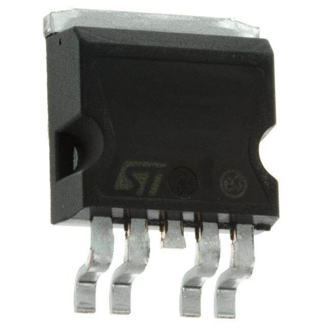
| 供应商器件封装 | 20-HTSSOP |
| 其它名称 | 296-2656-5 |
| 包装 | 管件 |
| 单位重量 | 81.800 mg |
| 参考电压 | 1.22 V |
| 商标 | Texas Instruments |
| 回动电压—最大值 | 275 mV |
| 安装类型 | 表面贴装 |
| 安装风格 | SMD/SMT |
| 封装 | Tube |
| 封装/外壳 | 20-TSSOP(0.173",4.40mm 宽)裸焊盘 |
| 封装/箱体 | HTSSOP-20 |
| 工作温度 | -40°C ~ 125°C |
| 工厂包装数量 | 70 |
| 最大功率耗散 | 4.115 W |
| 最大工作温度 | + 125 C |
| 最大输入电压 | 6 V |
| 最小工作温度 | - 40 C |
| 最小输入电压 | + 2.7 V |
| 标准包装 | 70 |
| 电压-跌落(典型值) | 0.17V @ 500mA,- |
| 电压-输入 | 2.7 V ~ 6 V |
| 电压-输出 | 3.3V,2.5V |
| 电压调节准确度 | 2 % |
| 电流-输出 | 500mA,250mA |
| 电流-限制(最小值) | - |
| 稳压器拓扑 | 正,固定式 |
| 稳压器数 | 2 |
| 系列 | TPS70158 |
| 线路调整率 | 0.01 % |
| 负载调节 | 1 mV |
| 输入偏压电流—最大 | 0.19 mA |
| 输出电压 | 3.3 V, 2.5 V |
| 输出电流 | 500 mA |
| 输出端数量 | 2 Output |
| 输出类型 | Fixed |
| 配用 | /product-detail/zh/TPS70151EVM-152/296-10986-ND/381844 |


PDF Datasheet 数据手册内容提取
TPS70145, TPS70148 TPS70151, TPS70158 TPS70102 www.ti.com SLVS222I–DECEMBER1999–REVISEDAUGUST2010 Dual-Output Low Dropout Voltage Regulators with Power-Up Sequencing for Split-Voltage DSP Systems CheckforSamples:TPS70145,TPS70148,TPS70151,TPS70158,TPS70102 FEATURES DESCRIPTION 1 • DualOutputVoltagesforSplit-Supply TPS701xx family devices are designed to provide a 23 Applications complete power management solution for the • SelectablePower-UpSequencingforDSP TMS320™ DSP family, processor power, ASIC, Applications FPGA, and digital applications where dual output voltage regulators are required. Easy programmability • OutputCurrentRangeof500mAonRegulator of the sequencing function makes the TPS701xx 1and250mAonRegulator2 family ideal for any TMS320 DSP applications with • FastTransientResponse power sequencing requirements. Differentiated • VoltageOptions:3.3V/2.5V,3.3V/1.8V, features, such as accuracy, fast transient response, SVS supervisory circuit, manual reset inputs, and an 3.3V/1.5V,3.3V/1.2V,andDualAdjustable enablefunction,provideacompletesystemsolution. Outputs • OpenDrainPower-OnResetwith120msDelay The TPS701xx family of voltage regulators offer very low dropout voltage and dual outputs with power-up • OpenDrainPowerGoodforRegulator1 sequence control, which is designed primarily for • UltraLow190mA(typ)QuiescentCurrent DSP applications. These devices have extremely low • 1mAInputCurrentDuringStandby noise output performance without using any added filter bypass capacitors and are designed to have a • LowNoise:65mV WithoutBypassCapacitor RMS fast transient response and be stable with 10mF low • QuickOutputCapacitorDischargeFeature ESRcapacitors. • TwoManualResetInputs These devices have fixed 3.3V/2.5V, 3.3V/1.8V, • 2%AccuracyOverLoadandTemperature 3.3V/1.5V, 3.3V/1.2V, and adjustable/adjustable • UndervoltageLockout(UVLO)Feature voltage options. Regulator 1 can support up to 500mA, and regulator 2 can support up to 250mA. • 20-PinPowerPAD™TSSOPPackage Separate voltage inputs allow the designer to • ThermalShutdownProtection configurethesourcepower. PWP PACKAGE (TOP VIEW) NC 1 20 NC VIN1 2 19 VOUT1 VIN1 3 18 VOUT1 MR1 4 17 V /FB1 SENSE1 MR2 5 16 PG1 EN 6 15 RESET SEQ 7 14 V /FB2 SENSE2 GND 8 13 V OUT2 V 9 12 V IN2 OUT2 V 10 11 NC IN2 1 Pleasebeawarethatanimportantnoticeconcerningavailability,standardwarranty,anduseincriticalapplicationsofTexas Instrumentssemiconductorproductsanddisclaimerstheretoappearsattheendofthisdatasheet. PowerPAD,TMS320aretrademarksofTexasInstruments. 2 Allothertrademarksarethepropertyoftheirrespectiveowners. 3 PRODUCTIONDATAinformationiscurrentasofpublicationdate. Copyright©1999–2010,TexasInstrumentsIncorporated Products conform to specifications per the terms of the Texas Instruments standard warranty. Production processing does not necessarilyincludetestingofallparameters.
TPS70145, TPS70148 TPS70151, TPS70158 TPS70102 SLVS222I–DECEMBER1999–REVISEDAUGUST2010 www.ti.com TPS70151 PWP DSP I/O 3.3 V 5 V VIN1 VOUT1 0.1 m F 10 m F VSENSE1 250 kW PG1 PG1 MR2 MR2 >2 V VIN2 <0.7 V 250 kW 0.1 m F RESET RESET >2 V EN MR1 MR1 >2 V EN <0.7 V <0.7 V VSENSE2 SEQ 1.8 V VOUT2 Core 10 m F Because the PMOS device behaves as a low-value resistor, the dropout voltage is very low (typically 170mV on regulator 1) and is directly proportional to the output current. Additionally, since the PMOS pass element is a voltage-driven device, the quiescent current is very low and independent of output loading (maximum of 230mA over the full range of output current). This LDO family also features a sleep mode; applying a high signal to EN (enable)shutsdownbothregulators,reducingtheinputcurrentto1mAatT =+25°C. J The device is enabled when the EN pin is connected to a low-level input voltage. The output voltages of the two regulatorsaresensedattheV andV pins,respectively. SENSE1 SENSE2 The input signal at the SEQ pin controls the power-up sequence of the two regulators. When the device is enabled and the SEQ terminal is pulled high or left open, V turns on first and V remains off until V OUT2 OUT1 OUT2 reaches approximately 83% of its regulated output voltage. At that time V is turned on. If V is pulled OUT1 OUT2 below 83% (for example, an overload condition), V is turned off. Pulling the SEQ terminal low reverses the OUT1 power-uporderandV isturnedonfirst.TheSEQpinisconnectedtoaninternalpull-upcurrentsource. OUT1 For each regulator, there is an internal discharge transistor to discharge the output capacitor when the regulator isturnedoff(disabled). The PG1 pin reports the voltage conditions at V , which can be used to implement an SVS for the circuitry OUT1 suppliedbyregulator1. The TPS701xx features a RESET (SVS, POR, or Power-On Reset). RESET output initiates a reset in DSP systems and related digital applications in the event of an undervoltage condition. RESET indicates the status of V and both manual reset pins (MR1 and MR2). When V reaches 95% of its regulated voltage and MR1 OUT2 OUT2 and MR2 are in the logic high state, RESET goes to a high impedance state after a 120ms delay. RESET goes to the logic low state when the V regulated output voltage is pulled below 95% (for example, an overload OUT2 condition)ofitsregulatedvoltage.TomonitorV ,thePG1outputpincanbeconnectedtoMR1orMR2. OUT1 The device has an undervoltage lockout (UVLO) circuit that prevents the internal regulators from turning on until V reaches2.5V. IN1 2 SubmitDocumentationFeedback Copyright©1999–2010,TexasInstrumentsIncorporated
TPS70145, TPS70148 TPS70151, TPS70158 TPS70102 www.ti.com SLVS222I–DECEMBER1999–REVISEDAUGUST2010 This integrated circuit can be damaged by ESD. Texas Instruments recommends that all integrated circuits be handled with appropriateprecautions.Failuretoobserveproperhandlingandinstallationprocedurescancausedamage. ESDdamagecanrangefromsubtleperformancedegradationtocompletedevicefailure.Precisionintegratedcircuitsmaybemore susceptibletodamagebecauseverysmallparametricchangescouldcausethedevicenottomeetitspublishedspecifications. ORDERINGINFORMATION(1) VOLTAGE(V)(2) PACKAGE- SPECIFIED LEAD TEMPERATURE ORDERING TRANSPORT PRODUCT V V (DESIGNATOR) RANGE(T ) NUMBER MEDIA,QUANTITY OUT1 OUT2 J TPS70102PWP Tube,70 TPS70102 Adjustable Adjustable HTSSOP-20(PWP) -40°Cto+125°C TPS70102PWPR TapeandReel,2000 TPS70145PWP Tube,70 TPS70145 3.3V 1.2V HTSSOP-20(PWP) -40°Cto+125°C TPS70145PWPR TapeandReel,2000 TPS70148PWP Tube,70 TPS70148 3.3V 1.5V HTSSOP-20(PWP) -40°Cto+125°C TPS70148PWPR TapeandReel,2000 TPS70151PWP Tube,70 TPS70151 3.3V 1.8V HTSSOP-20(PWP) -40°Cto+125°C TPS70151PWPR TapeandReel,2000 TPS70158PWP Tube,70 TPS70158 3.3V 2.5V HTSSOP-20(PWP) -40°Cto+125°C TPS70158PWPR TapeandReel,2000 (1) ForthemostcurrentpackageandorderinginformationseethePackageOptionAddendumlocatedattheendofthisdocument,orsee theTIwebsiteatwww.ti.com. (2) Forfixed1.20Voperation,tieFBtoOUT. ABSOLUTE MAXIMUM RATINGS(1) Overoperatingfree-airtemperaturerange(unlessotherwisenoted). TPS701xx UNIT Inputvoltagerange:V ,V (2) –0.3to+7 V IN1 IN2 VoltagerangeatEN –0.3to+7 V Outputvoltagerange(V ,V ) 5.5 V OUT1 SENSE1 Outputvoltagerange(V ,V ) 5.5 V OUT2 SENSE2 MaximumRESET,PG1voltage 7 V MaximumMR1,MR2,andSEQvoltage V V IN1 Peakoutputcurrent Internallylimited — Continuoustotalpowerdissipation SeeThermalInformationTable — Junctiontemperaturerange,T –40to+150 °C J Storagetemperaturerange,T –65to+150 °C stg ESDrating,HBM 2 kV (1) Stressesbeyondthoselistedunderabsolutemaximumratingsmaycausepermanentdamagetothedevice.Thesearestressratings only,andfunctionaloperationofthedeviceattheseoranyotherconditionsbeyondthoseindicatedunderrecommendedoperating conditionsisnotimplied.Exposuretoabsolute-maximum-ratedconditionsforextendedperiodsmayaffectdevicereliability. (2) Allvoltagesaretiedtonetworkground. Copyright©1999–2010,TexasInstrumentsIncorporated SubmitDocumentationFeedback 3
TPS70145, TPS70148 TPS70151, TPS70158 TPS70102 SLVS222I–DECEMBER1999–REVISEDAUGUST2010 www.ti.com THERMAL INFORMATION TPS701xx THERMALMETRIC(1)(2) UNITS PWP(20PINS) q Junction-to-ambientthermalresistance 74.1 JA q Junction-to-case(top)thermalresistance 43.1 JCtop q Junction-to-boardthermalresistance 19.7 JB °C/W y Junction-to-topcharacterizationparameter 2.9 JT y Junction-to-boardcharacterizationparameter 17.3 JB q Junction-to-case(bottom)thermalresistance 1.4 JCbot (1) Formoreinformationabouttraditionalandnewthermalmetrics,seetheICPackageThermalMetricsapplicationreport,SPRA953. (2) ForthermalestimatesofthisdevicebasedonPCBcopperarea,seetheTIPCBThermalCalculator. RECOMMENDED OPERATING CONDITIONS Overoperatingtemperaturerange(unlessotherwisenoted) MIN MAX UNIT Inputvoltage,V (1)(regulator1and2) 2.7 6 V I Outputcurrent,I (regulator1) 0 500 mA O Outputcurrent,I (regulator2) 0 250 mA O Outputvoltagerange(foradjustableoption) 1.22 5.5 V Operatingjunctiontemperature,T –40 +125 °C J (1) Tocalculatetheminimuminputvoltageformaximumoutputcurrent,usethefollowingequation:V =V +V . I(min) O(max) DO(maxload) ELECTRICAL CHARACTERISTICS Overrecommendedoperatingjunctiontemperaturerange(T =–40°Cto+125°C),V orV =V +1V,I =1mA, J IN1 IN2 OUT(nom) O EN=0V,C =33mF,(unlessotherwisenoted). O PARAMETER TESTCONDITIONS MIN TYP MAX UNIT Reference 2.7V<V <6V, I FBconnectedtoV 1.22 voltage T =+25°C O J 2.7V<V <6V, FBconnectedtoV 1.196 1.244 I O 1.2VOutput 2.7V<V <6V, T =+25°C 1.2 I J 2.7V<V <6V, 1.176 1.224 I 1.5VOutput 2.7V<V <6V, T =+25°C 1.5 I J Output VO voltage(1), 2.7V<VI<6V, 1.47 1.53 V (2) 1.8VOutput 2.7V<V <6V, T =+25°C 1.8 I J 2.7V<V <6V, 1.764 1.836 I 2.5VOutput 2.7V<V <6V, T =+25°C 2.5 I J 2.7V<V <6V, 2.45 2.55 I 3.3VOutput 2.7V<V <6V, T =+25°C 3.3 I J 2.7V<V <6V, 3.234 3.366 I Quiescentcurrent(GNDcurrent)for (2) TJ=+25°C 190 regulator1andregulator2,EN=0V(1) (2) 230 mA Ofourtrpeugtuvlaotlotarg1ealinnderreegguullaattoiorn2(∆(3V)O/VO) VVO++11VV<<VVI≤≤66VV, T(1J)=+25°C(1) 0.01% 0.1% V O I LoadregulationforV andV T =+25°C (2) 1 mV OUT1 OUT2 J (1) Minimuminputoperatingvoltageis2.7VorV +1V,whicheverisgreater.Maximuminputvoltage=6V,minimumoutput O(typ) current=1mA. (2) I =1mAto250mAforRegulator1and1mAto125mAforRegulator2. O (cid:5)VImax(cid:2)2.7V(cid:6) (3) IfV <1.8VthenV =6V,V =2.7V:LineReg.(mV)(cid:3)(%(cid:4)V)(cid:1)VO 100 (cid:1)1000 O Imax Imin (cid:6)VImax(cid:3)(cid:6)VO(cid:2)1V(cid:7)(cid:7) IfV >2.5VthenV =6V,V =V +1V:LineReg.(mV)(cid:4)(%(cid:5)V)(cid:1)VO 100 (cid:1)1000 O Imax Imin O 4 SubmitDocumentationFeedback Copyright©1999–2010,TexasInstrumentsIncorporated
TPS70145, TPS70148 TPS70151, TPS70158 TPS70102 www.ti.com SLVS222I–DECEMBER1999–REVISEDAUGUST2010 ELECTRICAL CHARACTERISTICS (continued) Overrecommendedoperatingjunctiontemperaturerange(T =–40°Cto+125°C),V orV =V +1V,I =1mA, J IN1 IN2 OUT(nom) O EN=0V,C =33mF,(unlessotherwisenoted). O PARAMETER TESTCONDITIONS MIN TYP MAX UNIT Outputnoise Regulator1 65 V BW300Hzto50kHz, C =33mF,T =+25°C mV n voltage Regulator2 O J 65 RMS Regulator1 1.6 1.9 Outputcurrentlimit V =0V A OUT Regulator2 0.750 1 Thermalshutdownjunctiontemperature +150 °C EN=V, T =+25°C 1 I J Regulator1 mA II Standby EN=VI 3 (standby) current EN=V, T =+25°C 1 I J Regulator2 mA EN=V 3 I Power-supplyripple f=1kHz,C =33mF, T =+25°C(1) dB PSRR O J 60 rejection RESETTerminal MinimuminputvoltageforvalidRESET I =300mA, V ≤0.8V 1.0 1.3 V RESET (RESET) Tripthresholdvoltage V decreasing 92% 95% 98% V O OUT Hysteresisvoltage MeasuredatV 0.5% V O OUT t RESETpulseduration 80 120 160 ms (RESET) t Risingedgedeglitch 30 ms r(RESET) Outputlowvoltage V =3.5V, I =1mA 0.15 0.4 V I O(RESET) Leakagecurrent V =6V 1 mA (RESET) PG1Terminal MinimuminputvoltageforvalidPG1 I =300mA, V ≤0.8V 1.0 1.3 V (PG1) (PG1) Tripthresholdvoltage V decreasing 92% 95% 98% V O OUT Hysteresisvoltage MeasuredatV 0.5% V O OUT t Risingedgedeglitch 30 ms r(PG1) Outputlowvoltage V =2.7V, I =1mA 0.15 0.4 V I O(PG1) Leakagecurrent V =6V 1 mA (PG1) ENTerminal HighlevelENinputvoltage 2 V LowlevelENinputvoltage 0.7 V Inputcurrent(EN) –1 1 mA Fallingedgedeglitch MeasuredatV 140 ms O SEQTerminal HighlevelSEQinputvoltage 2 V LowlevelSEQinputvoltage 0.7 V SEQpull-upcurrentsource 6 mA MR1/MR2Terminals Highlevelinputvoltage 2 V Lowlevelinputvoltage 0.7 V Pull-upcurrentsource 6 mA V Terminal OUT2 V UVcomparator:Positive-going OUT2 inputthresholdvoltageofV UV 80%V 83%V 86%V V OUT2 O O O comparator V UVcomparator:Hysteresis 0.5%V mV OUT2 O V UVcomparator:Fallingedge OUT2 V decreasingbelowthreshold 140 ms deglitch SENSE_2 Peakoutputcurrent 2mspulsewidth 375 mA Copyright©1999–2010,TexasInstrumentsIncorporated SubmitDocumentationFeedback 5
TPS70145, TPS70148 TPS70151, TPS70158 TPS70102 SLVS222I–DECEMBER1999–REVISEDAUGUST2010 www.ti.com ELECTRICAL CHARACTERISTICS (continued) Overrecommendedoperatingjunctiontemperaturerange(T =–40°Cto+125°C),V orV =V +1V,I =1mA, J IN1 IN2 OUT(nom) O EN=0V,C =33mF,(unlessotherwisenoted). O PARAMETER TESTCONDITIONS MIN TYP MAX UNIT Dischargetransistorcurrent V =1.5V 7.5 mA OUT2 V Terminal OUT1 V UVcomparator:Positive-going OUT1 inputthresholdvoltageofV UV 80%V 83%V 86%V V OUT1 O O O comparator V UVcomparator:Hysteresis 0.5%V mV OUT1 O V UVcomparator:Fallingedge OUT1 V decreasingbelowthreshold 140 ms deglitch SENSE_1 V Terminal,continued OUT1 Dropoutvoltage(4) I =500mA,T =+25°C V =3.2V 170 mV O J IN1 Dropoutvoltage(4) I =500mA, V =3.2V 275 mV O IN1 Peakoutputcurrent(4) 2mspulsewidth 750 mA Dischargetransistorcurrent V =1.5V 7.5 mA OUT1 V UVLOthreshold 2.4 2.65 V IN1 FBTerminal Inputcurrent:TPS70102 FB=1.8V 1 mA (4) Inputvoltage(V orV )=V –100mV.For1.5V,1.8Vand2.5Vregulators,thedropoutvoltageislimitedbyinputvoltagerange. IN1 IN2 O(typ) The3.3Vregulatorinputissetto3.2Vtoperformthistest. 6 SubmitDocumentationFeedback Copyright©1999–2010,TexasInstrumentsIncorporated
TPS70145, TPS70148 TPS70151, TPS70158 TPS70102 www.ti.com SLVS222I–DECEMBER1999–REVISEDAUGUST2010 DEVICE INFORMATION FixedVoltageVersion VIN1(2 Pins) VOUT1(2 Pins) UVLO1 - Comp Current 10 kW Sense ENA_1 VSENSE1 2.5 V + (see Note A) - + ENA_1 GND Reference Vref FB1 Thermal Shutdown Vref PG1 FB1 - Rising Edge 0.95 x Vref + Deglitch PG VIN1 Comp MR2 Reset Comp RESET FB2 - Rising Edge 120ms VOUT2UV Comp 0.95 x Vref + Deglitch Delay VIN1 FB2 - Falling Edge 0.83xVref + Deglitch Power ENA_1 MR1 Sequence FB1 - Falling Edge Logic ENA_2 0.83xVref + Deglitch Vref VOUT1UV Comp - + EN ENA_2 VIN1 VSENSE2 Current ENA_2 (see Note A) SEQ Sense 10 kW (see Note B) VIN2(2 Pins) VOUT2(2 Pins) A. For most applications, V and V should be externally connected to V as close as possible to the SENSE1 SENSE2 OUT device. For other implementations, refer to SENSE terminal connection discussion in the Application Information section. B. IftheSEQterminalisfloatingattheinput,V powersupfirst. OUT2 Copyright©1999–2010,TexasInstrumentsIncorporated SubmitDocumentationFeedback 7
TPS70145, TPS70148 TPS70151, TPS70158 TPS70102 SLVS222I–DECEMBER1999–REVISEDAUGUST2010 www.ti.com AdjustableVoltageVersion VIN1(2 Pins) VOUT1(2 Pins) UVLO - Comp Current Sense ENA_1 FB1 2.5 V + (see Note A) - + ENA_1 GND Reference Vref Thermal Shutdown Vref PG1 FB1 - Rising Edge 0.95 x Vref + Deglitch PG VIN1 Comp MR2 Reset Comp RESET FB2 - Rising Edge 120ms VOUT2UV Comp 0.95 x Vref + Deglitch DelVaIyN1 FB2 - Falling Edge 0.83xVref + Deglitch Power ENA_1 MR1 Sequence FB1 - Falling Edge Logic ENA_2 0.83xVref + Deglitch Vref VOUT1UV Comp - + EN ENA_2 VIN1 FB2 Current ENA_2 (see Note A) SEQ Sense (see Note B) VIN2(2 Pins) VOUT2(2 Pins) A. For most applications, FB1 and FB2 should be externally connected to resistor dividers as close as possible to the device. For other implementations, refer to FB terminals connection discussion in the Application Information section. B. IftheSEQterminalisfloatingattheinput,V powersupfirst OUT2 8 SubmitDocumentationFeedback Copyright©1999–2010,TexasInstrumentsIncorporated
TPS70145, TPS70148 TPS70151, TPS70158 TPS70102 www.ti.com SLVS222I–DECEMBER1999–REVISEDAUGUST2010 RESETTimingDiagram(withV PoweredUp) IN1 VIN2 VRES VRES (see Note A) t VOUT2 VIT+(see Note B) VIT+(see Note B) Threshold Voltage VIT− VIT− (see Note B) (see Note B) t RESET Output 120 ms 120 ms Î Delay Delay Î Î Î Output Output Î Î Undefined Undefined Î Î t Î Î NOTES: A. VRES is the minÎimum input voltage for a valid RESET. The symbol VRES is not currently listed within EÎIA or JEDEC standards for semiconductor symbology. B. VIT −Trip voltage is typically 5% lower than the output voltage (95%VO) VIT− to VIT+ is the hysteresis voltage. PG1TimingDiagram VIN1 VUVLO VUVLO VPG1 VPG1 (see Note A) t VOUT2 VIT+(see Note B) VIT+(see Note B) Threshold Voltage VIT− VIT− (see Note B) (see Note B) t PG1 OuÎtputÎ ÎÎ ÎÎ ÎÎ OutputÎÎ ÎÎOutput UndefinedÎÎ ÎÎUndefined ÎÎ ÎÎ t ÎÎ ÎÎ NOTES: A. VPG1 is thÎe mÎinimum input voltage for a valid PG1. The symbol VPG1 is not currently listed withinÎ EIAÎ or JEDEC standards for semiconductor symbology. B. VIT −Trip voltage is typically 5% lower than the output voltage (95%VO) VIT− to VIT+ is the hysteresis voltage. Copyright©1999–2010,TexasInstrumentsIncorporated SubmitDocumentationFeedback 9
TPS70145, TPS70148 TPS70151, TPS70158 TPS70102 SLVS222I–DECEMBER1999–REVISEDAUGUST2010 www.ti.com Table1. TERMINALFUNCTIONS TERMINAL I/O DESCRIPTION NAME NO. EN 6 I Activelowenable GND 8 — Ground MR1 4 I Manualresetinput1,activelow,pulledupinternally MR2 5 I Manualresetinput2,activelow,pulledupinternally NC 1,11,20 — Noconnection Opendrainoutput,lowwhenV voltageislessthan95%ofthenominalregulated PG1 16 O OUT1 voltage RESET 15 O Opendrainoutput,SVS(power-onreset)signal,activelow Power-upsequencecontrol:SEQ=High,V powersupfirst; SEQ 7 I OUT2 SEQ=Low,V powersupfirst,SEQterminalpulledupinternally. OUT1 V 2,3 I Inputvoltageofregulator1 IN1 V 9,10 I Inputvoltageofregulator2 IN2 V 18,19 O Outputvoltageofregulator1 OUT1 V 12,13 O Outputvoltageofregulator2 OUT2 V /FB2 14 I Regulator2outputvoltagesense/regulator2feedbackforadjustable SENSE2 V /FB1 17 I Regulator1outputvoltagesense/regulator1feedbackforadjustable SENSE1 Detailed Description The TPS701xx low dropout regulator family provides dual regulated output voltages for DSP applications that require high-performance power management solutions. These devices provide fast transient response and high accuracy with small output capacitors, while drawing low quiescent current. Programmable sequencing provides a power solution for DSPs without any external component requirements. This architecture reduces the component cost and board space while increasing total system reliability. The TPS701xx family has an enable feature that puts the device in sleep mode reducing the input currents to less than 3mA. Other features are integrated SVS (Power-On Reset, RESET) and Power Good (PG1) that monitor output voltages and provide logicoutputtothesystem.ThesedifferentiatedfeaturesprovideacompleteDSPpowersolution. The TPS701xx, unlike many other LDOs, feature very low quiescent current that remains virtually constant even with varying loads. Conventional LDO regulators use a pnp pass element, the base current of which is directly proportional to the load current through the regulator (I = I /b). The TPS701xx uses a PMOS transistor to pass B C current; because the gate of the PMOS is voltage=driven, operating current is low and stable over the full load range. Pin Functions Enable The EN terminal is an input that enables or shuts down the device. If EN is at a voltage high signal, the device is inshutdownmode.WhenENgoestovoltagelow,thedeviceisenabled. Sequence The SEQ terminal is an input that programs which output voltage (V or V ) is turned on first. When the OUT1 OUT2 deviceisenabledandtheSEQterminalispulledhighorleftopen,V turnsonfirstandV remainsoffuntil OUT2 OUT1 V reaches approximately 83% of its regulated output voltage. At that time, V is turned on. If V is OUT2 OUT1 OUT2 pulled below 83% (for example, in an overload condition) V is turned off. These terminals have a 6-mA pullup OUT1 currenttoV . IN1 Pulling the SEQ terminal low reverses the power-up order and V is turned on first. For detailed timing OUT1 diagrams,refertoFigure40throughFigure44. 10 SubmitDocumentationFeedback Copyright©1999–2010,TexasInstrumentsIncorporated
TPS70145, TPS70148 TPS70151, TPS70158 TPS70102 www.ti.com SLVS222I–DECEMBER1999–REVISEDAUGUST2010 Power-Good The PG1 is an open drain, active high output terminal that indicates the status of the V regulator. When the OUT1 V reaches 95% of its regulated voltage, PG1 will go to a high impedance state. It will go to a low impedance OUT1 state when it is pulled below 95% (for example, during an overload condition) of its regulated voltage. The open drainoutputofthePG1terminalrequiresapull-upresistor. ManualResetPins(MR1andMR2) MR1 and MR2 are active low input terminals used to trigger a reset condition. When either MR1 or MR2 is pulled tologiclow,aPOR(RESET)willoccur.Theseterminalshavea6mApull-upcurrenttoV . IN1 Sense(V ,V ) SENSE1 SENSE2 The sense terminals of fixed-output options must be connected to the regulator output, and the connection should be as short as possible. Internally, sense connects to high-impedance, wide-bandwidth amplifiers through a resistor-divider network and noise pickup feeds through to the regulator output. It is essential to route the sense connection in such a way to minimize or avoid noise pickup. Adding RC networks between the V SENSE terminals and V terminals to filter noise is not recommended because these networks can cause the OUT regulatorstooscillate. FB1andFB2 FB1 and FB2 are input terminals used for adjustable-output devices and must be connected to the external feedback resistor divider. FB1 and FB2 connections should be as short as possible. It is essential to route them in such a way as to minimize or avoid noise pickup. Adding RC networks between the FB terminals and V OUT terminalstofilternoiseisnotrecommendedbecausethesenetworkscausetheregulatorstooscillate. RESETIndicator The TPS701xx features a RESET (SVS, POR, or Power-On Reset). RESET can be used to drive power-on reset circuitry or a low-battery indicator. RESET is an active low, open drain output that indicates the status of the V regulator and both manual reset pins (MR1 and MR2). When V exceeds 95% of its regulated voltage, OUT2 OUT2 andMR1andMR2areinthehighimpedancestate,RESETwillgotoahigh-impedancestateafter120msdelay. RESET will go to a low-impedance state when V is pulled below 95% (for example, an overload condition) of OUT2 its regulated voltage. To monitor V , the PG1 output pin can be connected to MR1 or MR2. The open drain OUT1 outputoftheRESETterminalrequiresapullupresistor.IfRESETisnotused,itcanbeleftfloating. V andV IN1 IN2 V andV areinputtotheregulators.InternalbiasvoltagesarepoweredbyV . IN1 IN2 IN1 V andV OUT1 OUT2 V andV areoutputterminalsoftheLDO. OUT1 OUT2 Copyright©1999–2010,TexasInstrumentsIncorporated SubmitDocumentationFeedback 11
TPS70145, TPS70148 TPS70151, TPS70158 TPS70102 SLVS222I–DECEMBER1999–REVISEDAUGUST2010 www.ti.com TYPICAL CHARACTERISTICS Table2.TableofGraphs FIGURE vsOutputcurrent Figure1toFigure3 V Outputvoltage O vsTemperature Figure4toFigure7 Groundcurrent vsJunctiontemperature Figure8 PSRR Power-supplyrejectionratio vsFrequency Figure9toFigure12 Outputspectralnoisedensity vsFrequency Figure13toFigure16 Z Outputimpedance vsFrequency Figure17toFigure20 O vsTemperature Figure21andFigure22 Dropoutvoltage vsInputvoltage Figure23andFigure24 Loadtransientresponse Figure25andFigure26 Linetransientresponse Figure27andFigure28 V Outputvoltageandenablevoltage vsTime(start-up) Figure29andFigure30 O Equivalentseriesresistance vsOutputcurrent Figure31toFigure38 Testcircuitfortypicalregionsofstability(equivalentseriesresistance)performance Figure39 TPS70151 TPS70151 OUTPUTVOLTAGE OUTPUTVOLTAGE vs vs OUTPUTCURRENT OUTPUTCURRENT 3.300 1.802 VIN1 = 4.3 V VIN2 = 2.8V 3.299 TA = 25°C 1.801 TA = 25°C VOUT1 VOUT2 3.298 V V 1.800 Output Voltage − 333...222999657 Output Voltage − 11..779998 − − O O 1.797 V 3.294 V 3.293 1.796 3.292 1.795 0 0.1 0.2 0.3 0.4 0.5 0.6 0 0.05 0.1 0.15 0.2 0.25 0.3 IO − Output Current − A IO − Output Current − A Figure1. Figure2. 12 SubmitDocumentationFeedback Copyright©1999–2010,TexasInstrumentsIncorporated
TPS70145, TPS70148 TPS70151, TPS70158 TPS70102 www.ti.com SLVS222I–DECEMBER1999–REVISEDAUGUST2010 TPS70145 TPS70151 OUTPUTVOLTAGE OUTPUTVOLTAGE vs vs OUTPUTCURRENT TEMPERATURE 1.201 3.286 VIN2 = 2.7 V VIN1 = 4.3 V TA = 25°C 3.284 IO = 1 mA 1.200 VOUT2 VOUT1 3.282 Output Voltage − V 11..119989 Output Voltage − V 333...222778680 − 1.197 − 3.274 O O V V 3.272 1.196 3.270 1.195 3.268 0 0.05 0.1 0.15 0.2 0.25 0.3 −40−25 −10 5 20 35 50 65 80 95 110 125 IO − Output Current − A T − Temperature − °C Figure3. Figure4. TPS70151 TPS70151 OUTPUTVOLTAGE OUTPUTVOLTAGE vs vs TEMPERATURE TEMPERATURE 3.288 1.800 VIN1 = 4.3 V VIN2 = 2.8 V 3.286 IO = 500 mA IO = 1 mA VOUT1 1.798 VOUT2 3.284 V V 1.796 − 3.282 − e e g g Volta 3.280 Volta 1.794 utput 3.278 utput 1.792 O O − 3.276 − O O1.790 V V 3.274 1.788 3.272 3.270 1.786 −40−25 −10 5 20 35 50 65 80 95 110 125 −40−25 −10 5 20 35 50 65 80 95 110 125 T − Temperature − °C T − Temperature − °C Figure5. Figure6. Copyright©1999–2010,TexasInstrumentsIncorporated SubmitDocumentationFeedback 13
TPS70145, TPS70148 TPS70151, TPS70158 TPS70102 SLVS222I–DECEMBER1999–REVISEDAUGUST2010 www.ti.com TPS70151 OUTPUTVOLTAGE GROUNDCURRENT vs vs TEMPERATURE JUNCTIONTEMPERATURE 1.799 210 VIN2 = 2.8 V Regulator 1 and Regulator 2 1.798 IO = 250 mA VOUT2 200 1.797 IOUT1 = 1 mA V IOUT2 = 1 mA − 1.796 A 190 ge m− olta 1.795 ent utput V 1.794 nd Curr 180 − OO1.793 Grou 170 IIOOUUTT12 == 255000 mmAA V 1.792 160 1.791 1.790 150 −40−25 −10 5 20 35 50 65 80 95 110 125 −40−25 −10 5 20 35 50 65 80 95 110 125 T − Temperature − °C TJ − Junction Temperature − °C Figure7. Figure8. TPS70151 TPS70151 POWER-SUPPLYREJECTIONRATIO POWER-SUPPLYREJECTIONRATIO vs vs FREQUENCY FREQUENCY −10 10 Ratio − dB −−2300 ICVOOO = U= 1T 2012 m m AF Ratio − dB −100 ICVOOO = U= 5T 20120 mmFA Rejection −40 Rejection −−2300 wer Supply −−6500 wer Supply −−−465000 Po −70 Po R − R − −70 R R PS −80 PS −80 −90 −90 10 100 1 k 10 k 100 k 1 M 10 100 1 k 10 k 100 k 1 M f − Frequency − Hz f − Frequency − Hz Figure9. Figure10. 14 SubmitDocumentationFeedback Copyright©1999–2010,TexasInstrumentsIncorporated
TPS70145, TPS70148 TPS70151, TPS70158 TPS70102 www.ti.com SLVS222I–DECEMBER1999–REVISEDAUGUST2010 TPS70151 TPS70151 POWER-SUPPLYREJECTIONRATIO POWER-SUPPLYREJECTIONRATIO vs vs FREQUENCY FREQUENCY −10 10 B IO = 10 mA B IO = 250 mA o − d −20 CVOO U=T 222 m F o − d 0 CVOO U=T 222 m F Rati −30 Rati −10 n n o o cti −40 cti −20 e e ej ej R R y −50 y −30 pl pl p p u u er S −60 er S −40 w w o o P −70 P −50 − − R R R R S −80 S −60 P P −90 −70 10 100 1 k 10 k 100 k 1 M 10 100 1 k 10 k 100 k 1 M f − Frequency − Hz f − Frequency − Hz Figure11. Figure12. OUTPUTSPECTRALNOISEDENSITY OUTPUTSPECTRALNOISEDENSITY vs vs FREQUENCY FREQUENCY 10 10 VIN1 = 4.3 V VIN1 = 4.3 V Hz VOUT1 = 3.3 V Hz VOUT1 = 3.3 V IO = 10 mA IO = 500 mA V V mOutput Spectral Noise Density − 0.11 mOutput Spectral Noise Density − 0.11 0.01 0.01 100 1 k 10 k 100 k 100 1 k 10 k 100 k f − Frequency − Hz f − Frequency − Hz Figure13. Figure14. Copyright©1999–2010,TexasInstrumentsIncorporated SubmitDocumentationFeedback 15
TPS70145, TPS70148 TPS70151, TPS70158 TPS70102 SLVS222I–DECEMBER1999–REVISEDAUGUST2010 www.ti.com OUTPUTSPECTRALNOISEDENSITY OUTPUTSPECTRALNOISEDENSITY vs vs FREQUENCY FREQUENCY 10 10 VIN2 = 2.8 V VIN2 = 2.8 V Hz VOUT2 = 1.8 V Hz VOUT2 = 1.8 V IO = 10 mA IO = 250 mA V V mDensity − 1 mDensity − 1 Noise Noise Output Spectral 0.1 Output Spectral 0.1 0.01 0.01 100 1 k 10 k 100 k 100 1 k 10 k 100 k f − Frequency − Hz f − Frequency − Hz Figure15. Figure16. OUTPUTIMPEDANCE OUTPUTIMPEDANCE vs vs FREQUENCY FREQUENCY 100 100 CO= 33mF CO= 33mF IO= 500 mA IO= 10 mA VO= 3.3V VO= 3.3V TA= 25°C TA= 25°C W 10 W 10 -e e - c c n n a a d d e e p p m 1 m 1 ut I ut I p p ut ut O O - - O 0.1 O 0.1 Z Z 0.01 0.01 10 100 1 k 10k 100k 1 M 10M 10 100 1 k 10k 100k 1 M 10M f - Frequency - Hz f - Frequency - Hz Figure17. Figure18. 16 SubmitDocumentationFeedback Copyright©1999–2010,TexasInstrumentsIncorporated
TPS70145, TPS70148 TPS70151, TPS70158 TPS70102 www.ti.com SLVS222I–DECEMBER1999–REVISEDAUGUST2010 OUTPUTIMPEDANCE OUTPUTIMPEDANCE vs vs FREQUENCY FREQUENCY 100 100 CO= 33mF CO= 33mF IO= 250 mA IO= 10 mA VO= 1.8V VO= 1.8V TA= 25°C TA= 25°C W 10 W 10 mpedance - 1 mpedance - 1 Output I Output I - - O 0.1 O 0.1 Z Z 0.01 0.01 10 100 1 k 10k 100k 1 M 10M 10 100 1 k 10k 100k 1 M 10M f - Frequency - Hz f - Frequency - Hz Figure19. Figure20. DROPOUTVOLTAGE DROPOUTVOLTAGE vs vs TEMPERATURE TEMPERATURE 250 6 CO = 33 m F CO = 33 m F VIN1 = 3.2 V VIN1 = 3.2 V 5 200 IO = 500 mA IO = 10 mA V V m m 4 − − e 150 e g g a a olt olt 3 V V out 100 out p p o o 2 Dr Dr 50 1 IO = 0 mA 0 0 −40−25 −10 5 20 35 50 65 80 95 110 125 −40−25 −10 5 20 35 50 65 80 95 110 125 T − Temperature − °C T − Temperature − °C Figure21. Figure22. Copyright©1999–2010,TexasInstrumentsIncorporated SubmitDocumentationFeedback 17
TPS70145, TPS70148 TPS70151, TPS70158 TPS70102 SLVS222I–DECEMBER1999–REVISEDAUGUST2010 www.ti.com TPS70102 TPS70102 DROPOUTVOLTAGE DROPOUTVOLTAGE vs vs INPUTVOLTAGE INPUTVOLTAGE 300 500 IO = 500 mA IO = 250 mA VIN1 VIN2 250 400 TJ = 125°C V V m 200 m TJ = 125°C − − ge TJ = 25°C ge 300 a a Volt 150 Volt TJ = 25°C out out 200 p p o 100 o Dr TJ= −40°C Dr TJ = −40°C 100 50 0 0 2.5 3 3.5 4 4.5 5 5.5 2.5 3 3.5 4 4.5 5 5.5 VI − Input Voltage − V VI − Input Voltage − V Figure23. Figure24. LOADTRANSIENTRESPONSE LOADTRANSIENTRESPONSE A A m m − Co = 33 m F − Co = 33 m F nt 500 TA = 25°C nt TA = 25°C urre VOUT1 = 3.3 V urre VOUT2 = 1.8 V ut C 250 ut C 250 p p ut ut O 0 O 0 − − O O I I V V nm nm ge ie − 20 ge ie − 20 ng ng aa aa − ChOut Volt 0 − ChOut Volt 0 Vutp −20 Vutp −20 D O D O 0 0.2 0.4 0.6 0.8 1 1.2 1.4 1.6 1.8 2 0 0.2 0.4 0.6 0.8 1 1.2 1.4 1.6 1.8 2 t − Time − ms t − Time − ms Figure25. Figure26. 18 SubmitDocumentationFeedback Copyright©1999–2010,TexasInstrumentsIncorporated
TPS70145, TPS70148 TPS70151, TPS70158 TPS70102 www.ti.com SLVS222I–DECEMBER1999–REVISEDAUGUST2010 LINETRANSIENTRESPONSE LINETRANSIENTRESPONSE V V − − e 5.3 e 3.8 g g a a olt olt V V ut ut p p n n − I 4.3 − I 2.8 VI VI V nm DV− Change iOOutput Voltage − −55000 ICVOOo = U= T5 31030 mmFA DV− Change inOOutput Voltage − mV −11000 ICVOOo = U= T2 32530 mmFA 0 20 40 60 80 100 120 140 160 180 200 0 20 40 60 80 100 120 140 160 180 200 t − Time − m s t − Time − m s Figure27. Figure28. OUTPUTVOLTAGEANDENABLEVOLTAGE OUTPUTVOLTAGEANDENABLEVOLTAGE vs vs TIME(START-UP) TIME(START-UP) Output Voltage − V 231 VCIVSOOOEo = UQ== T5 31=303 .0L3 m omVFwA Output Voltage − V 120 VCIVSOEOOo = UQ== T2 32=153 .0H8 m miVgFAh − − VO 0 VO −1 V V − 5 − 5 e e g g a a olt 0 olt 0 V V e e bl −5 bl −5 a a n n E E 0 0.2 0.4 0.6 0.8 1 1.2 1.4 1.6 1.8 2 0 0.2 0.4 0.6 0.8 1 1.2 1.4 1.6 1.8 2 t − Time (Start-Up) − ms t − Time (Start-Up) − ms Figure29. Figure30. Copyright©1999–2010,TexasInstrumentsIncorporated SubmitDocumentationFeedback 19
TPS70145, TPS70148 TPS70151, TPS70158 TPS70102 SLVS222I–DECEMBER1999–REVISEDAUGUST2010 www.ti.com TYPICALREGIONOFSTABILITY TYPICALREGIONOFSTABILITY EQUIVALENTSERIESRESISTANCE(1) EQUIVALENTSERIESRESISTANCE(1) vs vs OUTPUTCURRENT OUTPUTCURRENT 10 10 REGIONOFINSTABILITY REGIONOFINSTABILITY W− W− e e c c an VO = 3.3V an Resist 1 CTJO = = 2 353(cid:1) C(cid:1)F Resist 1 VO = 3.3 V es es CO = 33 (cid:1)F + 1 (cid:1)F eri eri TJ = 25(cid:1)C S S nt nt e e val 0.1 val 0.1 qui 50mW qui 50mW E E − − R REGIONOFINSTABILITY R S S REGIONOFINSTABILITY E E 0.01 0.01 0 100 200 300 400 500 0 100 200 300 400 500 I −OutputCurrent−mA I −OutputCurrent−mA O O Figure31. Figure32. TYPICALREGIONOFSTABILITY TYPICALREGIONOFSTABILITY EQUIVALENTSERIESRESISTANCE(1) EQUIVALENTSERIESRESISTANCE(1) vs vs OUTPUTCURRENT OUTPUTCURRENT 10 10 REGIONOFINSTABILITY REGIONOFINSTABILITY W− W− e e c c n n sta VO = 3.3 V sta esi 1 CO = 10 (cid:2)F esi 1 sR TJ = 25(cid:1)C sR VO = 3.3V Serie Serie CTJO = = 2 150(cid:1) C(cid:1)F + 1 (cid:1)F nt nt e e val 0.1 val 0.1 qui 50m(cid:1) qui 50mW E E − − R REGIONOFINSTABILITY R REGIONOFINSTABILITY S S E E 0.01 0.01 0 100 200 300 400 500 0 100 200 300 400 500 I −OutputCurrent−mA I −OutputCurrent−mA O O Figure33. Figure34. (1)Equivalentseriesresistance(ESR)referstothetotalseriesresistance,includingtheESRofthecapacitor,any seriesresistanceaddedexternally,andPWBtraceresistancetoC . O 20 SubmitDocumentationFeedback Copyright©1999–2010,TexasInstrumentsIncorporated
TPS70145, TPS70148 TPS70151, TPS70158 TPS70102 www.ti.com SLVS222I–DECEMBER1999–REVISEDAUGUST2010 TYPICALREGIONOFSTABILITY TYPICALREGIONOFSTABILITY EQUIVALENTSERIESRESISTANCE(1) EQUIVALENTSERIESRESISTANCE(1) vs vs OUTPUTCURRENT OUTPUTCURRENT 10 10 REGIONOFINSTABILITY REGIONOFINSTABILITY W− W− e e c c n n a a SeriesResist 1 VCTJOO = == 2 135.38(cid:1) C (cid:1)VF SeriesResist 1 VCTJOO = == 2 135.38(cid:1) C (cid:1)VF + 1 (cid:1)F nt nt e e val 0.1 val 0.1 qui 50mW qui 50mW E E − − R REGIONOFINSTABILITY R REGIONOFINSTABILITY S S E E 0.01 0.01 0 100 200 300 400 500 0 100 200 300 400 500 I −OutputCurrent−mA I −OutputCurrent−mA O O Figure35. Figure36. TYPICALREGIONOFSTABILITY TYPICALREGIONOFSTABILITY EQUIVALENTSERIESRESISTANCE(1) EQUIVALENTSERIESRESISTANCE(1) vs vs OUTPUTCURRENT OUTPUTCURRENT 10 10 REGIONOFINSTABILITY REGIONOFINSTABILITY W− W− e e c c n n a a SeriesResist 1 VCTJOO = == 2 115.08(cid:1) C (cid:2)VF SeriesResist 1 VCTJOO = == 2 115.08(cid:1) C (cid:1)VF + 1 (cid:1)F nt nt e e val 0.1 val 0.1 qui 50m(cid:1) qui 50mW E E − − SR REGIONOFINSTABILITY SR REGIONOFINSTABILITY E E 0.01 0.01 0 100 200 300 400 500 0 100 200 300 400 500 I −OutputCurrent−mA I −OutputCurrent−mA O O Figure37. Figure38. (1)Equivalentseriesresistance(ESR)referstothetotalseriesresistance,includingtheESRofthecapacitor,any seriesresistanceaddedexternally,andPWBtraceresistancetoC . O Copyright©1999–2010,TexasInstrumentsIncorporated SubmitDocumentationFeedback 21
TPS70145, TPS70148 TPS70151, TPS70158 TPS70102 SLVS222I–DECEMBER1999–REVISEDAUGUST2010 www.ti.com To Load VI IN OUT EN CO RL GND ESR Figure39.TestCircuitforTypicalRegionsofStability 22 SubmitDocumentationFeedback Copyright©1999–2010,TexasInstrumentsIncorporated
TPS70145, TPS70148 TPS70151, TPS70158 TPS70102 www.ti.com SLVS222I–DECEMBER1999–REVISEDAUGUST2010 APPLICATION INFORMATION TPS701xxPWP Sequencing Timing Diagrams (Fixed Output Option) This section provides a number of timing diagrams VI VOUT1 showing how this device functions in different VIN1 VOUT1 configurations. 0.1 m F 10 m F Application condition: MR2 is tied to PG1, V and VSENSE1 IN1 V are tied to the same input voltage, the SEQ pin IN2 250 kW is tied to logic low and the device is toggled with the PG1 enable(EN)function. VIN2 MR2 MR2 When the device is enabled (EN is pulled low), V turns on first and V remains off until VOUT1 0.1 m F RESET RESET OUT2 OUT1 reaches approximately 83% of its regulated output voltage. At that time, V is turned on. When V OUT2 OUT1 MR1 MR1 reaches 95% of its regulated output, PG1 turns on EN EN >2 V (active high). Since MR2 is connected to PG1 for this application, it follows PG1. When VOUT2 reaches 95% <0.7 V VSENSE2 of its regulated voltage, RESET switches to high SEQ voltagelevelaftera120msdelay(seeFigure40). VOUT2 VOUT2 10 m F EN SEQ VOUT2 95% 83% 95% VOUT1 83% PG1 MR1 MR2 (MR2 tied to PG1) RESET t1 120ms (see Note A) NOTE A: t1 − Time at which both VOUT1 and VOUT2 are greater than the PG1 thresholds and MR1 is logic high. Figure40. TimingwhenSEQ=Low Copyright©1999–2010,TexasInstrumentsIncorporated SubmitDocumentationFeedback 23
TPS70145, TPS70148 TPS70151, TPS70158 TPS70102 SLVS222I–DECEMBER1999–REVISEDAUGUST2010 www.ti.com Application condition: MR2 is tied to PG1, V and IN1 V are tied to the same input voltage, the SEQ pin TPS701xxPWP IN2 (Fixed Output Option) is tied to logic high and the device is toggled with the VI VOUT1 enable(EN)function. VIN1 VOUT1 When the device is enabled (EN is pulled low), V OUT2 0.1 m F 10 m F begins to power up. When it reaches 83% of its VSENSE1 regulated voltage, V begins to power up. PG1 OUT1 turns on when V reaches 95% of its regulated 250 kW OUT1 PG1 voltage, and since MR2 and PG1 are tied together, MR2 follows PG1. When VOUT1 reaches 95% of its VIN2 MR2 MR2 regulated voltage, RESET switches to high voltage levelaftera120msdelay(seeFigure41). 0.1 m F RESET RESET MR1 MR1 EN EN >2 V <0.7 V VSENSE2 SEQ VOUT2 VOUT2 10 m F EN SEQ VOUT2 95% 83% 95% VOUT1 83% PG1 MR1 MR2 (MR2 tied to PG1) RESET t1 120ms (see Note A) NOTE A: t1 − Time at which both VOUT1 and VOUT2 are greater than the PG1 thresholds and MR1 is logic high. Figure41. TimingwhenSEQ=High 24 SubmitDocumentationFeedback Copyright©1999–2010,TexasInstrumentsIncorporated
TPS70145, TPS70148 TPS70151, TPS70158 TPS70102 www.ti.com SLVS222I–DECEMBER1999–REVISEDAUGUST2010 Application condition: MR2 is tied to PG1, V and IN1 V are tied to the same input voltage, the SEQ pin TPS701xxPWP IN2 (Fixed Output Option) istiedtologichighandMR1istoggled. VI VOUT1 When the device is enabled (EN is pulled low), V VIN1 VOUT1 OUT2 begins to power up. When it reaches 83% of its 0.1 m F 10 m F regulated voltage, VOUT1 begins to power up. PG1 VSENSE1 turns on when V reaches to 95% of its regulated OUT1 250 kW voltage, and since MR2 and PG1 are tied together, PG1 MR2 follows PG1. When V reaches 95% of its regulated voltage, the REOSUET1T switches to high VIN2 MR2 MR2 voltage level after a 120ms delay. When MR1 is 0.1 m F RESET pulled low, it causes RESET to go low, but the RESET regulatorsremainsinregulation(seeFigure42). MR1 EN EN MR1 2 V >2 V 0.7 V <0.7 V VSENSE2 SEQ VOUT2 VOUT2 10 m F EN SEQ VOUT2 95% 83% 95% VOUT1 83% PG1 MR1 MR2 (MR2 tied to PG1) RESET t1 120ms 120ms (see Note A) NOTE A: t1 − Time at which both VOUT1 and VOUT2 are greater than the PG1 thresholds and MR1 is logic high. Figure42. TimingwhenMR1isToggled Copyright©1999–2010,TexasInstrumentsIncorporated SubmitDocumentationFeedback 25
TPS70145, TPS70148 TPS70151, TPS70158 TPS70102 SLVS222I–DECEMBER1999–REVISEDAUGUST2010 www.ti.com Application condition: MR2 is tied to PG1, V and IN1 V are tied to the same input voltage, the SEQ pin TPS701xxPWP IN2 (Fixed Output Option) istiedtologichighandV faultsout. OUT1 VI VOUT1 V begins to power up when the device is enabled VIN1 VOUT1 OUT2 (EN is pulled low). When V reaches 83% of its OUT2 0.1 m F 10 m F regulated voltage, then VOUT1 begins to power up. VSENSE1 When V reaches 95% of its regulated voltage, OUT1 PG1 turns on and RESET switches to high voltage 250 kW PG1 level after a 120ms delay. When V faults out, VOUT2 remains powered on because OthUeT1SEQ pin is VIN2 MR2 MR2 high. PG1 is tied to MR2 and both change state to logic low. RESET is driven by MR2 and goes to logic 0.1 m F RESET RESET lowwhenV faultsout(seeFigure43). OUT1 MR1 MR1 EN EN >2 V <0.7 V VSENSE2 SEQ VOUT2 VOUT2 10 m F EN SEQUENCE VOUT2 95% 83% 95% VOUT1 83% VOUT1 faults out PG1 MR1 MR2 (MR2 tied to PG1) RESET t1 120ms (see Note A) NOTE A: t1 − Time at which both VOUT1 and VOUT2 are greater than the PG1 thresholds and MR1 is logic high. Figure43. TimingwhenV FaultsOut OUT1 26 SubmitDocumentationFeedback Copyright©1999–2010,TexasInstrumentsIncorporated
TPS70145, TPS70148 TPS70151, TPS70158 TPS70102 www.ti.com SLVS222I–DECEMBER1999–REVISEDAUGUST2010 Application condition: MR2 is tied to PG1, V and IN1 V are tied to same input voltage, the SEQ is tied to TPS701xxPWP IN2 logic high, the device is enabled, and V faults (Fixed Output Option) out. OUT2 VI VOUT1 VIN1 VOUT1 V begins to power up when the device is enabled (EONUT2is pulled low). When VOUT2 reaches 83% of its 0.1 m F VSENSE1 10 m F regulated voltage, V begins to power up. When OUT1 V reaches 95% of its regulated voltage, PG1 OUT1 turns on and RESET switches to high voltage level PG1 after a 120ms delay. When VOUT2 faults out, VOUT1 is VIN2 MR2 MR2 powered down because SEQ is high. PG1 is tied to MR2 and both change state to logic low. RESET 0.1 m F RESET RESET goeslowwhenV faultsout(seeFigure44). OUT2 MR1 MR1 EN EN >2 V <0.7 V VSENSE2 SEQ VOUT2 VOUT2 10 m F ENABLE SEQUENCE VOUT2 95% 83% VOUT2 faults out 95% VOUT1 83% PG1 MR1 MR2 (MR2 tied to PG1) RESET t1 120ms (see Note A) NOTE A: t1 − Time at which both VOUT1 and VOUT2 are greater than the PG1 thresholds and MR1 is logic high. Figure44. TimingwhenV FaultsOut OUT2 Copyright©1999–2010,TexasInstrumentsIncorporated SubmitDocumentationFeedback 27
TPS70145, TPS70148 TPS70151, TPS70158 TPS70102 SLVS222I–DECEMBER1999–REVISEDAUGUST2010 www.ti.com Split Voltage DSP Application Figure 45 shows a typical application where the TPS70151 is powering up a DSP. In this application, by groundingtheSEQpin,V (I/O)ispoweredupfirst,andthenV (core). OUT1 OUT2 TPS70151 PWP DSP I/O 3.3 V 5 V VIN1 VOUT1 0.1 m F VSENSE1 10 m F 250 kW 5 V PG1 PG1 MR2 MR2 >2 V VIN2 <0.7 V 250 kW 0.1 m F RESET RESET >2 V EN MR1 MR1 >2 V EN <0.7 V <0.7 V VSENSE2 SEQ 1.8 V VOUT2 Core 10 m F EN SEQ VOUT2 95% (Core) 83% VOUT1 95% (I/O) 83% PG1 RESET t1 120ms (see Note A) NOTE A: t1 − Time at which both VOUT1 and VOUT2 are greater than the PG1 thresholds and MR1 is logic high. Figure45.ApplicationTimingDiagram(SEQ=Low) 28 SubmitDocumentationFeedback Copyright©1999–2010,TexasInstrumentsIncorporated
TPS70145, TPS70148 TPS70151, TPS70158 TPS70102 www.ti.com SLVS222I–DECEMBER1999–REVISEDAUGUST2010 Figure 46 shows a typical application where the TPS70151 is powering up a DSP. In this application, by pulling uptheSEQpin,V (core)ispoweredupfirst,andthenV (I/O). OUT2 OUT1 TPS70151 PWP 5 V 3.3 V DSP I/O VIN1 VOUT1 0.1 m F VSENSE1 10 m F 250 kW 5 V PG1 PG1 MR2 MR2 VIN2 250 kW 0.1 m F RESET RESET MR1 MR1 EN >2 V EN <0.7 V VSENSE2 SEQ 1.8 V VOUT2 Core 10 m F EN SEQ VOUT2 95% (Core) 83% 95% VOUT1 (I/O) 83% PG1 RESET t1 120ms (see Note A) NOTE A: t1 − Time at which both VOUT1 and VOUT2 are greater than the PG1 thresholds and MR1 is logic high. Figure46.ApplicationTimingDiagram(SEQ=High) Input Capacitor For a typical application, an input bypass capacitor (0.1mF to 1mF) is recommended. This capacitor filters any high-frequency noise generated in the line. For fast transient conditions where droop at the input of the LDO may occur because of high inrush current, it is recommended to place a larger capacitor at the input as well. The size of this capacitor depends on the output current and response time of the main power supply, as well as the distancetotheV pinsoftheLDO. I Copyright©1999–2010,TexasInstrumentsIncorporated SubmitDocumentationFeedback 29
TPS70145, TPS70148 TPS70151, TPS70158 TPS70102 SLVS222I–DECEMBER1999–REVISEDAUGUST2010 www.ti.com Output Capacitor As with most LDO regulators, the TPS701xx requires an output capacitor connected between OUT and GND to stabilize the internal control loop. The minimum recommended capacitance value is 10mF and the ESR (equivalentseriesresistance)mustbebetween50mΩ and2.5Ω.Capacitorvalues10mForlargerareacceptable, provided the ESR is less than 2.5Ω. Solid tantalum electrolytic, aluminum electrolytic, and multilayer ceramic capacitors are all suitable, provided they meet the requirements described above. Larger capacitors provide a wider range of stability and better load transient response. Table 3 provides a partial listing of surface-mount capacitorssuitableforusewiththeTPS701xxforfasttransientresponseapplication. This information, along with the ESR graphs, is included to assist in selection of suitable capacitance for the user application. When necessary to achieve low height requirements along with high output current and/or high load capacitance,severalhigherESRcapacitorscanbeusedinparalleltomeettheguidelinesabove. Table3.PartialListingofTPS701xx-CompatibleSurface-MountCapacitors VALUE MANUFACTURER MAXIMUMESR MFRPARTNO. 22mF Kemet 345mΩ 7495C226K0010AS 33mF Sanyo 100mΩ 10TPA33M 47mF Sanyo 100mΩ 6TPA47M 68mF Sanyo 45mΩ 10TPC68M ESRandTransientResponse LDOs typically require an external output capacitor for stability. In fast transient response applications, capacitors are used to support the load current while the LDO amplifier is responding. In most applications, one capacitor is usedtosupportbothfunctions. Besides its capacitance, every capacitor also contains parasitic impedances. These parasitic impedances are resistive as well as inductive. The resistive impedance is called equivalent series resistance (ESR), and the inductive impedance is called equivalent series inductance (ESL). The equivalent schematic diagram of any capacitorcanthereforebedrawnasshowninFigure47. R L ESR ESL C Figure47. ESRandESL In most cases one can neglect the effect of inductive impedance ESL. Therefore, the following application focusesmainlyontheparasiticresistanceESR. 30 SubmitDocumentationFeedback Copyright©1999–2010,TexasInstrumentsIncorporated
TPS70145, TPS70148 TPS70151, TPS70158 TPS70102 www.ti.com SLVS222I–DECEMBER1999–REVISEDAUGUST2010 Figure48showstheoutputcapacitoranditsparasiticresistancesinatypicalLDOoutputstage. I out LDO + VESR RESR − Vin R Vout LOAD C out Figure48. LDOOutputStagewithParasiticResistancesESR In steady state (dc state condition), the load current is supplied by the LDO (solid arrow) and the voltage across thecapacitoristhesameastheoutputvoltage(V =V ).Thisconditionmeansnocurrentisflowingintothe (CO) OUT C branch.IfI suddenlyincreases(atransientcondition),thefollowingresultsoccur: O OUT • The LDO is not able to supply the sudden current need because of its response time (t in Split Voltage DSP 1 Application). Therefore, capacitor C provides the current for the new load condition (dashed arrow). C now O O actslikeabatterywithaninternalresistance,ESR.Dependingonthecurrentdemandattheoutput,avoltage dropoccursatR .ThisvoltageisshownasV inFigure44. ESR ESR • When C is conducting current to the load, initial voltage at the load will be V = V – V . As a result of O O (CO) ESR the discharge of C , the output voltage V drops continuously until the response time t of the LDO is O O 1 reached and the LDO resumes supplying the load. From this point, the output voltage starts rising again until itreachestheregulatedvoltage.Thisperiodisshownast inFigure49. 2 Copyright©1999–2010,TexasInstrumentsIncorporated SubmitDocumentationFeedback 31
TPS70145, TPS70148 TPS70151, TPS70158 TPS70102 SLVS222I–DECEMBER1999–REVISEDAUGUST2010 www.ti.com IO VO 1 2 ESR 1 3 ESR 2 ESR 3 t1 t2 Figure49. CorrelationofDifferentESRsandTheirInfluenceontheRegulationofV ataLoadStepfrom O Low-to-HighOutputCurrent Figure 49 also shows the impact of different ESRs on the output voltage. The left brackets show different levels ofESRswherenumber1displaysthelowestandnumber3displaysthehighestESR. Fromabove,thefollowingconclusionscanbedrawn: • ThehighertheESR,thelargerthedroopatthebeginningofloadtransient. • The smaller the output capacitor, the faster the discharge time and the greater the voltage droop during the LDOresponseperiod. Conclusion To minimize the transient output droop, capacitors must have a low ESR and be large enough to support the minimumoutputvoltagerequirement. Programming the TPS70102 Adjustable LDO Converter The output voltage of the TPS70102 adjustable regulators are programmed using external resistor dividers as showninFigure50. Resistors R1 and R2 should be chosen for approximately 50mA divider current. Lower value resistors can be used, but offer no inherent advantage and waste more power. Higher values should be avoided as leakage currents at the sense terminal increase the output voltage error. The recommended design procedure is to chooseR2=30.1kΩ tosetthedividercurrentatapproximately50mA,andthencalculateR1usingEquation1: (cid:4)V (cid:5) R1(cid:3) O(cid:2)1 (cid:1)R2 V ref (1) where: • V =1.224Vtyp(theinternalreferencevoltage) REF 32 SubmitDocumentationFeedback Copyright©1999–2010,TexasInstrumentsIncorporated
TPS70145, TPS70148 TPS70151, TPS70158 TPS70102 www.ti.com SLVS222I–DECEMBER1999–REVISEDAUGUST2010 OUTPUT VOLTAGE TPS70102 PROGRAMMING GUIDE OUTPUT VI IN VOLTAGE R1 R2 UNIT 0.1mF >2.0V 2.5 V 31.6 30.1 kW EN OUT V 3.3 V 51.1 30.1 kW O <0.7 V + 3.6 V 59.0 30.1 kW R1 FB GND R2 Figure50. TPS70102AdjustableLDORegulatorProgramming Regulator Protection Both TPS701xx PMOS-pass transistors have built-in back diodes that conduct reverse currents when the input voltage drops below the output voltage (for example, during power-down). Current is conducted from the output to the input and is not internally limited. When extended reverse voltage is anticipated, external limiting may be appropriate. The TPS701xx also features internal current limiting and thermal protection. During normal operation, the TPS701xx regulator 1 limits output current to approximately 1.6A (typ) and regulator 2 limits output current to approximately 750mA (typ). When current limiting engages, the output voltage scales back linearly until the overcurrent condition ends. While current limiting is designed to prevent gross device failure, care should be taken not to exceed the power dissipation ratings of the package. If the temperature of the device exceeds +150°C (typ), thermal-protection circuitry shuts it down. Once the device has cooled below +130°C (typ), regulatoroperationresumes. Power Dissipation and Junction Temperature Specified regulator operation is assured to a junction temperature of +125°C; the maximum junction temperature should be restricted to +125°C under normal operating conditions. This restriction limits the power dissipation the regulator can handle in any given application. To ensure the junction temperature is within acceptable limits, calculate the maximum allowable dissipation, P , and the actual dissipation, P , which must be less than or D(max) D equaltoP . D(max) Themaximum-power-dissipationlimitisdeterminedusingEquation2: T max(cid:1)T P (cid:2) J A D(max) R (cid:1)JA (2) where: • T isthemaximumallowablejunctiontemperature Jmax • R is the thermal resistance junction-to-ambient for the package; that is, 32.6°C/W for the 20-terminal PWP qJA withnoairflow • T istheambienttemperature A TheregulatordissipationiscalculatedusingEquation3: PD(cid:3)(cid:4)VI(cid:2)VO(cid:5)(cid:1)IO (3) Power dissipation resulting from quiescent current is negligible. Excessive power dissipation will trigger the thermalprotectioncircuit. Copyright©1999–2010,TexasInstrumentsIncorporated SubmitDocumentationFeedback 33
TPS70145, TPS70148 TPS70151, TPS70158 TPS70102 SLVS222I–DECEMBER1999–REVISEDAUGUST2010 www.ti.com REVISION HISTORY NOTE:Pagenumbersforpreviousrevisionsmaydifferfrompagenumbersinthecurrentversion. ChangesfromRevisionH(December,2009)toRevisionI Page • ReplacedtheDissipationRatingstablewiththeThermalInformationtable ........................................................................ 4 ChangesfromRevisionG(August,2009)toRevisionH Page • Correctedtypoinoutputcurrentlimitspecificationunits ...................................................................................................... 5 • CorrectedtypoinV UVcomparator,fallingedgedeglitchspecificationunits ................................................................ 5 OUT2 34 SubmitDocumentationFeedback Copyright©1999–2010,TexasInstrumentsIncorporated
PACKAGE OPTION ADDENDUM www.ti.com 6-Feb-2020 PACKAGING INFORMATION Orderable Device Status Package Type Package Pins Package Eco Plan Lead/Ball Finish MSL Peak Temp Op Temp (°C) Device Marking Samples (1) Drawing Qty (2) (6) (3) (4/5) TPS70102PWP ACTIVE HTSSOP PWP 20 70 Green (RoHS NIPDAU Level-2-260C-1 YEAR -40 to 125 PT70102 & no Sb/Br) TPS70102PWPG4 ACTIVE HTSSOP PWP 20 70 Green (RoHS NIPDAU Level-2-260C-1 YEAR -40 to 125 PT70102 & no Sb/Br) TPS70102PWPR ACTIVE HTSSOP PWP 20 2000 Green (RoHS NIPDAU Level-2-260C-1 YEAR -40 to 125 PT70102 & no Sb/Br) TPS70102PWPRG4 ACTIVE HTSSOP PWP 20 2000 Green (RoHS NIPDAU Level-2-260C-1 YEAR -40 to 125 PT70102 & no Sb/Br) TPS70145PWP ACTIVE HTSSOP PWP 20 70 Green (RoHS NIPDAU Level-2-260C-1 YEAR -40 to 125 PT70145 & no Sb/Br) TPS70145PWPG4 ACTIVE HTSSOP PWP 20 70 Green (RoHS NIPDAU Level-2-260C-1 YEAR -40 to 125 PT70145 & no Sb/Br) TPS70145PWPR ACTIVE HTSSOP PWP 20 2000 Green (RoHS NIPDAU Level-2-260C-1 YEAR -40 to 125 PT70145 & no Sb/Br) TPS70145PWPRG4 ACTIVE HTSSOP PWP 20 2000 Green (RoHS NIPDAU Level-2-260C-1 YEAR -40 to 125 PT70145 & no Sb/Br) TPS70148PWP ACTIVE HTSSOP PWP 20 70 Green (RoHS NIPDAU Level-2-260C-1 YEAR -40 to 125 PT70148 & no Sb/Br) TPS70148PWPG4 ACTIVE HTSSOP PWP 20 70 Green (RoHS NIPDAU Level-2-260C-1 YEAR -40 to 125 PT70148 & no Sb/Br) TPS70148PWPR ACTIVE HTSSOP PWP 20 2000 Green (RoHS NIPDAU Level-2-260C-1 YEAR -40 to 125 PT70148 & no Sb/Br) TPS70151PWP ACTIVE HTSSOP PWP 20 70 Green (RoHS NIPDAU Level-2-260C-1 YEAR -40 to 125 PT70151 & no Sb/Br) TPS70151PWPG4 ACTIVE HTSSOP PWP 20 70 Green (RoHS NIPDAU Level-2-260C-1 YEAR -40 to 125 PT70151 & no Sb/Br) TPS70151PWPR ACTIVE HTSSOP PWP 20 2000 Green (RoHS NIPDAU Level-2-260C-1 YEAR -40 to 125 PT70151 & no Sb/Br) TPS70151PWPRG4 ACTIVE HTSSOP PWP 20 2000 Green (RoHS NIPDAU Level-2-260C-1 YEAR -40 to 125 PT70151 & no Sb/Br) TPS70158PWP ACTIVE HTSSOP PWP 20 70 Green (RoHS NIPDAU Level-2-260C-1 YEAR -40 to 125 PT70158 & no Sb/Br) TPS70158PWPG4 ACTIVE HTSSOP PWP 20 70 Green (RoHS NIPDAU Level-2-260C-1 YEAR -40 to 125 PT70158 & no Sb/Br) Addendum-Page 1
PACKAGE OPTION ADDENDUM www.ti.com 6-Feb-2020 Orderable Device Status Package Type Package Pins Package Eco Plan Lead/Ball Finish MSL Peak Temp Op Temp (°C) Device Marking Samples (1) Drawing Qty (2) (6) (3) (4/5) TPS70158PWPR ACTIVE HTSSOP PWP 20 2000 Green (RoHS NIPDAU Level-2-260C-1 YEAR -40 to 125 PT70158 & no Sb/Br) (1) The marketing status values are defined as follows: ACTIVE: Product device recommended for new designs. LIFEBUY: TI has announced that the device will be discontinued, and a lifetime-buy period is in effect. NRND: Not recommended for new designs. Device is in production to support existing customers, but TI does not recommend using this part in a new design. PREVIEW: Device has been announced but is not in production. Samples may or may not be available. OBSOLETE: TI has discontinued the production of the device. (2) RoHS: TI defines "RoHS" to mean semiconductor products that are compliant with the current EU RoHS requirements for all 10 RoHS substances, including the requirement that RoHS substance do not exceed 0.1% by weight in homogeneous materials. Where designed to be soldered at high temperatures, "RoHS" products are suitable for use in specified lead-free processes. TI may reference these types of products as "Pb-Free". RoHS Exempt: TI defines "RoHS Exempt" to mean products that contain lead but are compliant with EU RoHS pursuant to a specific EU RoHS exemption. Green: TI defines "Green" to mean the content of Chlorine (Cl) and Bromine (Br) based flame retardants meet JS709B low halogen requirements of <=1000ppm threshold. Antimony trioxide based flame retardants must also meet the <=1000ppm threshold requirement. (3) MSL, Peak Temp. - The Moisture Sensitivity Level rating according to the JEDEC industry standard classifications, and peak solder temperature. (4) There may be additional marking, which relates to the logo, the lot trace code information, or the environmental category on the device. (5) Multiple Device Markings will be inside parentheses. Only one Device Marking contained in parentheses and separated by a "~" will appear on a device. If a line is indented then it is a continuation of the previous line and the two combined represent the entire Device Marking for that device. (6) Lead/Ball Finish - Orderable Devices may have multiple material finish options. Finish options are separated by a vertical ruled line. Lead/Ball Finish values may wrap to two lines if the finish value exceeds the maximum column width. Important Information and Disclaimer:The information provided on this page represents TI's knowledge and belief as of the date that it is provided. TI bases its knowledge and belief on information provided by third parties, and makes no representation or warranty as to the accuracy of such information. Efforts are underway to better integrate information from third parties. TI has taken and continues to take reasonable steps to provide representative and accurate information but may not have conducted destructive testing or chemical analysis on incoming materials and chemicals. TI and TI suppliers consider certain information to be proprietary, and thus CAS numbers and other limited information may not be available for release. In no event shall TI's liability arising out of such information exceed the total purchase price of the TI part(s) at issue in this document sold by TI to Customer on an annual basis. Addendum-Page 2
PACKAGE MATERIALS INFORMATION www.ti.com 20-Feb-2019 TAPE AND REEL INFORMATION *Alldimensionsarenominal Device Package Package Pins SPQ Reel Reel A0 B0 K0 P1 W Pin1 Type Drawing Diameter Width (mm) (mm) (mm) (mm) (mm) Quadrant (mm) W1(mm) TPS70102PWPR HTSSOP PWP 20 2000 330.0 16.4 6.95 7.1 1.6 8.0 16.0 Q1 TPS70145PWPR HTSSOP PWP 20 2000 330.0 16.4 6.95 7.1 1.6 8.0 16.0 Q1 TPS70148PWPR HTSSOP PWP 20 2000 330.0 16.4 6.95 7.1 1.6 8.0 16.0 Q1 TPS70151PWPR HTSSOP PWP 20 2000 330.0 16.4 6.95 7.1 1.6 8.0 16.0 Q1 TPS70158PWPR HTSSOP PWP 20 2000 330.0 16.4 6.95 7.1 1.6 8.0 16.0 Q1 PackMaterials-Page1
PACKAGE MATERIALS INFORMATION www.ti.com 20-Feb-2019 *Alldimensionsarenominal Device PackageType PackageDrawing Pins SPQ Length(mm) Width(mm) Height(mm) TPS70102PWPR HTSSOP PWP 20 2000 350.0 350.0 43.0 TPS70145PWPR HTSSOP PWP 20 2000 350.0 350.0 43.0 TPS70148PWPR HTSSOP PWP 20 2000 350.0 350.0 43.0 TPS70151PWPR HTSSOP PWP 20 2000 350.0 350.0 43.0 TPS70158PWPR HTSSOP PWP 20 2000 350.0 350.0 43.0 PackMaterials-Page2
None
None
None
IMPORTANTNOTICEANDDISCLAIMER TI PROVIDES TECHNICAL AND RELIABILITY DATA (INCLUDING DATASHEETS), DESIGN RESOURCES (INCLUDING REFERENCE DESIGNS), APPLICATION OR OTHER DESIGN ADVICE, WEB TOOLS, SAFETY INFORMATION, AND OTHER RESOURCES “AS IS” AND WITH ALL FAULTS, AND DISCLAIMS ALL WARRANTIES, EXPRESS AND IMPLIED, INCLUDING WITHOUT LIMITATION ANY IMPLIED WARRANTIES OF MERCHANTABILITY, FITNESS FOR A PARTICULAR PURPOSE OR NON-INFRINGEMENT OF THIRD PARTY INTELLECTUAL PROPERTY RIGHTS. These resources are intended for skilled developers designing with TI products. You are solely responsible for (1) selecting the appropriate TI products for your application, (2) designing, validating and testing your application, and (3) ensuring your application meets applicable standards, and any other safety, security, or other requirements. These resources are subject to change without notice. TI grants you permission to use these resources only for development of an application that uses the TI products described in the resource. Other reproduction and display of these resources is prohibited. No license is granted to any other TI intellectual property right or to any third party intellectual property right. TI disclaims responsibility for, and you will fully indemnify TI and its representatives against, any claims, damages, costs, losses, and liabilities arising out of your use of these resources. TI’s products are provided subject to TI’s Terms of Sale (www.ti.com/legal/termsofsale.html) or other applicable terms available either on ti.com or provided in conjunction with such TI products. TI’s provision of these resources does not expand or otherwise alter TI’s applicable warranties or warranty disclaimers for TI products. Mailing Address: Texas Instruments, Post Office Box 655303, Dallas, Texas 75265 Copyright © 2020, Texas Instruments Incorporated