ICGOO在线商城 > 集成电路(IC) > PMIC - 稳压器 - 线性 > ADP7104ACPZ-3.3-R7
 Datasheet下载
- 型号: ADP7104ACPZ-3.3-R7
- 制造商: Analog
- 库位|库存: xxxx|xxxx
- 要求:
| 数量阶梯 | 香港交货 | 国内含税 |
| +xxxx | $xxxx | ¥xxxx |
查看当月历史价格
查看今年历史价格
ADP7104ACPZ-3.3-R7产品简介:
ICGOO电子元器件商城为您提供ADP7104ACPZ-3.3-R7由Analog设计生产,在icgoo商城现货销售,并且可以通过原厂、代理商等渠道进行代购。 ADP7104ACPZ-3.3-R7价格参考¥11.30-¥14.13。AnalogADP7104ACPZ-3.3-R7封装/规格:PMIC - 稳压器 - 线性, Linear Voltage Regulator IC Positive Fixed 1 Output 500mA 8-LFCSP-WD (3x3)。您可以下载ADP7104ACPZ-3.3-R7参考资料、Datasheet数据手册功能说明书,资料中有ADP7104ACPZ-3.3-R7 详细功能的应用电路图电压和使用方法及教程。
ADP7104ACPZ-3.3-R7 是 Analog Devices Inc. 推出的一款高性能低噪声、低压差(LDO)线性稳压器,适用于对电源噪声和稳定性要求较高的精密电子系统。其固定输出电压为3.3V,具有低静态电流、高电源抑制比(PSRR)和低输出噪声等特性。

典型应用场景包括:

1. 射频(RF)与通信系统:用于为敏感的射频模块(如PLL、VCO、射频收发器)提供干净的电源,有效抑制电源噪声,提升系统信号完整性与通信质量。

2. 精密模拟电路:广泛应用于数据转换器(如ADC、DAC)、运算放大器、传感器信号调理电路等,确保供电稳定,降低噪声干扰,提高测量精度。

3. 便携式设备:因其低静态电流和高效率,在电池供电设备(如医疗仪器、手持测试仪、物联网终端)中可延长电池寿命。

4. 工业与仪表系统:适用于高精度工业控制、过程自动化设备中的电源管理模块,保障系统长期稳定运行。

5. 医疗电子设备:用于便携式监护仪、超声设备等对电磁干扰敏感的场合,满足严格的噪声和可靠性要求。

ADP7104还具备过温保护和过流保护功能,增强了系统的安全性。其采用6引脚、3mm × 3mm LFCSP封装,体积小,适合空间受限的应用。综上,该器件特别适合需要低噪声、高稳定电源的高端电子系统。
| 参数 | 数值 |
| 产品目录 | 集成电路 (IC)半导体 |
| 描述 | IC REG LDO 3.3V 0.5A 8LFCSP低压差稳压器 20V 500mA CMOS LDO Low Noise |
| 产品分类 | |
| 品牌 | Analog Devices Inc |
| 产品手册 | |
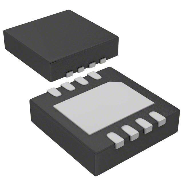
| 产品图片 |
|
| rohs | 符合RoHS无铅 / 符合限制有害物质指令(RoHS)规范要求 |
| 产品系列 | 电源管理 IC,低压差稳压器,Analog Devices ADP7104ACPZ-3.3-R7- |
| 数据手册 | |
| 产品型号 | ADP7104ACPZ-3.3-R7 |
| PCN组件/产地 | |
| PSRR/纹波抑制—典型值 | 50 dB |
| 产品种类 | 低压差稳压器 |
| 供应商器件封装 | 8-LFCSP-WD(3x3) |
| 其它名称 | ADP7104ACPZ-3.3-R7DKR |
| 包装 | Digi-Reel® |
| 商标 | Analog Devices |
| 回动电压—最大值 | 350 mV |
| 安装类型 | 表面贴装 |
| 安装风格 | SMD/SMT |
| 封装 | Reel |
| 封装/外壳 | 8-WFDFN 裸露焊盘,CSP |
| 封装/箱体 | LFCSP-8 |
| 工作温度 | -40°C ~ 85°C |
| 工厂包装数量 | 1500 |
| 最大工作温度 | + 125 C |
| 最大输入电压 | 20 V |
| 最小工作温度 | - 40 C |
| 最小输入电压 | 3.3 V |
| 标准包装 | 1 |
| 电压-跌落(典型值) | 0.35V @ 500mA |
| 电压-输入 | 最高 20V |
| 电压-输出 | 3.3V |
| 电流-输出 | 500mA |
| 电流-限制(最小值) | 625mA |
| 稳压器拓扑 | 正,固定式 |
| 稳压器数 | 1 |
| 系列 | ADP7104 |
| 线路调整率 | 0.015 % / V |
| 视频文件 | http://www.digikey.cn/classic/video.aspx?PlayerID=1364138032001&width=640&height=505&videoID=2245193149001 |
| 负载调节 | 0.2 % / A |
| 输入偏压电流—最大 | 10 nA |
| 输出电压 | 3.3 V |
| 输出电流 | 500 mA |
| 输出端数量 | 1 Output |
| 输出类型 | Fixed |
| 配用 | /product-detail/zh/EVAL-CN0276-SDPZ/EVAL-CN0276-SDPZ-ND/4571727/product-detail/zh/AD-FMCADC2-EBZ/AD-FMCADC2-EBZ-ND/4915055 |


PDF Datasheet 数据手册内容提取
20 V, 500 mA, Low Noise, CMOS LDO Data Sheet ADP7104 FEATURES TYPICAL APPLICATION CIRCUITS Input voltage range: 3.3 V to 20 V VIN = 8V VIN VOUT VOUT = 5V Maximum output current: 500 mA CIN + +COUT 1µF 1µF Low noise: 15 µV rms for fixed output versions SENSE PSRR performance of 60 dB at 10 kHz, VOUT = 3.3 V ON 10R01kΩ R10P0GkΩ Reverse current protection OFF EN/ UVLO Low dropout voltage: 350 mV at 500 mA 100kRΩ2 PG PG IAncictiuarla accyc uovraecry li: n±e0,. l8o%ad , and temperature: −2%/+1% GND 09507-001 Low quiescent current (VIN = 5 V), IGND = 900 μA with 500 mA load Figure 1. ADP7104 with Fixed Output Voltage, 5 V Low shutdown current: <40 µA at V = 12 V, stable with small IN 1 µF ceramic output capacitor VIN = 8V VIN VOUT VOUT = 5V 7 fixed output voltage options: 1.5 V, 1.8 V, 2.5 V, 3 V, 3.3 V, 1CµINF + 40.2kΩ +C1µOFUT ADJ 5 V, and 9 V R1 13kΩ Adjustable output from 1.22 V to VIN − VDO OFF ON 100kΩ EN/ R10P0GkΩ UVLO Foldback current limit and thermal overload protection R2 PG PG 100kΩ UP8o-slewerae dpr- rLgoFogCorSadPm i namdnadicb a8lte-ol epra redc SisOioICn pUaVcLkOag/eensa ble GND 09507-002 Figure 2. ADP7104 with Adjustable Output Voltage, 5 V APPLICATIONS Regulation to noise sensitive applications: ADC, DAC circuits, precision amplifiers, high frequency oscillators, clocks, and PLLs Communications and infrastructure Medical and healthcare Industrial and instrumentation GENERAL DESCRIPTION The ADP7104 is a CMOS, low dropout linear regulator that oper- The ADP7104 output noise voltage is 15 μV rms and is inde- ates from 3.3 V to 20 V and provides up to 500 mA of output pendent of the output voltage. A digital power-good output current. This high input voltage LDO is ideal for regulation of allows power system monitors to check the health of the output high performance analog and mixed signal circuits operating voltage. A user programmable precision undervoltage lockout from 19 V to 1.22 V rails. Using an advanced proprietary archi- function facilitates sequencing of multiple power supplies. tecture, it provides high power supply rejection, low noise, and The ADP7104 is available in 8-lead, 3 mm × 3 mm LFCSP achieves excellent line and load transient response with just a and 8-lead SOIC packages. The LFCSP offers a very compact small 1 µF ceramic output capacitor. solution and also provides excellent thermal performance for The ADP7104 is available in seven fixed output voltage options applications requiring up to 500 mA of output current in a and an adjustable version, which allows output voltages that range small, low-profile footprint. from 1.22 V to V − V via an external feedback divider. IN DO Rev. H Document Feedback Information furnished by Analog Devices is believed to be accurate and reliable. However, no responsibility is assumed by Analog Devices for its use, nor for any infringements of patents or other One Technology Way, P.O. Box 9106, Norwood, MA 02062-9106, U.S.A. rights of third parties that may result from its use. Specifications subject to change without notice. No license is granted by implication or otherwise under any patent or patent rights of Analog Devices. Tel: 781.329.4700 ©2011–2015 Analog Devices, Inc. All rights reserved. Trademarks and registered trademarks are the property of their respective owners. Technical Support www.analog.com
ADP7104 Data Sheet TABLE OF CONTENTS Features .............................................................................................. 1 Typical Performance Characteristics ..............................................7 Applications ....................................................................................... 1 Theory of Operation ...................................................................... 16 Typical Application Circuits ............................................................ 1 Applications Information .............................................................. 17 General Description ......................................................................... 1 Capacitor Selection .................................................................... 17 Revision History ............................................................................... 2 Programmable Undervoltage Lockout (UVLO) .................... 18 Specifications ..................................................................................... 3 Power-Good Feature .................................................................. 19 Input and Output Capacitor, Recommended Specifications ..... 4 Noise Reduction of the Adjustable ADP7104 ............................ 19 Absolute Maximum Ratings ............................................................ 5 Current Limit and Thermal Overload Protection ................. 20 Thermal Data ................................................................................ 5 Thermal Considerations ............................................................ 20 Thermal Resistance ...................................................................... 5 Printed Circuit Board Layout Considerations ............................ 23 ESD Caution .................................................................................. 5 Outline Dimensions ....................................................................... 24 Pin Configurations and Function Descriptions ........................... 6 Ordering Guide .......................................................................... 25 REVISION HISTORY 10/15—Rev. G to Rev. H Changes to Figure 59 and Figure 60 ............................................. 16 5/14—Rev. F to Rev. G Change to UVLO Threshold Rising Parameter, Table 1 ............. 4 Change to Power-Good Feature Section ..................................... 19 11/13—Rev. E to Rev. F Changes to Figure 53 through Figure 58 ..................................... 15 10/13—Rev. D to Rev. E Changes to Figure 1 and Figure 2 ................................................... 1 Changes to Figure 65 ...................................................................... 18 Changes to Figure 69 ...................................................................... 19 8/13—Rev. C to Rev. D Changes to Table 3 ............................................................................ 5 2/13—Rev. B to Rev. C Changes to Noise Reduction of the Adjustable ADP7104 Section .............................................................................................. 19 Updated Outline Dimensions ....................................................... 25 3/12—Rev. A to Rev. B Changes to Figure 66 ...................................................................... 18 11/11—Rev. 0 to Rev. A Changed Low Dropout Voltage from 200 mV to 350 mV .......... 1 Changes to Dropout Voltage Parameter ........................................ 3 10/11—Revision 0: Initial Version Rev. H | Page 2 of 25
Data Sheet ADP7104 SPECIFICATIONS V = (V + 1 V) or 3.3 V (whichever is greater), EN = V , I = 10 mA, C = C = 1 µF, T = 25°C, unless otherwise noted. IN OUT IN OUT IN OUT A Table 1. Parameter Symbol Conditions Min Typ Max Unit INPUT VOLTAGE RANGE V 3.3 20 V IN OPERATING SUPPLY CURRENT I I = 100 µA, V = 10 V 400 µA GND OUT IN I = 100 µA, V = 10 V, T = −40°C to +125°C 900 µA OUT IN J I = 10 mA, V = 10 V 450 µA OUT IN I = 10 mA, V = 10 V, T = −40°C to +125°C 1050 µA OUT IN J I = 300 mA, V = 10 V 750 µA OUT IN I = 300 mA, V = 10 V, T = −40°C to +125°C 1400 µA OUT IN J I = 500 mA, V = 10 V 900 µA OUT IN I = 500 mA, V = 10 V, T = −40°C to +125°C 1600 µA OUT IN J SHUTDOWN CURRENT I EN = GND, V = 12 V 40 50 µA GND-SD IN EN = GND, V = 12 V, T = −40°C to +125°C 75 µA IN J INPUT REVERSE CURRENT I EN = GND, V = 0 V, V = 20 V 0.3 µA REV-INPUT IN OUT EN = GND, V = 0 V, V = 20 V, T = −40°C to 5 µA IN OUT J +125°C OUTPUT VOLTAGE ACCURACY Fixed Output Voltage Accuracy V I = 10 mA –0.8 +0.8 % OUT OUT 1 mA < I < 500 mA, V = (V + 1 V) to 20 V, –2 +1 % OUT IN OUT T = −40°C to +125°C J Adjustable Output Voltage V I = 10 mA 1.21 1.22 1.23 V ADJ OUT Accuracy 1 mA < I < 500 mA, V = (V + 1 V) to 20 V, 1.196 1.232 V OUT IN OUT T = −40°C to +125°C J LINE REGULATION ∆V /∆V V = (V + 1 V) to 20 V, T = −40°C to +125°C −0.015 +0.015 %/V OUT IN IN OUT J LOAD REGULATION0F1 ∆VOUT/∆IOUT IOUT = 1 mA to 500 mA 0.2 %/A I = 1 mA to 500 mA, T = −40°C to +125°C 0.75 %/A OUT J ADJ INPUT BIAS CURRENT ADJ 1 mA < I < 500 mA, V = (V + 1 V) to 20 V, 10 nA I-BIAS OUT IN OUT ADJ connected to VOUT SENSE INPUT BIAS CURRENT SENSE 1 mA < I < 500 mA, V = (V + 1 V) to 20 V, 1 μA I-BIAS OUT IN OUT SENSE connected to VOUT, V = 1.5 V OUT DROPOUT VOLTAGE1F2 VDROPOUT IOUT = 10 mA 20 mV I = 10 mA, T = −40°C to +125°C 40 mV OUT J I = 150 mA 100 mV OUT I = 150 mA, T = −40°C to +125°C 175 mV OUT J I = 300 mA 200 mV OUT I = 300 mA, T = −40°C to +125°C 325 mV OUT J I = 500 mA 350 mV OUT I = 500 mA, T = −40°C to +125°C 550 mV OUT J START-UP TIME2F3 tSTART-UP VOUT = 5 V 1000 µs CURRENT-LIMIT THRESHOLD4 I 625 775 1000 mA 3F LIMIT PG OUTPUT LOGIC LEVEL PG Output Logic High PG I < 1 µA 1.0 V HIGH OH PG Output Logic Low PG I < 2 mA 0.4 V LOW OL PG OUTPUT THRESHOLD Output Voltage Falling PG −9.2 % FALL Output Voltage Rising PG −6.5 % RISE THERMAL SHUTDOWN Thermal Shutdown Threshold TSSD TJ rising 150 °C Thermal Shutdown Hysteresis TSSD-HYS 15 °C Rev. H | Page 3 of 25
ADP7104 Data Sheet Parameter Symbol Conditions Min Typ Max Unit PROGRAMMABLE EN/UVLO UVLO Threshold Rising UVLO 3.3 V ≤ V ≤ 20 V, T = −40°C to +125°C 1.18 1.22 1.28 V RISE IN J UVLO Threshold Falling UVLO 3.3 V ≤ V ≤ 20 V, T = −40°C to +125°C, 10 kΩ in 1.13 V FALL IN J series with the enable pin UVLO Hysteresis Current UVLO V > 1.25 V, T = −40°C to +125°C 7.5 9.8 12 µA HYS EN J Enable Pull-Down Current I EN = V 500 nA EN-IN IN Start Threshold V T = −40°C to +125°C 3.2 V START J Shutdown Threshold V T = −40°C to +125°C 2.45 V SHUTDOWN J Hysteresis 250 mV OUTPUT NOISE OUT 10 Hz to 100 kHz, V = 5.5 V, V = 1.8 V 15 µV rms NOISE IN OUT 10 Hz to 100 kHz, V = 6.3 V, V = 3.3 V 15 µV rms IN OUT 10 Hz to 100 kHz, V = 8 V, V = 5 V 15 µV rms IN OUT 10 Hz to 100 kHz, V = 12 V, V = 9 V 15 µV rms IN OUT 10 Hz to 100 kHz, V = 5.5 V, V = 1.5 V, 18 µV rms IN OUT adjustable mode 10 Hz to 100 kHz, V = 12 V, V = 5 V, 30 µV rms IN OUT adjustable mode 10 Hz to 100 kHz, V = 20 V, V = 15 V, 65 µV rms IN OUT adjustable mode POWER SUPPLY REJECTION RATIO PSRR 100 kHz, V = 4.3 V, V = 3.3 V 50 dB IN OUT 100 kHz, V = 6 V, V = 5 V 50 dB IN OUT 10 kHz, V = 4.3 V, V = 3.3 V 60 dB IN OUT 10 kHz, V = 6 V, V = 5 V 60 dB IN OUT 100 kHz, V = 3.3 V, V = 1.8 V, adjustable mode 50 dB IN OUT 100 kHz, V = 6 V, V = 5 V, adjustable mode 60 dB IN OUT 100 kHz, V = 16 V, V = 15 V, adjustable mode 60 dB IN OUT 10 kHz, V = 3.3 V, V = 1.8 V, adjustable mode 60 dB IN OUT 10 kHz, V = 6 V, V = 5 V, adjustable mode 80 dB IN OUT 10 kHz, V = 16 V, V = 15 V, adjustable mode 80 dB IN OUT 1 Based on an end-point calculation using 1 mA and 300 mA loads. See Figure 6 for typical load regulation performance for loads less than 1 mA. 2 Dropout voltage is defined as the input-to-output voltage differential when the input voltage is set to the nominal output voltage. This applies only for output voltages above 3.0 V. 3 Start-up time is defined as the time between the rising edge of EN to VOUT being at 90% of its nominal value. 4 Current limit threshold is defined as the current at which the output voltage drops to 90% of the specified typical value. For example, the current limit for a 5.0 V output voltage is defined as the current that causes the output voltage to drop to 90% of 5.0 V, or 4.5 V. INPUT AND OUTPUT CAPACITOR, RECOMMENDED SPECIFICATIONS Table 2. Parameter Symbol Conditions Min Typ Max Unit Minimum Input and Output Capacitance1 C T = −40°C to +125°C 0.7 µF 4F MIN A Capacitor ESR R T = −40°C to +125°C 0.001 0.2 Ω ESR A 1 The minimum input and output capacitance should be greater than 0.7 μF over the full range of operating conditions. The full range of operating conditions in the application must be considered during device selection to ensure that the minimum capacitance specification is met. X7R and X5R type capacitors are recommended; Y5V and Z5U capacitors are not recommended for use with any LDO. Rev. H | Page 4 of 25
Data Sheet ADP7104 ABSOLUTE MAXIMUM RATINGS on PCB material, layout, and environmental conditions. The Table 3. specified values of θ are based on a 4-layer, 4 in. × 3 in. circuit Parameter Rating JA board. See JESD51-7 and JESD51-9 for detailed information on VIN to GND −0.3 V to +22 V the board construction. For additional information, see the VOUT to GND −0.3 V to +20 V AN-617 Application Note, MicroCSP™ Wafer Level Chip Scale EN/UVLO to GND −0.3 V to VIN Package, available at www.analog.com. PG to GND −0.3 V to VIN SENSE/ADJ to GND −0.3 V to VOUT ΨJB is the junction-to-board thermal characterization parameter Storage Temperature Range −65°C to +150°C with units of °C/W. The package’s ΨJB is based on modeling and Operating Junction Temperature Range −40°C to +125°C calculation using a 4-layer board. The JESD51-12, Guidelines for Soldering Conditions JEDEC J-STD-020 Reporting and Using Electronic Package Thermal Information, states that thermal characterization parameters are not the same Stresses at or above those listed under Absolute Maximum as thermal resistances. ΨJB measures the component power Ratings may cause permanent damage to the product. This is a flowing through multiple thermal paths rather than a single stress rating only; functional operation of the product at these path as in thermal resistance, θJB. Therefore, ΨJB thermal paths or any other conditions above those indicated in the operational include convection from the top of the package as well as section of this specification is not implied. Operation beyond radiation from the package, factors that make ΨJB more useful the maximum operating conditions for extended periods may in real-world applications. Maximum junction temperature (TJ) affect product reliability. is calculated from the board temperature (TB) and power dissipation (P ) using the formula THERMAL DATA D T = T + (P × Ψ ) J B D JB Absolute maximum ratings apply individually only, not in combination. The ADP7104 can be damaged when the junction See JESD51-8 and JESD51-12 for more detailed information temperature limit is exceeded. Monitoring ambient temperature about ΨJB. does not guarantee that T is within the specified temperature J THERMAL RESISTANCE limits. In applications with high power dissipation and poor thermal resistance, the maximum ambient temperature may θJA and ΨJB are specified for the worst-case conditions, that is, a have to be derated. device soldered in a circuit board for surface-mount packages. θJC In applications with moderate power dissipation and low PCB is a parameter for surface-mount packages with top mounted thermal resistance, the maximum ambient temperature can heatsinks. θJC is presented here for reference only. exceed the maximum limit as long as the junction temperature Table 4. Thermal Resistance is within specification limits. The junction temperature (T) of the device is dependent on the ambient temperature (T ), tJhe Package Type θJA θJC ΨJB Unit A 8-Lead LFCSP 40.1 27.1 17.2 °C/W power dissipation of the device (P ), and the junction-to-ambient D 8-Lead SOIC 48.5 58.4 31.3 °C/W thermal resistance of the package (θ ). JA Maximum junction temperature (T) is calculated from the J ambient temperature (T ) and power dissipation (P ) using the ESD CAUTION A D formula T = T + (P × θ ) J A D JA Junction-to-ambient thermal resistance (θ ) of the package is JA based on modeling and calculation using a 4-layer board. The junction-to-ambient thermal resistance is highly dependent on the application and board layout. In applications where high maximum power dissipation exists, close attention to thermal board design is required. The value of θ may vary, depending JA Rev. H | Page 5 of 25
ADP7104 Data Sheet PIN CONFIGURATIONS AND FUNCTION DESCRIPTIONS VOUT1 8VIN VOUT 1 8 VIN SENSE/ADJ2 ADP7104 7PG SENSE/ADJ 2 ADP7104 7 PG TOP VIEW TOP VIEW GND3 (Not to Scale) 6GND GND 3 (Not to Scale) 6 GND NC4 5EN/UVLO NC 4 5 EN/UVLO NOTES NOTES 1. NC = NO CONNECT. DO NOT CONNECTTO 1. NC = NO CONNECT. DO NOT CONNECTTO THIS PIN. THIS PIN. 2.IT IS HIGHLY RECOMMENDED THAT THE 2.IT IS HIGHLY RECOMMENDED THAT THE EPPALXAPCNOKEAS EGODEN P BTAEHD EC OOBNNO NATEHRCEDT .BEODT TTOO MTH OEF G TRHOEUND 09507-003 EPPALXAPCNOKEAS EGODEN P BTAEHD EC OOBNNO NATEHRCEDT .BEODT TTOO MTH OEF G TRHOEUND 09507-004 Figure 3. LFCSP Package Figure 4. Narrow Body SOIC Package Table 5. Pin Function Descriptions Pin No. Mnemonic Description 1 VOUT Regulated Output Voltage. Bypass VOUT to GND with a 1 μF or greater capacitor. 2 SENSE/ADJ Sense (SENSE). Measures the actual output voltage at the load and feeds it to the error amplifier. Connect SENSE as close as possible to the load to minimize the effect of IR drop between the regulator output and the load. This function applies to fixed voltages only. Adjust Input (ADJ). An external resistor divider sets the output voltage. This function applies to adjustable voltages only. 3 GND Ground. 4 NC Do Not Connect to this Pin. 5 EN/UVLO Enable Input (EN). Drive EN high to turn on the regulator; drive EN low to turn off the regulator. For automatic startup, connect EN to VIN. Programmable Undervoltage Lockout (UVLO). When the programmable UVLO function is used, the upper and lower thresholds are determined by the programming resistors. 6 GND Ground. 7 PG Power Good. This open-drain output requires an external pull-up resistor to VIN or VOUT. If the part is in shutdown, current limit, thermal shutdown, or falls below 90% of the nominal output voltage, PG immediately transitions low. If the power-good function is not used, the pin may be left open or connected to ground. 8 VIN Regulator Input Supply. Bypass VIN to GND with a 1 μF or greater capacitor. EPAD Exposed Pad. Exposed paddle on the bottom of the package. The EPAD enhances thermal performance and is electrically connected to GND inside the package. It is highly recommended that the EPAD be connected to the ground plane on the board. Rev. H | Page 6 of 25
Data Sheet ADP7104 TYPICAL PERFORMANCE CHARACTERISTICS V = 7.5 V, V = 5 V, I = 10 mA, C = C = 1 µF, T = 25°C, unless otherwise noted. IN OUT OUT IN OUT A 3.35 1200 LOAD = 100µA LOAD = 100µA LOAD = 1mA LOAD = 1mA LOAD = 10mA LOAD = 10mA LOAD = 100mA 1000 LOAD = 100mA 3.33 LOAD = 300mA LOAD = 300mA LOAD = 500mA A) LOAD = 500mA µ T ( 800 V)3.31 REN (OUT CUR 600 V D 3.29 N U O 400 R G 3.27 200 3.25 0 –40°C –5°C T2J5 (°°CC) 85°C 125°C 09507-005 –40°C –5°C T2J5 (°°CC) 85°C 125°C 09507-008 Figure 5. Output Voltage vs. Junction Temperature Figure 8. Ground Current vs. Junction Temperature 3.35 800 700 3.33 A) 600 µ V)3.31 RENT ( 500 (OUT CUR 400 V D 3.29 N U 300 O R G 200 3.27 100 3.25 0 0.1 1 ILOAD10 (mA) 100 1000 09507-006 0.1 1 ILOAD10 (mA) 100 1000 09507-009 Figure 6. Output Voltage vs. Load Current Figure 9. Ground Current vs. Load Current 3.35 1200 LOAD = 100µA LOAD = 100µA LOAD = 1mA LOAD = 1mA LOAD = 10mA LOAD = 10mA LOAD = 100mA 1000 LOAD = 100mA 3.33 LOAD = 300mA LOAD = 300mA LOAD = 500mA A) LOAD = 500mA µ T ( 800 V)3.31 REN V (OUT D CUR 600 3.29 N U O 400 R G 3.27 200 3.254 6 8 10 VIN1 2(V) 14 16 18 20 09507-007 04 6 8 10 VIN1 2(V) 14 16 18 20 09507-010 Figure 7. Output Voltage vs. Input Voltage Figure 10. Ground Current vs. Input Voltage Rev. H | Page 7 of 25
ADP7104 Data Sheet 160 1400 3.3V 4.0V 140 68..00VV 1200 12.0V ENT (µA) 110200 20.0V NT (µA)1000 RR RE 800 U R C 80 U N C W D 600 DO 60 UN T O SHU 40 GR 400 LOAD = 5mA LOAD = 10mA 20 200 LLOOAADD == 120000mmAA LOAD = 300mA LOAD = 500mA 0–50 –25 0 TE2M5PERAT5U0RE (°C7)5 100 125 09507-011 03.1 3.2 3.3 VI3N. 4(V) 3.5 3.6 3.7 09507-014 Figure 11. Shutdown Current vs. Temperature at Various Input Voltages Figure 14. Ground Current vs. Input Voltage (in Dropout) 350 5.05 VOUT = 3.3V LOAD = 100µA TA = 25°C 5.04 LOAD = 1mA 300 LOAD = 10mA LOAD = 100mA 5.03 LOAD = 300mA LOAD = 500mA 250 5.02 V) m 5.01 OUT ( 200 (V)UT5.00 P O O 150 V R 4.99 D 100 4.98 4.97 50 4.96 01 10 ILOAD (mA) 100 1000 09507-012 4.95 –40°C –5°C T2J5 (°°CC) 85°C 125°C 09507-015 Figure 12. Dropout Voltage vs. Load Current Figure 15. Output Voltage vs. Junction Temperature, VOUT = 5 V 3.4 5.05 5.04 3.3 5.03 3.2 5.02 5.01 V) 3.1 V) (UT (UT5.00 O O V 3.0 V 4.99 2.9 4.98 LOAD = 5mA LOAD = 10mA 4.97 LOAD = 100mA 2.8 LOAD = 200mA LOAD = 300mA 4.96 LOAD = 500mA 2.7 4.95 3.1 3.2 3.3 VI3N. 4(V) 3.5 3.6 3.7 09507-013 0.1 1 ILOAD10 (mA) 100 1000 09507-016 Figure 13. Output Voltage vs. Input Voltage (in Dropout) Figure 16. Output Voltage vs. Load Current, VOUT = 5 V Rev. H | Page 8 of 25
Data Sheet ADP7104 5.05 300 LOAD = 100µA VOUT = 5V 5.04 LLOOAADD == 11m0mAA TA = 25°C LOAD = 100mA 250 5.03 LOAD = 300mA LOAD = 500mA 5.02 200 V) 5.01 m V (V)OUT45..9090 ROPOUT ( 150 D 100 4.98 4.97 50 4.96 4.956 8 10 12VIN (V)14 16 18 20 09507-017 01 10 ILOAD (mA) 100 1000 09507-018 Figure 17. Output Voltage vs. Input Voltage, VOUT = 5 V Figure 20. Dropout Voltage vs. Load Current, VOUT = 5 V 1000 5.05 LOAD = 100µA 900 LOAD = 1mA 5.00 LOAD = 10mA LOAD = 100mA 800 LOAD = 300mA 4.95 A) µ 700 4.90 T ( REN 600 V)4.85 D CUR 500 V (OUT4.80 N 400 4.75 U O R 300 4.70 G LOAD = 5mA 200 4.65 LOAD = 10mA LOAD = 100mA LOAD = 200mA 100 4.60 LOAD = 300mA LOAD = 500mA 0 4.55 –40°C –5°C T2J5 (°°CC) 85°C 125°C 09507-118 4.8 4.9 5.0 VI5N. 1(V) 5.2 5.3 5.4 09507-019 Figure 18. Ground Current vs. Junction Temperature, VOUT = 5 V Figure 21. Output Voltage vs. Input Voltage (in Dropout) 700 2500 600 2000 T (µA) 500 T (µA)1500 N N RE 400 RE R R U U1000 C C D 300 D N N U U O O 500 GR 200 GR LOAD = 5mA LOAD = 10mA 100 0 LOAD = 100mA LOAD = 200mA LOAD = 300mA LOAD = 500mA 0 –500 0.1 1 ILOAD10 (mA) 100 1000 09507-119 4.80 4.90 5.00 V5IN.1 (0V) 5.20 5.30 5.40 09507-020 Figure 19. Ground Current vs. Load Current, VOUT = 5 V Figure 22. Ground Current vs. Input Voltage (in Dropout), VOUT = 5 V Rev. H | Page 9 of 25
ADP7104 Data Sheet 1.85 900 LOAD = 100µA LOAD = 100µA LOAD = 1mA LOAD = 1mA LOAD = 10mA 800 LOAD = 10mA LOAD = 100mA LOAD = 100mA 1.83 LLOOAADD == 350000mmAA 700 LOAD = 300mA A) µ T ( 600 (V)UT1.81 URREN 500 VO D C 400 1.79 N U O 300 R G 1.77 200 100 1.75 0 –40°C –5°C T2J5 (°°CC) 85°C 125°C 09507-021 –40°C –5°C T2J5 (°°CC) 85°C 125°C 09507-126 Figure 23. Output Voltage vs. Junction Temperature, VOUT = 1.8 V Figure 26. Ground Current vs. Junction Temperature, VOUT = 1.8 V 1.85 700 600 1.83 A) 500 µ T ( 1.81 N (V)UT URRE 400 O C V1.79 ND 300 U O GR 200 1.77 100 1.750.1 1 ILOA1D0 (mA) 100 1000 09507-022 00.1 1 ILOAD1 0(mA) 100 1000 09507-127 Figure 24. Output Voltage vs. Load Current, VOUT = 1.8 V Figure 27. Ground Current vs. Load Current, VOUT = 1.8 V 1.85 1200 LOAD = 100µA LOAD = 100µA LOAD = 1mA LOAD = 1mA LOAD = 10mA LOAD = 10mA LOAD = 100mA 1000 LOAD = 100mA 1.83 LOAD = 300mA LOAD = 300mA LOAD = 500mA LOAD = 500mA A) µ T ( 800 (V)UT1.81 URREN 600 O C V D 1.79 N U O 400 R G 1.77 200 1.752 4 6 8 10VIN (V1)2 14 16 18 20 09507-023 02 4 6 8 10VIN (V1)2 14 16 18 20 09507-024 Figure 25. Output Voltage vs. Input Voltage, VOUT = 1.8 V Figure 28. Ground Current vs. Input Voltage, VOUT = 1.8 V Rev. H | Page 10 of 25
Data Sheet ADP7104 5.08 2.0 LOAD = 100µA 3.3V 5.07 LOAD = 1mA 4V LOAD = 10mA 5V LOAD = 100mA 6V 5.06 LOAD = 300mA A) 8V 5.05 LOAD = 500mA ENT (µ 1.5 111025VVV R 18V (V)OUT55..0034 WN CUR 1.0 20V V O 5.02 D T U 5.01 SH 5.00 OUT 0.5 I 4.99 4.98 –40°C –5°C T2J5 (°°CC) 85°C 125°C 09507-025 0–40 –20 0 20TEMP4E0RATU6R0E (°C8)0 100 120 140 09507-054 Figure 29. Output Voltage vs. Junction Temperature, VOUT = 5 V, Adjustable Figure 32. Reverse Input Current vs. Temperature, VIN = 0 V, Different Voltages on VOUT 5.08 0 LOAD = 500mA LOAD = 300mA 5.07 –10 LOAD = 100mA LOAD = 10mA 5.06 –20 LOAD = 1mA 5.05 –30 (V)UT55..0034 R (dB) ––5400 O R V S 5.02 P –60 5.01 –70 5.00 –80 4.99 –90 4.980.1 1 ILOAD10 (mA) 100 1000 09507-026 –10010 100 1kFREQU1E0NkCY (Hz)100k 1M 10M 09507-028 Figure 30. Output Voltage vs. Load Current, VOUT = 5 V, Adjustable Figure 33. Power Supply Rejection Ratio vs. Frequency, VOUT = 1.8 V, VIN = 3.3 V 5.08 0 LOAD = 500mA LOAD = 300mA 5.07 –10 LOAD = 100mA LOAD = 10mA LOAD = 1mA 5.06 –20 5.05 –30 V)5.04 dB) –40 V (OUT55..0023 PSRR ( ––6500 5.01 –70 LOAD = 100µA 5.00 LOAD = 1mA –80 LOAD = 10mA 4.99 LOAD = 100mA –90 LOAD = 300mA LOAD = 500mA 4.986 8 10 12VIN (V)14 16 18 20 09507-027 –10010 100 1kFREQU1E0NkCY (Hz)100k 1M 10M 09507-029 Figure 31. Output Voltage vs. Input Voltage, VOUT = 5 V, Adjustable Figure 34. Power Supply Rejection Ratio vs. Frequency, VOUT = 3.3 V, VIN = 4.8 V Rev. H | Page 11 of 25
ADP7104 Data Sheet 0 0 LOAD = 500mA LOAD = 500mA LOAD = 300mA LOAD = 300mA –10 LOAD = 100mA –10 LOAD = 100mA LOAD = 10mA LOAD = 10mA –20 LOAD = 1mA –20 LOAD = 1mA –30 –30 B) –40 B) –40 d d R ( –50 R ( –50 R R S S P –60 P –60 –70 –70 –80 –80 –90 –90 –10010 100 1kFREQU1E0NkCY (Hz)100k 1M 10M 09507-030 –10010 100 1kFREQU1E0NkCY (Hz)100k 1M 10M 09507-033 Figure 35. Power Supply Rejection Ratio vs. Frequency, VOUT = 3.3 V, VIN = 4.3 V Figure 38. Power Supply Rejection Ratio vs. Frequency, VOUT = 5 V, VIN = 6 V 0 0 LOAD = 500mA LOAD = 500mA LOAD = 300mA LOAD = 300mA –10 LOAD = 100mA –10 LOAD = 100mA LOAD = 10mA LOAD = 10mA –20 LOAD = 1mA –20 LOAD = 1mA –30 –30 B) –40 B) –40 R (d –50 R (d –50 R R S S P –60 P –60 –70 –70 –80 –80 –90 –90 –10010 100 1kFREQU1E0NkCY (Hz)100k 1M 10M 09507-031 –10010 100 1kFREQU1E0NkCY (Hz)100k 1M 10M 09507-034 Figure 36. Power Supply Rejection Ratio vs. Frequency, VOUT = 3.3 V, VIN = 3.8 V Figure 39. Power Supply Rejection Ratio vs. Frequency, VOUT = 5 V, VIN = 5.5 V 0 0 LOAD = 500mA LOAD = 500mA LOAD = 300mA LOAD = 300mA –10 LOAD = 100mA –10 LOAD = 100mA LOAD = 10mA LOAD = 10mA –20 LOAD = 1mA –20 LOAD = 1mA –30 –30 B) –40 B) –40 d d R ( –50 R ( –50 R R S S P –60 P –60 –70 –70 –80 –80 –90 –90 –10010 100 1kFREQU1E0NkCY (Hz)100k 1M 10M 09507-032 –10010 100 1kFREQU1E0NkCY (Hz)100k 1M 10M 09507-035 Figure 37. Power Supply Rejection Ratio vs. Frequency, VOUT = 5 V, VIN = 6.5 V Figure 40. Power Supply Rejection Ratio vs. Frequency, VOUT = 5 V, VIN = 5.3 V Rev. H | Page 12 of 25
Data Sheet ADP7104 0 0 LOAD = 500mA LOAD = 300mA –10 –10 LOAD = 100mA LOAD = 10mA –20 –20 LOAD = 1mA –30 –30 B) –40 B) –40 R (d –50 R (d –50 R R S S P –60 P –60 –70 –70 –80 –80 LOAD = 500mA LOAD = 300mA –90 LOAD = 100mA –90 LOAD = 10mA LOAD = 1mA –10010 100 1kFREQU1E0NkCY (Hz)100k 1M 10M 09507-036 –1000 0.25 H0E.5A0DROOM0. 7V5OLTAGE1. 0(V0) 1.25 1.50 09507-039 Figure 41. Power Supply Rejection Ratio vs. Frequency, VOUT = 5 V, VIN = 5.2 V Figure 44. Power Supply Rejection Ratio vs. Headroom Voltage, 100 Hz, VOUT = 5 V 0 0 LOAD = 500mA LOAD = 500mA LOAD = 300mA LOAD = 300mA –10 LOAD = 100mA –10 LOAD = 100mA LOAD = 10mA LOAD = 10mA LOAD = 1mA LOAD = 1mA –20 –20 –30 –30 B) –40 B) –40 d d R ( –50 R ( –50 R R S S P –60 P –60 –70 –70 –80 –80 –90 –90 –10010 100 1kFREQU1E0NkCY (Hz)100k 1M 10M 09507-037 –1000 0.25 H0E.5A0DROOM0. 7V5OLTAGE1. 0(V0) 1.25 1.50 09507-040 Figure 42. Power Supply Rejection Ratio vs. Frequency, VOUT = 5 V, VIN = 6 V Figure 45. Power Supply Rejection Ratio vs. Headroom Voltage, 1 kHz, Adjustable VOUT = 5 V 0 0 LOAD = 500mA LOAD = 500mA LOAD = 300mA LOAD = 300mA –10 LOAD = 100mA –10 LOAD = 100mA LOAD = 10mA LOAD = 10mA –20 LOAD = 1mA –20 LOAD = 1mA –30 –30 B) –40 B) –40 R (d –50 R (d –50 R R PS –60 PS –60 –70 –70 –80 –80 –90 –90 –10010 100 1kFREQU1E0NkCY (Hz)100k 1M 10M 09507-038 –1000 0.25 H0E.5A0DROOM0. 7V5OLTAGE1. 0(V0) 1.25 1.50 09507-041 Figure 43. Power Supply Rejection Ratio vs. Frequency, VOUT = 5 V, VIN = 6 V Figure 46. Power Supply Rejection Ratio vs. Headroom Voltage, 10 kHz, Adjustable With Noise Reduction Circuit VOUT = 5 V Rev. H | Page 13 of 25
ADP7104 Data Sheet 0 LOAD = 500mA –10 LLOOAADD == 310000mmAA LOAD CURRENT LOAD = 10mA LOAD = 1mA –20 1 –30 B) –40 d R ( –50 R S P –60 OUTPUT VOLTAGE 2 –70 –80 –90 –1000 0.25 H0E.5A0DROOM0. 7V5OLTAGE1. 0(V0) 1.25 1.50 09507-042 CH1 500mAΩBW CH2 50mV BW TM 1200%µs A CH1 270mA 09507-045 Figure 47. Power Supply Rejection Ratio vs. Headroom Voltage, 100 kHz, Figure 50. Load Transient Response, CIN, COUT = 1 μF, ILOAD = 1 mA to 500 mA, VOUT = 5 V VOUT = 1.8 V, VIN = 5 V 30 LOAD CURRENT 25 1 20 s) m V r E (µ 15 S NOI 2 OUTPUT VOLTAGE 10 3.3V 5 1.8V 5V 5VADJ 5VADJ NR 00.00001 0.0001 LO0.A00D1 CURREN0T.0 (1A) 0.1 1 09507-043 CH1500mAΩBW CH2 50mV BW TM 1200.µ2s% A CH1 280mA 09507-046 Figure 48. Output Noise vs. Load Current and Output Voltage, Figure 51. Load Transient Response, CIN, COUT = 1 μF, ILOAD = 1 mA to 500 mA, COUT = 1 μF VOUT = 3.3 V, VIN = 5 V 10 3.3V 5V LOAD CURRENT 5VADJ 5VADJ NR 1 1 Hz) √ V/ µ E ( S OI OUTPUT VOLTAGE N 2 0.1 0.0110 100 FREQUE1NkCY (Hz) 10k 100k 09507-044 CH1500mAΩBW CH2 50mV BW TM 1200.µ2s% A CH1 300mA 09507-047 Figure 49. Output Noise Spectral Density, ILOAD = 10 mA, COUT = 1 μF Figure 52. Load Transient Response, CIN, COUT = 1 μF, ILOAD = 1 mA to 500 mA, VOUT = 5 V, VIN = 7 V Rev. H | Page 14 of 25
Data Sheet ADP7104 INPUT VOLTAGE INPUT VOLTAGE 2 OUTPUT VOLTAGE 2 OUTPUT VOLTAGE 1 1 CH1 1V BW CH2 10mV BW TM 94.µ8s% A CH4 1.56V 09507-048 CH1 1VBW CH2 10mV BW TM 94.µ8s% A CH4 1.56V 09507-051 Figure 53. Line Transient Response, CIN, COUT = 1 μF, ILOAD = 500 mA, Figure 56. Line Transient Response, CIN, COUT = 1 μF, ILOAD = 1 mA, VOUT = 1.8 V VOUT = 1.8 V INPUT VOLTAGE INPUT VOLTAGE 2 OUTPUT VOLTAGE 2 OUTPUT VOLTAGE 1 1 CH1 1V BW CH2 10mV BW TM 94.µ8s% A CH4 1.56V 09507-049 CH1 1VBW CH2 10mV BW TM 94.µ8s% A CH4 1.56V 09507-052 Figure 54. Line Transient Response, CIN, COUT = 1 μF, ILOAD = 500 mA, Figure 57. Line Transient Response, CIN, COUT = 1 μF, ILOAD = 1 mA, VOUT = 3.3 V VOUT = 3.3 V INPUT VOLTAGE INPUT VOLTAGE 2 OUTPUT VOLTAGE 2 OUTPUT VOLTAGE 1 CH1 1V BW CH2 10mV BW TM 49µ.8s% A CH4 1.56V 09507-050 1 CH1 1VBW CH2 10mV BW TM 49µ.8s% A CH4 1.56V 09507-053 Figure 55. Line Transient Response, CIN, COUT = 1 μF, ILOAD = 500 mA, Figure 58. Line Transient Response, CIN, COUT = 1 μF, ILOAD = 1 mA, VOUT = 5 V VOUT = 5 V Rev. H | Page 15 of 25
ADP7104 Data Sheet THEORY OF OPERATION The ADP7104 is a low quiescent current, low-dropout linear feedback voltage is higher than the reference voltage, the gate regulator that operates from 3.3 V to 20 V and provides up to of the PMOS device is pulled higher, allowing less current to 500 mA of output current. Drawing a low 1 mA of quiescent pass and decreasing the output voltage. current (typical) at full load makes the ADP7104 ideal for The ADP7104 is available in seven fixed output voltage options, battery-operated portable equipment. Typical shutdown ranging from 1.5 V to 9 V and in an adjustable version with an current consumption is 40 μA at room temperature. output voltage that can be set to between 1.22 V and 19 V by an Optimized for use with small 1 µF ceramic capacitors, the external voltage divider. The output voltage can be set according ADP7104 provides excellent transient performance. to the following equation: V = 1.22 V(1 + R1/R2) VIN VOUT OUT GND VREG SHOTPRHRTEO-RCTMEIRCACTLUIT, PGOOD PG VIN = 8V 1CµINF + VIN VOAUDTJ 40.2kRΩ1 +C1µOFUT VOUT = 5V UVELNO/ 10µA SHUTDOWN SENSE OFF ON 10R03kΩR4 EUNV/LO 13kRΩ2 R10P0GkΩ 100kΩ REFERENCE 09507-056 GND PG PG 09507-075 Figure 59. Fixed Output Voltage Internal Block Diagram Figure 61. Typical Adjustable Output Voltage Application Schematic The value of R2 should be less than 200 kΩ to minimize errors VIN VOUT in the output voltage caused by the ADJ pin input current. For GND VREG SHORT-CIRCUIT, PGOOD PG example, when R1 and R2 each equal 200 kΩ, the output voltage THERMAL PROTECT is 2.44 V. The output voltage error introduced by the ADJ pin input current is 2 mV or 0.08%, assuming a typical ADJ pin input 10µA SHUTDOWN EN/ ADJ current of 10 nA at 25°C. UVLO The ADP7104 uses the EN/UVLO pin to enable and disable REF1E.R22EVNCE 09507-156 tEhNe /VUOVULOT pisi nh iugnhd, eVrO nUorTm taulr onps eornat, iwngh ecno nEdNit iios nlos.w W, VhOenU T turns off. For automatic startup, EN/UVLO can be tied to VIN. Figure 60. Adjustable Output Voltage Internal Block Diagram The ADP7104 incorporates reverse current protections circuitry Internally, the ADP7104 consists of a reference, an error amplifier, a that prevents current flow backwards through the pass element feedback voltage divider, and a PMOS pass transistor. Output when the output voltage is greater than the input voltage. A current is delivered via the PMOS pass device, which is controlled comparator senses the difference between the input and output by the error amplifier. The error amplifier compares the reference voltages. When the difference between the input voltage and voltage with the feedback voltage from the output and amplifies output voltage exceeds 55 mV, the body of the PFET is switched the difference. If the feedback voltage is lower than the reference to V and turned off or opened. In other words, the gate is voltage, the gate of the PMOS device is pulled lower, allowing OUT connected to VOUT. more current to pass and increasing the output voltage. If the Rev. H | Page 16 of 25
Data Sheet ADP7104 APPLICATIONS INFORMATION CAPACITOR SELECTION Figure 63 depicts the capacitance vs. voltage bias characteristic of an 0402, 1 µF, 10 V, X5R capacitor. The voltage stability of a Output Capacitor capacitor is strongly influenced by the capacitor size and voltage The ADP7104 is designed for operation with small, space-saving rating. In general, a capacitor in a larger package or higher voltage ceramic capacitors but functions with most commonly used rating exhibits better stability. The temperature variation of the capacitors as long as care is taken with regard to the effective series X5R dielectric is ~±15% over the −40°C to +85°C temperature resistance (ESR) value. The ESR of the output capacitor affects the range and is not a function of package or voltage rating. stability of the LDO control loop. A minimum of 1 µF capacitance 1.2 with an ESR of 1 Ω or less is recommended to ensure the stability of the ADP7104. Transient response to changes in load current is 1.0 also affected by output capacitance. Using a larger value of output capacitance improves the transient response of the ADP7104 to F) 0.8 µ large changes in load current. Figure 62 shows the transient E ( C responses for an output capacitance value of 1 µF. N A 0.6 T CI A P LOAD CURRENT CA 0.4 1 0.2 00 2 4VOLTAGE (V6) 8 10 09507-058 OUTPUT VOLTAGE 2 Figure 63. Capacitance vs. Voltage Characteristic Use Equation 1 to determine the worst-case capacitance accounting for capacitor variation over temperature, component tolerance, and voltage. CH1 500mAΩ CH2 50mV TM 1200%µs A CH1 270mA 09507-057 wherCe:E FF = CBIAS × (1 − TEMPCO) × (1 − TOL) (1) Figure 62. Output Transient Response, VOUT = 1.8 V, COUT = 1 µF C is the effective capacitance at the operating voltage. BIAS Input Bypass Capacitor TEMPCO is the worst-case capacitor temperature coefficient. Connecting a 1 µF capacitor from VIN to GND reduces TOL is the worst-case component tolerance. the circuit sensitivity to printed circuit board (PCB) layout, In this example, the worst-case temperature coefficient (TEMPCO) especially when long input traces or high source impedance over −40°C to +85°C is assumed to be 15% for an X5R dielectric. are encountered. If greater than 1 µF of output capacitance is The tolerance of the capacitor (TOL) is assumed to be 10%, and required, the input capacitor should be increased to match it. C is 0.94 μF at 1.8 V, as shown in Figure 63. BIAS Input and Output Capacitor Properties Substituting these values in Equation 1 yields Any good quality ceramic capacitors can be used with the CEFF = 0.94 μF × (1 − 0.15) × (1 − 0.1) = 0.719 μF ADP7104, as long as they meet the minimum capacitance and Therefore, the capacitor chosen in this example meets the maximum ESR requirements. Ceramic capacitors are manufac- minimum capacitance requirement of the LDO overtemper- tured with a variety of dielectrics, each with different behavior ature and tolerance at the chosen output voltage. over temperature and applied voltage. Capacitors must have a To guarantee the performance of the ADP7104, it is imperative dielectric adequate to ensure the minimum capacitance over that the effects of dc bias, temperature, and tolerances on the the necessary temperature range and dc bias conditions. X5R behavior of the capacitors be evaluated for each application. or X7R dielectrics with a voltage rating of 6.3 V to 25 V are recommended. Y5V and Z5U dielectrics are not recommended, due to their poor temperature and dc bias characteristics. Rev. H | Page 17 of 25
ADP7104 Data Sheet PROGRAMMABLE UNDERVOLTAGE LOCKOUT Hysteresis can also be achieved by connecting a resistor in (UVLO) series with EN/UVLO pin. For the example shown in Figure 65, the enable threshold is 2.44 V with a hysteresis of 1 V. The ADP7104 uses the EN/UVLO pin to enable and disable the VOUT pin under normal operating conditions. As shown in VIN = 8V VIN VOUT VOUT = 5V Figure 64, when a rising voltage on EN crosses the upper threshold, CIN + +COUT 1µF 1µF VOUT turns on. When a falling voltage on EN/ UVLO crosses SENSE R1 RPG the lower threshold, VOUT turns off. The hysteresis of the ON 100kΩ 100kΩ OFF EN/ EN/UVLO threshold is determined by the Thevenin equivalent UVLO R2 PG PG resistance in series with the EN/UVLO pin. 100kΩ 21..08 GND 09507-059 Figure 65. Typical EN Pin Voltage Divider 1.6 Figure 64 shows the typical hysteresis of the EN/UVLO pin. 1.4 This prevents on/off oscillations that can occur due to noise 1.2 on the EN pin as it passes through the threshold points. 1.0 VVOOUUTT,, EENN FRAISLEL The ADP7104 uses an internal soft-start to limit the inrush current 0.8 when the output is enabled. The start-up time for the 3.3 V option 0.6 is approximately 580 μs from the time the EN active threshold is 0.4 crossed to when the output reaches 90% of its final value. As shown in Figure 66, the start-up time is dependent on the 0.2 01.00 1.25 1.50 1.75 2.00 2.25 2.50 2.75 3.00 09507-060 output v6oltage setting. Figure 64. Typical VOUT Response to EN Pin Operation 5V The upper and lower thresholds are user programmable and can 5 be set using two resistors. When the EN/UVLO pin voltage is below 1.22 V, the LDO is disabled. When the EN/UVLO pin 4 voltage transitions above 1.22 V, the LDO is enabled and 10 µA V) 3.3V hysteresis current is sourced out the pin raising the voltage, thus (UT 3 O providing threshold hysteresis. Typically, two external resistors V program the minimum operational voltage for the LDO. The 2 ENABLE resistance values, R1 and R2 can be determined from: 1 R1 = V /10 μA HYS R2 = 1.22 V × R1/(V − 1.22 V) where: IN 00 500 TIM10E0 (0µs) 1500 2000 09507-061 VIN is the desired turn-on voltage. Figure 66. Typical Start-Up Behavior V is the desired EN/UVLO hysteresis level. HYS Rev. H | Page 18 of 25
Data Sheet ADP7104 POWER-GOOD FEATURE NOISE REDUCTION OF THE ADJUSTABLE ADP7104 The ADP7104 provides a power-good pin (PG) to indicate The ultralow output noise of the fixed output ADP7104 is the status of the output. This open-drain output requires an achieved by keeping the LDO error amplifier in unity gain external pull-up resistor to VIN or VOUT. If the part is in and setting the reference voltage equal to the output voltage. shutdown mode, current-limit mode, or thermal shutdown, or This architecture does not work for an adjustable output if it falls below 90% of the nominal output voltage, the power- voltage LDO. The adjustable output ADP7104 uses the more good pin (PG) immediately transitions low. During soft-start, conventional architecture where the reference voltage is fixed the rising threshold of the power-good signal is 93.5% of the and the error amplifier gain is a function of the output voltage. nominal output voltage. The disadvantage of the conventional LDO architecture is that the output voltage noise is proportional to the output voltage. The open-drain output is held low when the ADP7104 has suffi- cient input voltage to turn on the internal PG transistor. The PG The adjustable LDO circuit may be modified slightly to reduce transistor is terminated via a pull-up resistor to VOUT or VIN. the output voltage noise to levels close to that of the fixed output ADP7104. The circuit shown in Figure 69 adds two Power-good accuracy is 93.5% of the nominal regulator output additional components to the output voltage setting resistor voltage when this voltage is rising, with a 90% trip point when divider. C and R are added in parallel with R to reduce this voltage is falling. Regulator input voltage brownouts or NR NR FB1 the ac gain of the error amplifier. R is chosen to be equal to glitches trigger power no good signals if V falls below 90%. NR OUT R , this limits the ac gain of the error amplifier to approxi- FB2 A normal power-down causes the power-good signal to go low mately 6 dB. The actual gain is the parallel combination of R NR when V drops below 90%. OUT and R divided by R . This ensures that the error amplifier FB1 FB2 Figure 67 and Figure 68 show the typical power-good rising and always operates at greater than unity gain. falling threshold over temperature. C is chosen by setting the reactance of C equal to R − NR NR FB1 6 R at a frequency between 50 Hz and 100 Hz. This sets the PG –40°C NR PG –5°C frequency where the ac gain of the error amplifier is 3 dB PG +25°C 5 PG +85°C down from its dc gain. PG +125°C V) 4 VIN = 8V 1CµINF + VIN VOAUDTJ 40R.2FkBΩ1 +C10N0RnF +C1µOFUVTOUT = 5V PG ( 3 ON R1 RNR OFF 100kΩ EUNV/LO 1R3FkBΩ2 13kΩ R10P0GkΩ 2 R2 100kΩ 1 GND PG PG 09507-064 Figure 69. Noise Reduction Modification to Adjustable LDO 0 4.2 4.3 4.4 4.5 VOU4.T6 (V) 4.7 4.8 4.9 5.0 09507-062 The noise of the adjustable LDO is can be found by using the formula below assuming the noise of a fixed output LDO is Figure 67. Typical Power-Good Threshold vs. Temperature, VOUT Rising approximately 15 μV. 6 PG –40°C PG –5°C PG +25°C 1 5 PPGG ++81525°C°C 15μV× 1+1/13kΩ+1/40.2kΩ/13kΩ 4 Based on the component values shown in Figure 69, the V) ADP7104 has the following characteristics: G ( 3 P • DC gain of 4.09 (12.2 dB) 2 • 3 dB roll off frequency of 59 Hz • High frequency ac gain of 1.76 (4.89 dB) 1 • Noise reduction factor of 1.33 (2.59 dB) • RMS noise of the adjustable LDO without noise reduction 0 of 27.8 µV rms 4.2 4.3 4.4 4.5 VOU4.T6 (V) 4.7 4.8 4.9 5.0 09507-063 • RMS noise of the adjustable LDO with noise reduction Figure 68. Typical Power-Good Threshold vs. Temperature, VOUT Falling (assuming 15 µV rms for fixed voltage option) of 19.95 µV rms Rev. H | Page 19 of 25
ADP7104 Data Sheet CURRENT LIMIT AND THERMAL OVERLOAD To guarantee reliable operation, the junction temperature of PROTECTION the ADP7104 must not exceed 125°C. To ensure that the junction temperature stays below this maximum value, the The ADP7104 is protected against damage due to excessive user must be aware of the parameters that contribute to power dissipation by current and thermal overload protection junction temperature changes. These parameters include circuits. The ADP7104 is designed to current limit when the ambient temperature, power dissipation in the power device, output load reaches 600 mA (typical). When the output load and thermal resistances between the junction and ambient air exceeds 600 mA, the output voltage is reduced to maintain a (θ ). The θ number is dependent on the package assembly constant current limit. JA JA compounds that are used and the amount of copper used to Thermal overload protection is included, which limits the solder the package GND pins to the PCB. junction temperature to a maximum of 150°C (typical). Under Table 6 shows typical θ values of the 8-lead SOIC and 8-lead extreme conditions (that is, high ambient temperature and/or JA LFCSP packages for various PCB copper sizes. Table 7 shows high power dissipation) when the junction temperature starts to the typical Ψ values of the 8-lead SOIC and 8-lead LFCSP. rise above 150°C, the output is turned off, reducing the output JB current to zero. When the junction temperature drops below Table 6. Typical θ Values JA 135°C, the output is turned on again, and output current is θ (°C/W) JA restored to its operating value. Copper Size (mm2) LFCSP SOIC Consider the case where a hard short from VOUT to ground 251 165.1 167.8 occurs. At first, the ADP7104 current limits, so that only 600 mA 100 125.8 111 is conducted into the short. If self heating of the junction is 500 68.1 65.9 great enough to cause its temperature to rise above 150°C, 1000 56.4 56.1 thermal shutdown activates, turning off the output and reducing 6400 42.1 45.8 the output current to zero. As the junction temperature cools 1 Device soldered to minimum size pin traces. and drops below 135°C, the output turns on and conducts Table 7. Typical Ψ Values 600 mA into the short, again causing the junction temperature JB Model Ψ (°C/W) to rise above 150°C. This thermal oscillation between 135°C JB LFCSP 15.1 and 150°C causes a current oscillation between 600 mA and SOIC 31.3 0 mA that continues as long as the short remains at the output. Current and thermal limit protections are intended to protect The junction temperature of the ADP7104 is calculated from the the device against accidental overload conditions. For reliable following equation: operation, device power dissipation must be externally limited T = T + (P × θ ) (2) J A D JA so the junction temperature does not exceed 125°C. where: THERMAL CONSIDERATIONS T is the ambient temperature. A In applications with low input-to-output voltage differential, the PD is the power dissipation in the die, given by ADP7104 does not dissipate much heat. However, in applications P = [(V − V ) × I ] + (V × I ) (3) D IN OUT LOAD IN GND with high ambient temperature and/or high input voltage, the where: heat dissipated in the package may become large enough that I is the load current. it causes the junction temperature of the die to exceed the LOAD I is the ground current. maximum junction temperature of 125°C. GND V and V are input and output voltages, respectively. IN OUT When the junction temperature exceeds 150°C, the converter Power dissipation due to ground current is quite small and can enters thermal shutdown. It recovers only after the junction be ignored. Therefore, the junction temperature equation temperature has decreased below 135°C to prevent any permanent simplifies to the following: damage. Therefore, thermal analysis for the chosen application is very important to guarantee reliable performance over all TJ = TA + {[(VIN − VOUT) × ILOAD] × θJA} (4) conditions. The junction temperature of the die is the sum of As shown in Equation 4, for a given ambient temperature, input- the ambient temperature of the environment and the tempera- to-output voltage differential, and continuous load current, ture rise of the package due to the power dissipation, as shown there exists a minimum copper size requirement for the PCB in Equation 2. to ensure that the junction temperature does not rise above 125°C. Figure 70 to Figure 77 show junction temperature calculations for different ambient temperatures, power dissipation, and areas of PCB copper. Rev. H | Page 20 of 25
Data Sheet ADP7104 145 145 135 135 125 125 C) C) E (° 115 E (° 115 UR 105 UR 105 RAT 95 RAT 95 E E MP 85 MP 85 E E N T 75 N T 75 O O TI 65 TI 65 C C UN 55 UN 55 J J 45 6400mm2 45 6400mm2 500mm2 500mm2 35 25mm2 35 25mm2 TJMAX TJMAX 250 0.2 0.4 0.T6OT0A.8L P1O.0WE1R. 2DIS1S.4IPA1T.I6ON1 (.W8)2.0 2.2 2.4 09507-065 250 0.2 0.4 0.T6OT0A.8L P1O.0WE1R. 2DIS1S.4IPA1T.I6ON1 (.W8)2.0 2.2 2.4 09507-068 Figure 70. LFCSP, TA = 25°C Figure 73. SOIC, TA = 25°C 140 140 130 130 E (°C) 120 E (°C) 120 R R U 110 U 110 T T A A ER 100 ER 100 P P M M TE 90 TE 90 N N O O TI 80 TI 80 C C N N JU 70 JU 70 6400mm2 6400mm2 60 52050mmmm22 60 2550m0mmm22 TJMAX TJMAX 500 0.2 0.4TOTA0L.6 POW0E.8R DIS1S.0IPATI1O.2N (W)1.4 1.6 1.8 09507-066 500 0.2 0.4TOTA0L.6 POW0E.8R DIS1S.0IPATI1O.2N (W)1.4 1.6 1.8 09507-069 Figure 71. LFCSP, TA = 50°C Figure 74. SOIC, TA = 50°C 145 145 135 135 C) C) E (° 125 E (° 125 R R U U AT 115 AT 115 R R E E MP 105 MP 105 E E T T ON 95 ON 95 TI TI C C UN 85 UN 85 J J 6400mm2 6400mm2 75 500mm2 75 500mm2 25mm2 25mm2 TJMAX TJMAX 650 0.1 0.2TO0T.A3L P0O.W4ER0 D.5ISSIP0.A6TION0. 7(W)0.8 0.9 1.0 09507-067 650 0.1 0.2TO0T.A3L P0O.4WER0 D.5ISSI0P.A6TION0. 7(W)0.8 0.9 1.0 09507-070 Figure 72. LFCSP, TA = 85°C Figure 75. SOIC, TA = 85°C Rev. H | Page 21 of 25
ADP7104 Data Sheet 140 In the case where the board temperature is known, use the thermal characterization parameter, Ψ , to estimate the JB 120 junction temperature rise (see Figure 76 and Figure 77). )J T Maximum junction temperature (TJ) is calculated from E ( 100 R the board temperature (T ) and power dissipation (P ) U B D T A using the following formula: R 80 E P T = T + (P × Ψ ) (5) M J B D JB E T 60 The typical value of ΨJB is 15.1°C/W for the 8-lead LFCSP package ON and 31.3°C/W for the 8-lead SOIC package. CTI 40 N U 140 J TB = 25°C 20 TTBB == 5605°°CC 120 TB = 85°C TJMAX URE (T)J100 00 0.5 TO1.T0AL POW1.5ER DISS2.I0PATION2 (.W5) 3.0 3.5 09507-072 T A Figure 77. SOIC R 80 E P M E T 60 N O TI C 40 N U J TB = 25°C 20 TTBB == 5605°°CC TB = 85°C TJMAX 00 0.5 1.0 1.5TO2.T0AL2 .P5OW3.0ER3 D.5IS4S.I0PA4T.I5ON5 .(0W)5.5 6.0 6.5 7.0 09506-071 Figure 76. LFCSP Rev. H | Page 22 of 25
Data Sheet ADP7104 PRINTED CIRCUIT BOARD LAYOUT CONSIDERATIONS Heat dissipation from the package can be improved by increasing the amount of copper attached to the pins of the ADP7104. However, as listed in Table 6, a point of diminishing returns is eventually reached, beyond which an increase in the copper size does not yield significant heat dissipation benefits. Place the input capacitor as close as possible to the VIN and GND pins. Place the output capacitor as close as possible to the VOUT and GND pins. Use of 0805 or 0603 size capacitors and resistors achieves the smallest possible footprint solution on boards where area is limited. 09507-074 Figure 79. Example SOIC PCB Layout 09507-073 Figure 78. Example LFCSP PCB Layout Rev. H | Page 23 of 25
ADP7104 Data Sheet OUTLINE DIMENSIONS 3.10 2.48 3.00 SQ 2.38 2.90 2.23 5 8 EXPOSED 1.74 PAD 1.64 0.50 1.49 0.40 IANRDEEXA 0.30 4 1 0.20 MIN TOP VIEW BOTTOM VIEW PIN 1 INDICATOR 0.80 0.80 MAX (R 0.2) 0.55 NOM 0.75 FOR PROPER CONNECTION OF 0.70 0.05 MAX THE EXPOSED PAD, REFER TO 0.02 NOM THE PIN CONFIGURATION AND COPLANARITY FUNCTION DESCRIPTIONS 0.08 SECTION OF THIS DATA SHEET. SEPALTAINNGE 0.30 0.50 BSC 0.20 REF 0.25 0.18 COMPLIANTTOJEDEC STANDARDS MO-229-WEED-4 02-05-2013-B Figure 80. 8-Lead Lead Frame Chip Scale Package [LFCSP_WD] 3 mm × 3 mm Body, Very Very Thin, Dual Lead (CP-8-5) Dimensions shown in millimeters 5.00 3.098 4.90 4.80 0.356 8 5 6.20 4.00 6.00 3.90 5.80 2.41 3.80 0.457 1 4 FOR PROPER CONNECTION OF 1.27 BSC BOTTOM VIEW THE EXPOSED PAD, REFER TO 3.81 REF THE PIN CONFIGURATION AND FUNCTION DESCRIPTIONS TOP VIEW SECTION OF THIS DATA SHEET. 1.75 1.65 0.50 45° 1.35 1.25 0.25 0.25 0.17 0.10 MAX SEATING PLANE 0.51 0.05 NOM 8° 1.04 REF 0.31 COPL0A.1N0ARITY 0° 10..2470 COMPLIANTTO JEDEC STANDARDS MS-012-AA 06-03-2011-B Figure 81. 8-Lead Standard Small Outline Package, with Exposed Pad [SOIC_N_EP] Narrow Body (RD-8-2) Dimensions shown in millimeters Rev. H | Page 24 of 25
Data Sheet ADP7104 ORDERING GUIDE Temperature Output Package Package Model1 Range Voltage (V)2, 3 Description Option Branding 5F 6F 7F ADP7104ACPZ-R7 −40°C to +125°C Adjustable 8-Lead LFCSP_WD CP-8-5 LH1 ADP7104ACPZ-1.5-R7 −40°C to +125°C 1.5 8-Lead LFCSP_WD CP-8-5 LK6 ADP7104ACPZ-1.8-R7 −40°C to +125°C 1.8 8-Lead LFCSP_WD CP-8-5 LK7 ADP7104ACPZ-2.5-R7 −40°C to +125°C 2.5 8-Lead LFCSP_WD CP-8-5 LKJ ADP7104ACPZ-3.0-R7 −40°C to +125°C 3.0 8-Lead LFCSP_WD CP-8-5 LKK ADP7104ACPZ-3.3-R7 −40°C to +125°C 3.3 8-Lead LFCSP_WD CP-8-5 LKL ADP7104ACPZ-5.0-R7 −40°C to +125°C 5 8-Lead LFCSP_WD CP-8-5 LKM ADP7104ACPZ-9.0-R7 −40°C to +125°C 9 8-Lead LFCSP_WD CP-8-5 LLD ADP7104ARDZ-R7 −40°C to +125°C Adjustable 8-Lead SOIC_N_EP RD-8-2 ADP7104ARDZ-1.5-R7 −40°C to +125°C 1.5 8-Lead SOIC_N_EP RD-8-2 ADP7104ARDZ-1.8-R7 −40°C to +125°C 1.8 8-Lead SOIC_N_EP RD-8-2 ADP7104ARDZ-2.5-R7 −40°C to +125°C 2.5 8-Lead SOIC_N_EP RD-8-2 ADP7104ARDZ-3.0-R7 −40°C to +125°C 3.0 8-Lead SOIC_N_EP RD-8-2 ADP7104ARDZ-3.3-R7 −40°C to +125°C 3.3 8-Lead SOIC_N_EP RD-8-2 ADP7104ARDZ-5.0-R7 −40°C to +125°C 5 8-Lead SOIC_N_EP RD-8-2 ADP7104ARDZ-9.0-R7 −40°C to +125°C 9 8-Lead SOIC_N_EP RD-8-2 ADP7104CP-EVALZ 3.3 LFCSP Evaluation Board ADP7104RD-EVALZ 3.3 SOIC Evaluation Board ADP7104CPZ-REDYKIT LFCSP REDYKIT ADP7104RDZ-REDYKIT SOIC REDYKIT 1 Z = RoHS Compliant Part. 2 For additional voltage options, contact a local Analog Devices, Inc., sales or distribution representative. 3 The ADP7104CP-EVALZ and ADP7104RD-EVALZ evaluation boards are preconfigured with a 3.3 V ADP7104. ©2011–2015 Analog Devices, Inc. All rights reserved. Trademarks and registered trademarks are the property of their respective owners. D09507-0-10/15(H) Rev. H | Page 25 of 25
Mouser Electronics Authorized Distributor Click to View Pricing, Inventory, Delivery & Lifecycle Information: A nalog Devices Inc.: ADP7104ARDZ-R7 ADP7104ACPZ-5.0-R7 ADP7104ARDZ-5.0-R7 ADP7104ARDZ-1.8-R7 ADP7104ACPZ-3.3-R7 ADP7104ACPZ-R7 ADP7104ARDZ-3.3-R7 ADP7104ACPZ-3.0-R7 ADP7104ACPZ-2.5-R7 ADP7104ACPZ-9.0-R7 ADP7104ARDZ-1.5-R7 ADP7104ACPZ-1.8-R7 ADP7104ARDZ-9.0-R7 ADP7104ARDZ-3.0-R7 ADP7104ACPZ-1.5- R7 ADP7104ARDZ-2.5-R7