ICGOO在线商城 > 集成电路(IC) > PMIC - 稳压器 - 线性 > TPS71025DR
 Datasheet下载
- 型号: TPS71025DR
- 制造商: Texas Instruments
- 库位|库存: xxxx|xxxx
- 要求:
| 数量阶梯 | 香港交货 | 国内含税 |
| +xxxx | $xxxx | ¥xxxx |
查看当月历史价格
查看今年历史价格
TPS71025DR产品简介:
ICGOO电子元器件商城为您提供TPS71025DR由Texas Instruments设计生产,在icgoo商城现货销售,并且可以通过原厂、代理商等渠道进行代购。 TPS71025DR价格参考¥17.89-¥17.89。Texas InstrumentsTPS71025DR封装/规格:PMIC - 稳压器 - 线性, Linear Voltage Regulator IC Positive Fixed 1 Output 2.5V 500mA 8-SOIC。您可以下载TPS71025DR参考资料、Datasheet数据手册功能说明书,资料中有TPS71025DR 详细功能的应用电路图电压和使用方法及教程。
TPS71025DR是德州仪器(Texas Instruments)推出的一款低功耗、低压差线性稳压器(LDO),属于PMIC(电源管理集成电路)中的线性稳压器类别。以下是其主要应用场景:

 1. 便携式电子设备
TPS71025DR具有低静态电流(典型值为35μA)和小封装尺寸(SOT-23-5),非常适合对功耗和空间要求较高的便携式设备,例如:
- 手持终端
- 可穿戴设备(如智能手表、健康监测器)
- 便携式医疗设备(如血糖仪、脉搏血氧仪)

 2. 电池供电系统
由于其高效率和低功耗特性,TPS71025DR特别适用于电池供电的系统,能够延长电池寿命。典型应用包括:
- 无线传感器节点
- 遥控器
- 便携式音频设备

 3. 微控制器电源
TPS71025DR能够提供稳定的2.5V输出电压(±1%精度),非常适合为微控制器(MCU)及其外围电路供电。它支持高达200mA的负载电流,满足大多数低功耗MCU的需求。

 4. 通信模块
在物联网(IoT)设备中,TPS71025DR可以为低功耗蓝牙(BLE)、Wi-Fi或Zigbee等通信模块提供稳定的电源,确保信号传输的可靠性。

 5. 模拟和混合信号电路
TPS71025DR具有良好的电源抑制比(PSRR),能够有效滤除输入电源噪声,因此适合为以下电路供电:
- 数据转换器(ADC/DAC)
- 放大器
- 时钟振荡器

 6. 工业自动化
在工业环境中,TPS71025DR可用于为低功耗传感器、数据采集模块和控制单元供电,例如:
- 温度传感器
- 压力传感器
- 工业PLC模块

 7. 汽车电子(非关键功能)
尽管TPS71025DR不是车规级器件,但在某些非关键功能的应用中,它可以用于为汽车内部的低功耗设备供电,例如:
- 车载信息娱乐系统的辅助模块
- 环境监测传感器

 总结
TPS71025DR凭借其低功耗、小尺寸和高稳定性,广泛应用于对电源效率和空间要求较高的场景,尤其是在电池供电和低功耗系统中表现优异。
| 参数 | 数值 |
| 产品目录 | 集成电路 (IC) |
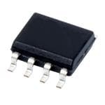
| 描述 | IC REG LDO 2.5V 0.5A 8SOIC |
| 产品分类 | |
| 品牌 | Texas Instruments |
| 数据手册 | |
| 产品图片 |
|
| 产品型号 | TPS71025DR |
| rohs | 无铅 / 符合限制有害物质指令(RoHS)规范要求 |
| 产品系列 | - |
| 产品目录页面 | |
| 供应商器件封装 | 8-SOIC |
| 其它名称 | 296-8043-6 |
| 包装 | Digi-Reel® |
| 安装类型 | 表面贴装 |
| 封装/外壳 | 8-SOIC(0.154",3.90mm 宽) |
| 工作温度 | 0°C ~ 125°C |
| 标准包装 | 1 |
| 电压-跌落(典型值) | 0.33V @ 500mA |
| 电压-输入 | 2.97 V ~ 10 V |
| 电压-输出 | 2.5V |
| 电流-输出 | 500mA |
| 电流-限制(最小值) | - |
| 稳压器拓扑 | 正,固定式 |
| 稳压器数 | 1 |


- 商务部:美国ITC正式对集成电路等产品启动337调查
- 曝三星4nm工艺存在良率问题 高通将骁龙8 Gen1或转产台积电
- 太阳诱电将投资9.5亿元在常州建新厂生产MLCC 预计2023年完工
- 英特尔发布欧洲新工厂建设计划 深化IDM 2.0 战略
- 台积电先进制程称霸业界 有大客户加持明年业绩稳了
- 达到5530亿美元!SIA预计今年全球半导体销售额将创下新高
- 英特尔拟将自动驾驶子公司Mobileye上市 估值或超500亿美元
- 三星加码芯片和SET,合并消费电子和移动部门,撤换高东真等 CEO
- 三星电子宣布重大人事变动 还合并消费电子和移动部门
- 海关总署:前11个月进口集成电路产品价值2.52万亿元 增长14.8%


PDF Datasheet 数据手册内容提取
TPS71025 LOW-DROPOUT VOLTAGE REGULATOR SLVS162A – MAY 1997 – REVISED MAY 1998 (cid:1) D OR P PACKAGE 2.5-V Fixed-Output Regulator (TOP VIEW) (cid:1) Very Low-Dropout (LDO) Voltage...57 mV Typical at IO = 100 mA GND 1 8 NC (cid:1) Very Low Quiescent Current, Independent EN 2 7 SENSE of Load...292 m A Typ IN 3 6 OUT (cid:1) IN 4 5 OUT Extremely Low Sleep-State Current, 0.5 m A Max (cid:1) 2% Tolerance Over Specified Conditions PW PACKAGE (cid:1) Output Current Range...0 mA to 500 mA (TOP VIEW) (cid:1) Available in Space Saving 8-Pin SOIC and GND 1 20 NC 20-Pin TSSOP Packages (cid:1) GND 2 19 NC 0°C to 125°C Operating Junction GND 3 18 NC Temperature Range NC 4 17 NC NC 5 16 NC description EN 6 15 SENSE The TPS71025 low-dropout regulator offers an NC 7 14 OUT order of magnitude reduction in both dropout IN 8 13 OUT voltage and quiescent current over conventional IN 9 12 NC LDO performance. The improvement results from IN 10 11 NC replacing the typical pnp pass transistor with a PMOS device. NC – No internal connection Because the PMOS device behaves as a low-value resistor, the dropout voltage is very low (maximum of 95mV at an output current of 100 mA) and is directly proportional to the output current (see Figure 1). Additionally, since the PMOS pass element is a voltage-driven device, the quiescent current is very low and remains independent of output loading (typically 292 m A over the full range of output current, 0 mA to 500mA). These two key specifications yield a significant improvement in operating life for battery-powered systems. The TPS71025 also features a sleep mode; applying a TTL high signal to EN (enable) shuts down the regulator, reducing the quiescent current to 0.5 m A maximum at T = 25°C. J AVAILABLE OPTIONS OUTPUT VOLTAGE PACKAGED DEVICES (V) CHIP FORM TTJJ SMALL OUTLINE PLASTIC DIP TSSOP (Y) MIN TYP MAX (D) (P) (PW) 0°C to 125°C 2.45 2.5 2.55 TPS71025D TPS71025P TPS71025PWLE TPS71025Y The D package is availabe taped and reeled. Add R suffix to device type (e.g., TPS71025DR). The PW package is only available left-end taped and reeled and is indicated by the LE suffix on the device type. Please be aware that an important notice concerning availability, standard warranty, and use in critical applications of TexasInstruments semiconductor products and disclaimers thereto appears at the end of this data sheet. PRODUCTION DATA information is current as of publication date. Copyright 1997, Texas Instruments Incorporated Products conform to specifications per the terms of Texas Instruments standard warranty. Production processing does not necessarily include testing of all parameters. POST OFFICE BOX 655303 • DALLAS, TEXAS 75265 1
TPS71025 LOW-DROPOUT VOLTAGE REGULATOR SLVS162A – MAY 1997 – REVISED MAY 1998 0.5 TA = 25°C 0.4 V – e 0.3 g a olt V ut o 0.2 p o r D 0.1 0 0 0.05 0.1 0.15 0.2 0.25 0.3 0.35 0.4 0.45 0.5 IO – Output Current – A Figure 1. Dropout Voltage Versus Output Current functional block diagram IN † † EN _ + Vref = 1.182 V OUT SENSE 260 kW 233 kW GND †Switch positions are shown with EN low (active). 2 POST OFFICE BOX 655303 • DALLAS, TEXAS 75265
TPS71025 LOW-DROPOUT VOLTAGE REGULATOR SLVS162A – MAY 1997 – REVISED MAY 1998 Terminal Functions TERMINAL NO. DESCRIPTION NNAAMMEE D or P PW EN 2 6 Enable input. Logic low enables output GND 1 1–3 Ground IN 3, 4 8–10 Input supply voltage OUT 5, 6 13, 14 Output voltage SENSE 7 15 Output voltage sense input TPS71025Y chip information These chips, when properly assembled, display characteristics similar to those of the TPS71025. Thermal compression or ultrasonic bonding may be used on the doped aluminum bonding pads. The chips may be mounted with conductive epoxy or a gold-silicon preform. BONDING PAD ASSIGNMENTS (3) (5) IN SENSE (5) (4) TPS71025 (2) (4) EN OUT (1) GND CHIP THICKNESS: 15 MILS TYPICAL 80 BONDING PADS: 4 × 4 MILS MINIMUM TJmax = 150°C TOLERANCES ARE ±10%. ALL DIMENSIONS ARE IN MILS. (1) (2) (3) NOTE A: For most applications, OUT and SENSE should be tied together as close as possible to the device; for other implementations, refer to SENSE-pin 92 connection discussion in the Application Information section of this data sheet. POST OFFICE BOX 655303 • DALLAS, TEXAS 75265 3
TPS71025 LOW-DROPOUT VOLTAGE REGULATOR SLVS162A – MAY 1997 – REVISED MAY 1998 absolute maximum ratings over operating free-air temperature range (unless otherwise noted)† Input voltage range, V, EN (see Note 1) . . . . . . . . . . . . . . . . . . . . . . . . . . . . . . . . . . . . . . . . . . . . . –0.3 V to 11 V I Continuous output current, I . . . . . . . . . . . . . . . . . . . . . . . . . . . . . . . . . . . . . . . . . . . . . . . . . . . . . . . . . . . . . . . . . 2 A O Continuous total power dissipation . . . . . . . . . . . . . . . . . . . . . . . . . . . . . See Dissipation Rating Tables 1 and 2 Operating virtual junction temperature range, T . . . . . . . . . . . . . . . . . . . . . . . . . . . . . . . . . . . . . . –0°C to 150°C J Storage temperature range, T . . . . . . . . . . . . . . . . . . . . . . . . . . . . . . . . . . . . . . . . . . . . . . . . . . . –65°C to 150°C stg Lead temperature 1,6 mm (1/16 inch) from case for 10 seconds . . . . . . . . . . . . . . . . . . . . . . . . . . . . . . . 260°C †Stresses beyond those listed under “absolute maximum ratings” may cause permanent damage to the device. These are stress ratings only, and functional operation of the device at these or any other conditions beyond those indicated under “recommended operating conditions” is not implied. Exposure to absolute-maximum-rated conditions for extended periods may affect device reliability. NOTE 1: All voltage values are with respect to GND DISSIPATION RATING TABLE 1 – FREE-AIR TEMPERATURE‡ TA ≤ 25°C DERATING FACTOR TA = 70°C TA = 125°C PACKAGE POWER RATING ABOVE TA = 25°C POWER RATING POWER RATING D 725 mW 5.8 mW/°C 464 mW 145 mW P 1175 mW 9.4 mW/°C 752 mW 235 mW PW 700 mW 5.6 mW/°C 448 mW 140 mW DISSIPATION RATING TABLE 2 – CASE TEMPERATURE‡ PPAACCKKAAGGEE TCC ≤ 25°C DERATING FACTOR TCC = 70°C TCC = 125°C POWER RATING ABOVE TC = 25°C POWER RATING POWER RATING D 2188 mW 17.5 mW/°C 1400 mW 438 mW P 2738 mW 21.9 mW/°C 1752 mW 548 mW PW 4025 mW 32.2 mW/°C 2576 mW 805 mW ‡Dissipation rating tables and figures are provided for maintenance of junction temperature at or below absolute maximum temperature of 150°C. For guidelines on maintaining junction temperature within recommended operating range, see the Thermal Information section. recommended operating conditions MIN MAX UNIT Input voltage, VI 2.97 10 V High-level input voltage at EN, VIH 2 V Low-level input voltage at EN, VIL 0 0.5 V Output current range, IO 0 500 mA Operating virtual junction temperature range, TJ 0 125 °C 4 POST OFFICE BOX 655303 • DALLAS, TEXAS 75265
TPS71025 LOW-DROPOUT VOLTAGE REGULATOR SLVS162A – MAY 1997 – REVISED MAY 1998 electrical characteristics over recommended operating junction temperature range, V = 3.5 V, I(IN) I = 10 mA, EN = 0 V, C = 4.7 m F/CSR† = 1 W , SENSE shorted to OUT (unless otherwise noted) O o PARAMETER TEST CONDITIONS‡ TJ MIN TYP MAX UNIT 25°C 2.5 OOuuttppuutt vvoollttaaggee 33.55 VV ≤≤ VVII ≤≤ 1100 VV 0°C to 125°C 2.45 2.55 VV 25°C 5.7 7.5 IIOO == 1100 mmAA, VVII == 22.4455 VV 0°C to 125°C 10 25°C 57 95 DDrrooppoouutt vvoollttaaggee IIOO == 110000 mmAA, VVII == 22.4455 VV 0°C to 125°C 105 mmVV 25°C 330 450 IIOO == 550000 mmAA, VVII == 22.4455 VV 0°C to 125°C 500 25°C 0.66 0.9 PPaassss-eelleemmeenntt sseerriieess rreessiissttaannccee WW 0°C to 125°C 1 VII = 3.5 V to 10 V, 25°C 7 23 IInnppuutt rreegguullaattiioonn 50 m A ≤ IO ≤ 500 mA 0°C to 125°C 12.7 29 mmVV IOO = 5 mA to 500 mA, 25°C 18 38 3.5 V ≤ VI ≤ 10 V 0°C to 125°C 75 mmVV OOuuttppuutt rreegguullaattiioonn IOO = 50 mm A to 500 mA, 25°C 24 60 3.5 V ≤ VI ≤ 10 V 0°C to 125°C 120 mmVV 25°C 43 53 ff == 112200 HHzz, IIOO == 5500 mm AA 0°C to 125°C 40 RRiippppllee rreejjeeccttiioonn ddBB 25°C 39 51 ff == 112200 HHzz, IIOO == 550000 mmAA 0°C to 125°C 36 Output noise-spectral density f = 120 Hz 25°C 2 m V/√Hz Co = 4.7 m F 25°C 274 1100 HHzz ≤≤ ff ≤≤ 110000kkHHzz, Output noise voltage CCSSRR == 11 WW Co = 10 m F 25°C 228 m Vrms Co = 100 m F 25°C 159 EN ≤ 0.5 V,, 25°C 292 390 QQuuiieesscceenntt ccuurrrreenntt ((aaccttiivvee mmooddee)) mm AA 0 mA ≤ IO ≤ 500 mA 0°C to 125°C 540 25°C 18 475 SSuuppppllyy ccuurrrreenntt ((ssttaannddbbyy mmooddee)) EENN == VVII, 22.77 VV ≤≤ VVII ≤≤ 1100 VV 0°C to 125°C 1900 nnAA 25°C 1.07 2 OOuuttppuutt ccuurrrreenntt lliimmiitt VVOO == 00, VVII == 1100 VV 0°C to 125°C 2 AA Pass-element leakagge current in standbyy 25°C 0.223 0.5 mode EENN == VVII, 22.77 VV ≤≤ VVII ≤≤ 1100 VV 0°C to 125°C 1 mm AA Output voltage temperature coefficient 0°C to 125°C 61 75 ppm/°C Thermal shutdown junction temperature 165 °C 2.5 V ≤ VI ≤ 6 V 25°C 2 LLooggiicc hhiigghh iinnppuutt vvoollttaaggee ((ssttaannddbbyy mmooddee)), EENN VV 6 V ≤ VI ≤ 10 V 0°C to 125°C 2.7 25°C 0.5 LLooggiicc llooww iinnppuutt vvoollttaaggee ((aaccttiivvee mmooddee)), EENN 22.77 VV ≤≤ VVII ≤≤ 1100 VV 0°C to 125°C 0.5 VV Hysteresis voltage, EN 0°C to 125°C 50 mV 25°C –0.5 0.5 IInnppuutt ccuurrrreenntt, EENN 00 VV ≤≤ VVII ≤≤ 1100 VV 0°C to 125°C –0.5 0.5 mm AA Input voltagge,, minimum for active pass 25°C 2 2.5 VV element 0°C to 125°C 2.5 †CSR (compensation series resistance) refers to the total series resistance, including the equivalent series resistance (ESR) of the capacitor, any series resistance added externally, and PWB trace resistance to Co. ‡Pulse-testing techniques are used to maintain virtual junction temperature as close as possible to ambient temperature; thermal effects must be taken into account separately. POST OFFICE BOX 655303 • DALLAS, TEXAS 75265 5
TPS71025 LOW-DROPOUT VOLTAGE REGULATOR SLVS162A – MAY 1997 – REVISED MAY 1998 electrical characteristics at T = 25°C, V = 3.5 V, I = 10 mA, EN = 0 V, C = 4.7 m F/CSR† = 1 W , J I(IN) O o SENSE shorted to OUT (unless otherwise noted) TPS71025Y PPAARRAAMMEETTEERR TTEESSTT CCOONNDDIITTIIOONNSS‡‡ UUNNIITT MIN TYP MAX Output voltage 3.5 V ≤ VI ≤ 10 V 2.5 V IO = 10 mA, VI = 2.45 V 5.7 Dropout voltage IO = 100 mA, VI = 2.45 V 57 mV IO = 500 mA, VI = 2.45 V 330 Pass-element series resistance 0.66 W Input regulation VI = 3.5 V to 10 V 7 mV IO = 5 mA to 500 mA 18 mV OOuuttppuutt rreegguullaattiioonn IO = 50 m A to 500 mA 24 mV f = 120 Hz, IO = 50 m A 53 RRiippppllee rreejjeeccttiioonn ddBB f = 120 Hz, IO = 500 mA 51 Output noise-spectral density f = 120 Hz 2 m V/√Hz Co = 4.7 m F 274 1100 HHz ≤≤ ff ≤≤ 110000 kkHHz, Output noise voltage CCSSRR == 11 WW Co = 10 m F 228 m Vrms Co = 100 m F 159 EN = 0 V, Quiescent current (active mode) 292 m A 0 mA ≤ IO ≤ 500 mA Supply current (standby mode) EN = VI, 2.7 V ≤ VI ≤ 10 V 18 nA Output current limit VO = 0, VI = 10 V 1.07 A Pass-element leakage current in standby mode EN = VI, 2.7 V ≤ VI ≤ 10 V 0.223 m A Output voltage temperature coefficient 61 ppm/°C Thermal shutdown junction temperature 165 °C 2.5 V ≤ VI ≤ 6 V 2 LLooggiicc hhiigghh iinnpputt voollttaaggee ((ssttaannddbby mmooddee)), EENN VV 6 V ≤ VI ≤ 10 V 2.7 Logic low input voltage (active mode), EN 2.7 V ≤ VI ≤ 10 V 0.5 V Hysteresis voltage, EN 50 mV Input current, EN 0 V ≤ VI ≤ 10 V 0 m A Input voltage, minimum for active pass element 2 V †CSR (compensation series resistance) refers to the total series resistance, including the equivalent series resistance (ESR) of the capacitor , any series resistance added externally, and PWB trace resistance to Co. ‡Pulse-testing techniques are used to maintain virtual junction temperature as close as possible to ambient temperature; thermal effects must be taken into account separately. 6 POST OFFICE BOX 655303 • DALLAS, TEXAS 75265
TPS71025 LOW-DROPOUT VOLTAGE REGULATOR SLVS162A – MAY 1997 – REVISED MAY 1998 TYPICAL CHARACTERISTICS OUTPUT VOLTAGE DROPOUT VOLTAGE vs vs FREE-AIR TEMPERATURE FREE-AIR TEMPERATURE 2.55 0.4 VI = 3.5 V VI = 2.45 V 2.54 0.35 2.53 IO = 500 mA 0.3 V age – 22..5521 e – V 0.25 olt ag ut V 2.5 IO = 10 mA Volt 0.2 utp 2.49 out O o 0.15 – rp O 2.48 D V IO = 500 mA 0.1 2.47 IO = 100 mA 0.05 2.46 IO = 10 mA 2.45 0 0 25 50 75 100 125 0 25 50 75 100 125 TA – Free-Air Temperature – °C TA – Free-Air Temperature – °C Figure 2 Figure 3 OUTPUT VOLTAGE OUTPUT VOLTAGE vs vs FREE-AIR TEMPERATURE INPUT VOLTAGE 2.55 2.55 2.54 IO = 5 mA 2.54 TA = 25°C IO = 500 mA 2.53 2.53 V V – 2.52 – 2.52 e e g g olta 2.51 olta 2.51 V V ut 2.5 ut 2.5 p p Out 2.49 Out 2.49 – – O 2.48 O 2.48 V V 2.47 2.47 2.46 2.46 2.45 2.45 0 25 50 75 100 125 3.5 4 4.5 5 5.5 6 6.5 7 7.5 8 8.5 9 9.5 10 TA – Free-Air Temperature – °C VI – Input Voltage – V Figure 4 Figure 5 POST OFFICE BOX 655303 • DALLAS, TEXAS 75265 7
TPS71025 LOW-DROPOUT VOLTAGE REGULATOR SLVS162A – MAY 1997 – REVISED MAY 1998 TYPICAL CHARACTERISTICS TYPICAL REGIONS OF STABILITY OUTPUT VOLTAGE COMPENSATION SERIES RESISTANCE vs vs OUTPUT CURRENT OUTPUT CURRENT 2.55 100 VI = 3.5 V 2.54 W– No Input Capacitance e Co = 4.7 m F c 2.53 n No Added Ceramic Capacitance a V st TA = 25°C – 2.52 si e e Region of Instability g R 10 Volta 2.51 eries put 2.5 n S Out 2.49 VI = 10 V atio – ns VO 2.48 VI = 3.5 V mpe 1 o 2.47 C – R 2.46 CS Region of Instability 2.45 0.1 0 100 200 300 400 500 0 50 100 150 200 250 300 350 400 450 500 IO – Output Current – mA IO – Output Current – mA Figure 6 Figure 7 TYPICAL REGIONS OF STABILITY TYPICAL REGIONS OF STABILITY COMPENSATION SERIES RESISTANCE COMPENSATION SERIES RESISTANCE vs vs OUTPUT CURRENT ADDED CERAMIC CAPACITANCE 100 100 VI = 3.5 V VI = 3.5 V W– No Input Capacitance W– No Input Capacitance ce Co = 4.7 m F + 0.5 m F of ce IO= 100 mA an Ceramic Capacitance an Co = 4.7 m F sist TA = 25°C sist TA = 25°C Re 10 Re 10 s Region of Instability s Region of Instability e e eri eri S S n n o o ati ati s s en 1 en 1 p p m m o o C C – – R R S Region of Instability S Region of Instability C C 0.1 0.1 0 50 100 150 200 250 300 350 400 450 500 0 0.1 0.2 0.3 0.4 0.5 0.6 0.7 0.8 0.9 1 IO – Output Current – mA Added Ceramic Capacitance – m F Figure 8 Figure 9 8 POST OFFICE BOX 655303 • DALLAS, TEXAS 75265
TPS71025 LOW-DROPOUT VOLTAGE REGULATOR SLVS162A – MAY 1997 – REVISED MAY 1998 TYPICAL CHARACTERISTICS TYPICAL REGIONS OF STABILITY TYPICAL REGIONS OF STABILITY† COMPENSATION SERIES RESISTANCE COMPENSATION SERIES RESISTANCE vs vs ADDED CERAMIC CAPACITANCE OUTPUT CURRENT 100 100 VI = 3.5 V Region of Instability VI = 3.5 V Wce – NIOo= I n50p0u tm CAapacitance We – NCoo I=n 1p0u tm CFapacitance Resistan 10 CTAo == 245.7° Cm F esistanc 10 NTAo =C e2r5a°mCic Capacitance es Region of Instability s R eri rie S e on n S sati atio n s e 1 n 1 p e m p m o C o CSR – Region of Instability CSR – C 0.1 0.1 0 0.1 0.2 0.3 0.4 0.5 0.6 0.7 0.8 0.9 1 0 50 100 150 200 250 300 350 400 450 500 Added Ceramic Capacitance – m F IO – Output Current – mA Figure 10 Figure 11 TYPICAL REGIONS OF STABILITY† TYPICAL REGIONS OF STABILITY† COMPENSATION SERIES RESISTANCE COMPENSATION SERIES RESISTANCE vs vs OUTPUT CURRENT ADDED CERAMIC CAPACITANCE 100 100 VI = 3.5 V VI = 3.5 V Wmpensation Series Resistance – 110 NCATAodo d=I=ne 21pd50u C° tmC eCFra a+pmR 0aei.cc5gi CtimoaaFnnp c ooaeffc iItnasntcaebility Wmpensation Series Resistance – 110 NCITOAoo = =I=n 1 21p050u0° tm C mCFAa Rpeagcioitnan ocfe Instability Co Co CSR – CSR – 0.1 0.1 0 50 100 150 200 250 300 350 400 450 500 0 0.1 0.2 0.3 0.4 0.5 0.6 0.7 0.8 0.9 1 IO – Output Current – mA Added Ceramic Capacitance – m F Figure 12 Figure 13 †CSR values below 0.1 W are not recommended. POST OFFICE BOX 655303 • DALLAS, TEXAS 75265 9
TPS71025 LOW-DROPOUT VOLTAGE REGULATOR SLVS162A – MAY 1997 – REVISED MAY 1998 TYPICAL CHARACTERISTICS TYPICAL REGIONS OF STABILITY† COMPENSATION SERIES RESISTANCE vs ADDED CERAMIC CAPACITANCE 100 VI = 3.5 V No Input Capacitance We – Co = 10 m F nc IO = 500 mA sta TA = 25°C si e 10 R s e Region of Instability ri e S n o ati s n 1 e p m o C – R S C 0.1 0 0.1 0.2 0.3 0.4 0.5 0.6 0.7 0.8 0.9 1 Added Ceramic Capacitance – m F †CSR values below 0.1 W are not recommended. Figure 14 To Load VI IN OUT + SENSE Co EN Ccer RL GND (see Note A) CSR NOTE A: Ceramic capacitor Figure 15. Test Circuit for Typical Regions of Stability (Figures 7 through 14) 10 POST OFFICE BOX 655303 • DALLAS, TEXAS 75265
TPS71025 LOW-DROPOUT VOLTAGE REGULATOR SLVS162A – MAY 1997 – REVISED MAY 1998 THERMAL INFORMATION In response to system-miniaturization trends, integrated circuits are being offered in low-profile and fine-pitch surface-mount packages. Implementation of many of today’s high-performance devices in these packages requires special attention to power dissipation. Many system-dependent issues such as thermal coupling, airflow, added heat sinks and convection surfaces, and the presence of other heat-generating components affect the power-dissipation limits of a given component. Three basic approaches for enhancing thermal performance are illustrated in this discussion: (cid:1) Improving the power-dissipation capability of the PWB design (cid:1) Improving the thermal coupling of the component to the PWB (cid:1) Introducing airflow in the system Figure 16 is an example of a thermally enhanced PWB layout for the 20-lead TSSOP package. This layout involves adding copper on the PWB to conduct heat away from the device. The Rq JA for this component/board system is illustrated in Figure 17. The family of curves illustrates the effect of increasing the size of the copper-heat-sink surface area. The PWB is a standard FR4 board (L × W × H = 3.2 inch × 3.2 inch × 0.062 inch); the board traces and heat sink area are 1-oz (per square foot) copper. Copper Heat Sink 1 oz Copper Figure 16. Thermally Enhanced PWB Layout (Not to Scale) for the 20-Pin TSSOP Figure 18 shows the thermal resistance for the same system with the addition of a thermally conductive compound between the body of the TSSOP package and the PWB copper routed directly beneath the device. The thermal conductivity for the compound used in this analysis is 0.815 W/m × °C. POST OFFICE BOX 655303 • DALLAS, TEXAS 75265 11
TPS71025 LOW-DROPOUT VOLTAGE REGULATOR SLVS162A – MAY 1997 – REVISED MAY 1998 THERMAL INFORMATION THERMAL RESISTANCE, JUNCTION-TO-AMBIENT THERMAL RESISTANCE, JUNCTION-TO-AMBIENT vs vs AIR FLOW AIR FLOW W W °C/ 190 Component/Board System °C/ 190 Component/Board System mbient – 170 1 cm2 20-L0 ecamd2 TSSOP mbient – 170 2ICn0oc-mLluepdaoedus Tn TSdh SeBOremPtwalelye nC Bonodduy catnivde Board A A mal Resistance, Junction-to- 11119350000 4 cm2 2 8c mcm22 mal Resistance, Junction-to- 11119350000 8 cm2 4 cm2 2 cm2 0 c1m c2m2 – TherA 7500 – TherA 7500 J 0 50 100 150 200 250 300 J 0 50 100 150 200 250 300 Rq Rq Air Flow – ft/min Air Flow – ft/min Figure 17 Figure 18 Using these figures to determine the system Rq JA allows the maximum power-dissipation PD(max) limit to be calculated with the equation: TJ(max)(cid:3)TA PD(max)(cid:4) R (cid:1)JA(system) Where TJ(max) is the maximum allowable junction temperature (i.e., 150°C absolute maximum or 125°C maximum recommended operating temperature for specified operation). This limit should then be applied to the internal power dissipated by the TPS71025 regulator. The equation for calculating total internal power dissipation of the device is: PD(total)(cid:4)(cid:5)VI(cid:3)VO(cid:6) (cid:1) IO(cid:2)(cid:5)VI (cid:1) IQ(cid:6) Because the quiescent current is very low, the second term is negligible, further simplifying the equation to: PD(total)(cid:4)(cid:5)VI(cid:3)VO(cid:6) (cid:1) IO 12 POST OFFICE BOX 655303 • DALLAS, TEXAS 75265
TPS71025 LOW-DROPOUT VOLTAGE REGULATOR SLVS162A – MAY 1997 – REVISED MAY 1998 THERMAL INFORMATION For a 20-lead TSSOP/FR4 board system with thermally conductive compound between the board and the device body, where T = 55°C, airflow = 100 ft/min, and copper heat sink area = 1 cm2, the maximum A power-dissipation limit can be calculated. As indicated in Figure 18, the system Rq JA is 94°C/W; therefore, the maximum power-dissipation limit is: PD(max)(cid:3)TRJ(cid:1)(JmAa(xs)ys(cid:2)teTmA) (cid:3)1259°4C°C(cid:2)(cid:4)W55°C(cid:3)745 mW If the system implements a TPS71025 regulator where V = 3.3 V and I = 385 mA, the internal power dissipation I O is: PD(total)(cid:3)(cid:5)VI(cid:2)VO(cid:6) (cid:1) IO(cid:3)(3.3(cid:2)2.5) (cid:1) 0.385(cid:3)308 mW Comparing P with P reveals that the power dissipation in this example does not exceed the D(total) D(max) maximum limit. When it does, one of two corrective actions can be taken. The power-dissipation limit can be raised by increasing the airflow or the heat-sink area. Alternatively, the internal power dissipation of the regulator can be lowered by reducing the input voltage or the load current. In either case, the above calculations should be repeated with the new system parameters. POST OFFICE BOX 655303 • DALLAS, TEXAS 75265 13
TPS71025 LOW-DROPOUT VOLTAGE REGULATOR SLVS162A – MAY 1997 – REVISED MAY 1998 APPLICATION INFORMATION TPS71025† 8 VI IN 15 9 SENSE IN 14 10 OUT VO IN C1 13 0.1 m F 6 EN OUT + Co 50 V 10 m F GND CSR 1 2 3 †Capacitor selection is nontrivial. See external capacitor requirements section. Figure 19. Typical Application Circuit The TPS71025 low-dropout (LDO) regulator overcomes many of the shortcomings of earlier-generation LDOs, while adding features such as a power-saving shutdown mode. device operation The TPS71025, unlike many other LDOs, features very low quiescent current that remains virtually constant even with varying loads. Conventional LDO regulators use a pnp-pass element, the base current of which is directly proportional to the load current through the regulator (I = I /b ). Examination of the data sheets reveals B C that those devices are typically specified under near no-load conditions; actual operating currents are much higher as evidenced by typical quiescent current versus load current curves. The TPS71025 uses a PMOS transistor to pass current; because the gate of the PMOS element is voltage driven, operating currents are low and stable over the full load range. The TPS71025 specifications reflect actual performance under load. Another pitfall associated with the pnp-pass element is its tendency to saturate when the device goes into dropout. The resulting drop in b forces an increase in I to maintain the load. During power up, this translates B to large start-up currents. Systems with limited supply current may fail to start up. In battery-powered systems, it means rapid battery discharge when the voltage decays below the minimum required for regulation. The TPS71025 quiescent current remains low even when the regulator drops out, eliminating both problems. The TPS71025 also features a shutdown mode that places the output in the high-impedance state (essentially equal to the feedback-divider resistance) and reduces quiescent current to under 2 m A. If the shutdown feature is not used, EN should be tied to ground. Response to an enable transition is quick; regulated output voltage is reestablished in typically 120 m s. minimum load requirements The TPS71025 family is stable even at zero load; no minimum load is required for operation. SENSE-pin connection The SENSE pin must be connected to the regulator output for proper functioning of the regulator. Normally, this connection should be as short as possible; however, the connection can be made near a critical circuit (remote sense) to improve performance at that point. Internally, SENSE connects to a high-impedance wide-bandwidth amplifier through a resistor-divider network, and noise pickup feeds through to the regulator output. Routing the SENSE connection to minimize/avoid noise pickup is essential. Adding an RC network between SENSE and OUT to filter noise is not recommended because it can cause the regulator to oscillate. 14 POST OFFICE BOX 655303 • DALLAS, TEXAS 75265
TPS71025 LOW-DROPOUT VOLTAGE REGULATOR SLVS162A – MAY 1997 – REVISED MAY 1998 APPLICATION INFORMATION external capacitor requirements An input capacitor is not required; however, a ceramic bypass capacitor (0.047 pF to 0.1 m F) improves load transient response and noise rejection if the TPS71025 is located more than a few inches from the power supply. A higher-capacitance electrolytic capacitor may be necessary if large (hundreds of milliamps) load transients with fast rise times are anticipated. As with most LDO regulators, the TPS71025 requires an output capacitor for stability. A low-ESR 10-m F solid-tantalum capacitor connected from the regulator output to ground is sufficient to ensure stability over the full load range (see Figure 11). Adding high-frequency ceramic or film capacitors (such as power-supply bypass capacitors for digital or analog ICs) can cause the regulator to become unstable unless the ESR of the tantalum capacitor is less than 1.2 W over temperature. Capacitors with published ESR specifications such as the AVX TPSD106K035R0300 and the Sprague 593D106X0035D2W work well because the maximum ESR at 25°C is 300 mW (typically, the ESR in solid-tantalum capacitors increases by a factor of 2 or less when the temperature drops from 25°C to –40°C). Where component height and/or mounting area is a problem, physically smaller, 10-m F devices can be screened for ESR. Figure 7 through Figure 14 show the stable regions of operation using different values of output capacitance with various values of ceramic load capacitance. In applications with little or no high-frequency bypass capacitance (< 0.2 m F), the output capacitance can be reduced to 4.7 m F, provided ESR is maintained between 0.7 and 2.5 W . Because minimum capacitor ESR is seldom if ever specified, it may be necessary to add a 0.5- W to 1-W resistor in series with the capacitor and limit ESR to 1.5 W maximum. As shown in the ESR graphs (Figure 7 through Figure 14), minimum ESR is not a problem when using 10-m F or larger output capacitors. Below is a partial listing of surface-mount capacitors usable with the TPS71025. This information (along with the ESR graphs, Figure 7 through Figure 14) is included to assist in selection of suitable capacitance for the application. When necessary to achieve low height requirements along with high output current and/or high ceramic load capacitance, several higher ESR capacitors can be used in parallel to meet the guidelines above. POST OFFICE BOX 655303 • DALLAS, TEXAS 75265 15
TPS71025 LOW-DROPOUT VOLTAGE REGULATOR SLVS162A – MAY 1997 – REVISED MAY 1998 APPLICATION INFORMATION external capacitor requirements (continued) All load and temperature conditions with up to 1 m F of added ceramic load capacitance: PART NO. MFR. VALUE MAX ESR† SIZE (H × L × W)† T421C226M010AS Kemet 22 m F, 10 V 0.5 2.8 × 6 × 3.2 593D156X0025D2W Sprague 15 m F, 25 V 0.3 2.8 × 7.3 × 4.3 593D106X0035D2W Sprague 10 m F, 35 V 0.3 2.8 × 7.3 × 4.3 TPSD106M035R0300 AVX 10 m F, 35 V 0.3 2.8 × 7.3 × 4.3 Load < 200 mA, ceramic load capacitance < 0.2 m F, full temperature range: PART NO. MFR. VALUE MAX ESR† SIZE (H × L × W)† 592D156X0020R2T Sprague 15 m F, 20 V 1.1 1.2 × 7.2 × 6 595D156X0025C2T Sprague 15 m F, 25 V 1 2.5 × 7.1 × 3.2 595D106X0025C2T Sprague 10 m F, 25 V 1.2 2.5 × 7.1 × 3.2 293D226X0016D2W Sprague 22 m F, 16 V 1.1 2.8 × 7.3 × 4.3 Load < 100 mA, ceramic load capacitance < 0.2 m F, full temperature range: PART NO. MFR. VALUE MAX ESR† SIZE (H × L × W)† 195D106X06R3V2T Sprague 10 m F, 6.3 V 1.5 1.3 × 3.5 × 2.7 195D106X0016X2T Sprague 10 m F, 16 V 1.5 1.3 × 7 × 2.7 595D156X0016B2T Sprague 15 m F, 16 V 1.8 1.6 × 3.8 × 2.6 695D226X0015F2T Sprague 22 m F, 15 V 1.4 1.8 × 6.5 × 3.4 695D156X0020F2T Sprague 15 m F, 20 V 1.5 1.8 × 6.5 × 3.4 695D106X0035G2T Sprague 10 m F, 35 V 1.3 2.5 × 7.6 × 2.5 †Size is in mm. ESR is maximum resistance at 100 kHz and TA = 25°C. Listings are sorted by height. 16 POST OFFICE BOX 655303 • DALLAS, TEXAS 75265
TPS71025 LOW-DROPOUT VOLTAGE REGULATOR SLVS162A – MAY 1997 – REVISED MAY 1998 MECHANICAL DATA D (R-PDSO-G**) PLASTIC SMALL-OUTLINE PACKAGE 14 PIN SHOWN PINS ** 0.050 (1,27) 8 14 16 DIM 0.020 (0,51) 0.010 (0,25) M 0.197 0.344 0.394 0.014 (0,35) A MAX (5,00) (8,75) (10,00) 14 8 0.189 0.337 0.386 A MIN (4,80) (8,55) (9,80) 0.244 (6,20) 0.228 (5,80) 0.008 (0,20) NOM 0.157 (4,00) 0.150 (3,81) Gage Plane 1 7 A 0.010 (0,25) 0°–8° 0.044 (1,12) 0.016 (0,40) Seating Plane 0.010 (0,25) 0.004 (0,10) 0.069 (1,75) MAX 0.004 (0,10) 4040047/D 10/96 NOTES: A. All linear dimensions are in inches (millimeters). B. This drawing is subject to change without notice. C. Body dimensions do not include mold flash or protrusion, not to exceed 0.006 (0,15). D. Falls within JEDEC MS-012 POST OFFICE BOX 655303 • DALLAS, TEXAS 75265 17
TPS71025 LOW-DROPOUT VOLTAGE REGULATOR SLVS162A – MAY 1997 – REVISED MAY 1998 MECHANICAL DATA P (R-PDIP-T8) PLASTIC DUAL-IN-LINE PACKAGE 0.400 (10,60) 0.355 (9,02) 8 5 0.260 (6,60) 0.240 (6,10) 1 4 0.070 (1,78) MAX 0.310 (7,87) 0.020 (0,51) MIN 0.290 (7,37) 0.200 (5,08) MAX Seating Plane 0.125 (3,18) MIN 0.100 (2,54) 0°–15° 0.021 (0,53) 0.010 (0,25) M 0.015 (0,38) 0.010 (0,25) NOM 4040082/B 03/95 NOTES: A. All linear dimensions are in inches (millimeters). B. This drawing is subject to change without notice. C. Falls within JEDEC MS-001 18 POST OFFICE BOX 655303 • DALLAS, TEXAS 75265
TPS71025 LOW-DROPOUT VOLTAGE REGULATOR SLVS162A – MAY 1997 – REVISED MAY 1998 MECHANICAL DATA PW (R-PDSO-G**) PLASTIC SMALL-OUTLINE PACKAGE 14 PIN SHOWN 0,30 0,65 0,10 M 0,19 14 8 0,15 NOM 4,50 6,60 4,30 6,20 Gage Plane 0,25 1 7 0°–8° A 0,75 0,50 Seating Plane 1,20 MAX 0,05 MIN 0,10 PINS ** 8 14 16 20 24 28 DIM A MAX 3,10 5,10 5,10 6,60 7,90 9,80 A MIN 2,90 4,90 4,90 6,40 7,70 9,60 4040064/E 08/96 NOTES: A. All linear dimensions are in millimeters. B. This drawing is subject to change without notice. C. Body dimensions do not include mold flash or protrusion not to exceed 0,15. D. Falls within JEDEC MO-153 POST OFFICE BOX 655303 • DALLAS, TEXAS 75265 19
PACKAGE OPTION ADDENDUM www.ti.com 6-Feb-2020 PACKAGING INFORMATION Orderable Device Status Package Type Package Pins Package Eco Plan Lead/Ball Finish MSL Peak Temp Op Temp (°C) Device Marking Samples (1) Drawing Qty (2) (6) (3) (4/5) TPS71025D ACTIVE SOIC D 8 75 Green (RoHS NIPDAU Level-1-260C-UNLIM 0 to 125 71025 & no Sb/Br) TPS71025DR ACTIVE SOIC D 8 2500 Green (RoHS NIPDAU Level-1-260C-UNLIM 0 to 125 71025 & no Sb/Br) TPS71025P ACTIVE PDIP P 8 50 Green (RoHS NIPDAU N / A for Pkg Type 0 to 125 TPS71025P & no Sb/Br) (1) The marketing status values are defined as follows: ACTIVE: Product device recommended for new designs. LIFEBUY: TI has announced that the device will be discontinued, and a lifetime-buy period is in effect. NRND: Not recommended for new designs. Device is in production to support existing customers, but TI does not recommend using this part in a new design. PREVIEW: Device has been announced but is not in production. Samples may or may not be available. OBSOLETE: TI has discontinued the production of the device. (2) RoHS: TI defines "RoHS" to mean semiconductor products that are compliant with the current EU RoHS requirements for all 10 RoHS substances, including the requirement that RoHS substance do not exceed 0.1% by weight in homogeneous materials. Where designed to be soldered at high temperatures, "RoHS" products are suitable for use in specified lead-free processes. TI may reference these types of products as "Pb-Free". RoHS Exempt: TI defines "RoHS Exempt" to mean products that contain lead but are compliant with EU RoHS pursuant to a specific EU RoHS exemption. Green: TI defines "Green" to mean the content of Chlorine (Cl) and Bromine (Br) based flame retardants meet JS709B low halogen requirements of <=1000ppm threshold. Antimony trioxide based flame retardants must also meet the <=1000ppm threshold requirement. (3) MSL, Peak Temp. - The Moisture Sensitivity Level rating according to the JEDEC industry standard classifications, and peak solder temperature. (4) There may be additional marking, which relates to the logo, the lot trace code information, or the environmental category on the device. (5) Multiple Device Markings will be inside parentheses. Only one Device Marking contained in parentheses and separated by a "~" will appear on a device. If a line is indented then it is a continuation of the previous line and the two combined represent the entire Device Marking for that device. (6) Lead/Ball Finish - Orderable Devices may have multiple material finish options. Finish options are separated by a vertical ruled line. Lead/Ball Finish values may wrap to two lines if the finish value exceeds the maximum column width. Important Information and Disclaimer:The information provided on this page represents TI's knowledge and belief as of the date that it is provided. TI bases its knowledge and belief on information provided by third parties, and makes no representation or warranty as to the accuracy of such information. Efforts are underway to better integrate information from third parties. TI has taken and continues to take reasonable steps to provide representative and accurate information but may not have conducted destructive testing or chemical analysis on incoming materials and chemicals. TI and TI suppliers consider certain information to be proprietary, and thus CAS numbers and other limited information may not be available for release. Addendum-Page 1
PACKAGE OPTION ADDENDUM www.ti.com 6-Feb-2020 In no event shall TI's liability arising out of such information exceed the total purchase price of the TI part(s) at issue in this document sold by TI to Customer on an annual basis. Addendum-Page 2
PACKAGE MATERIALS INFORMATION www.ti.com 20-Feb-2019 TAPE AND REEL INFORMATION *Alldimensionsarenominal Device Package Package Pins SPQ Reel Reel A0 B0 K0 P1 W Pin1 Type Drawing Diameter Width (mm) (mm) (mm) (mm) (mm) Quadrant (mm) W1(mm) TPS71025DR SOIC D 8 2500 330.0 12.4 6.4 5.2 2.1 8.0 12.0 Q1 PackMaterials-Page1
PACKAGE MATERIALS INFORMATION www.ti.com 20-Feb-2019 *Alldimensionsarenominal Device PackageType PackageDrawing Pins SPQ Length(mm) Width(mm) Height(mm) TPS71025DR SOIC D 8 2500 350.0 350.0 43.0 PackMaterials-Page2
IMPORTANTNOTICEANDDISCLAIMER TI PROVIDES TECHNICAL AND RELIABILITY DATA (INCLUDING DATASHEETS), DESIGN RESOURCES (INCLUDING REFERENCE DESIGNS), APPLICATION OR OTHER DESIGN ADVICE, WEB TOOLS, SAFETY INFORMATION, AND OTHER RESOURCES “AS IS” AND WITH ALL FAULTS, AND DISCLAIMS ALL WARRANTIES, EXPRESS AND IMPLIED, INCLUDING WITHOUT LIMITATION ANY IMPLIED WARRANTIES OF MERCHANTABILITY, FITNESS FOR A PARTICULAR PURPOSE OR NON-INFRINGEMENT OF THIRD PARTY INTELLECTUAL PROPERTY RIGHTS. These resources are intended for skilled developers designing with TI products. You are solely responsible for (1) selecting the appropriate TI products for your application, (2) designing, validating and testing your application, and (3) ensuring your application meets applicable standards, and any other safety, security, or other requirements. These resources are subject to change without notice. TI grants you permission to use these resources only for development of an application that uses the TI products described in the resource. Other reproduction and display of these resources is prohibited. No license is granted to any other TI intellectual property right or to any third party intellectual property right. TI disclaims responsibility for, and you will fully indemnify TI and its representatives against, any claims, damages, costs, losses, and liabilities arising out of your use of these resources. TI’s products are provided subject to TI’s Terms of Sale (www.ti.com/legal/termsofsale.html) or other applicable terms available either on ti.com or provided in conjunction with such TI products. TI’s provision of these resources does not expand or otherwise alter TI’s applicable warranties or warranty disclaimers for TI products. Mailing Address: Texas Instruments, Post Office Box 655303, Dallas, Texas 75265 Copyright © 2020, Texas Instruments Incorporated