ICGOO在线商城 > 集成电路(IC) > PMIC - 稳压器 - 线性 > SC4215HSETRT
 Datasheet下载
- 型号: SC4215HSETRT
- 制造商: SEMTECH
- 库位|库存: xxxx|xxxx
- 要求:
| 数量阶梯 | 香港交货 | 国内含税 |
| +xxxx | $xxxx | ¥xxxx |
查看当月历史价格
查看今年历史价格
SC4215HSETRT产品简介:
ICGOO电子元器件商城为您提供SC4215HSETRT由SEMTECH设计生产,在icgoo商城现货销售,并且可以通过原厂、代理商等渠道进行代购。 SC4215HSETRT价格参考。SEMTECHSC4215HSETRT封装/规格:PMIC - 稳压器 - 线性, Linear Voltage Regulator IC Positive Fixed or Adjustable 1 Output 0.5V, 0.5 V ~ 5.5 V 2A 8-SOIC-EP。您可以下载SC4215HSETRT参考资料、Datasheet数据手册功能说明书,资料中有SC4215HSETRT 详细功能的应用电路图电压和使用方法及教程。
Semtech Corporation的SC4215HSETRT是一款线性稳压器(PMIC),广泛应用于需要高效、低噪声电源管理的场景。以下是该型号的一些典型应用场景:

 1. 便携式电子设备
   SC4215HSETRT适用于便携式电子设备,如智能手机、平板电脑、可穿戴设备等。这些设备通常对功耗和空间有严格要求,而线性稳压器能够提供稳定的输出电压,确保设备在不同工作状态下保持性能稳定。其低噪声特性特别适合为音频、传感器等对电源质量敏感的模块供电。

 2. 物联网(IoT)设备
   在物联网设备中,如智能家居传感器、智能门锁、环境监测设备等,SC4215HSETRT可以为微控制器、无线通信模块等提供稳定的电源。由于这些设备通常依赖电池供电,因此低功耗和高效率的电源管理至关重要。SC4215HSETRT的高效能和小封装使其成为理想选择。

 3. 工业自动化与控制
   在工业环境中,SC4215HSETRT可以用于为各种传感器、执行器和通信接口供电。工业设备通常需要在恶劣环境下工作,因此电源的稳定性至关重要。线性稳压器的简单性和可靠性使其成为工业应用中的可靠选择,尤其是在需要长时间稳定运行的场合。

 4. 医疗设备
   医疗设备如便携式心率监测仪、血糖仪等,对电源的稳定性和安全性要求极高。SC4215HSETRT的低噪声和高效能特性使其非常适合为这些设备供电,确保测量结果的准确性。此外,其小尺寸封装也使得它能够在紧凑的设计中轻松集成。

 5. 汽车电子
   在汽车电子系统中,SC4215HSETRT可以用于为车载信息娱乐系统、传感器、摄像头等提供稳定的电源。汽车环境对电源的要求非常苛刻,线性稳压器的简单性和可靠性使其能够在宽温范围和振动环境下保持稳定工作。

总之,SC4215HSETRT凭借其高效、低噪声、小尺寸等特点,适用于多种对电源质量和功耗有严格要求的应用场景,特别是在便携式设备、物联网、工业自动化、医疗设备和汽车电子等领域表现尤为突出。
| 参数 | 数值 |
| 产品目录 | 集成电路 (IC) |
| 描述 | IC REG LDO ADJ 2A 8SOIC |
| 产品分类 | |
| 品牌 | Semtech |
| 数据手册 | |
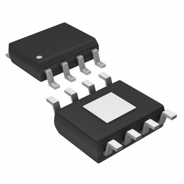
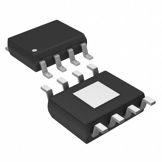
| 产品图片 |
|
| 产品型号 | SC4215HSETRT |
| rohs | 无铅 / 符合限制有害物质指令(RoHS)规范要求 |
| 产品系列 | - |
| 供应商器件封装 | 8-SOIC-EP |
| 其它名称 | SC4215HSETR |
| 包装 | 带卷 (TR) |
| 安装类型 | 表面贴装 |
| 封装/外壳 | 8-SOIC(0.154",3.90mm 宽)裸焊盘 |
| 工作温度 | -40°C ~ 105°C |
| 标准包装 | 2,500 |
| 电压-跌落(典型值) | 0.3V @ 2A |
| 电压-输入 | 1.4 V ~ 6 V |
| 电压-输出 | 可调至 0.5V |
| 电流-输出 | 2A |
| 电流-限制(最小值) | 2.1A |
| 稳压器拓扑 | 正,可调式 |
| 稳压器数 | 1 |


PDF Datasheet 数据手册内容提取
SC4215H Very Low Input /Very Low Dropout 2 Amp Regulator With Enable POWER MANAGEMENT Features Description Input Voltage as low as 1.4V The SC4215H is a high performance positive voltage regu- 400mV dropout @ 2A lator designed for use in applications requiring very low Adjustable output from 0.5V input voltage and very low dropout voltage at up to 2 Over current and over temperature protection amperes. It operates with a Vin as low as 1.4V, with output Enable pin voltage programmable as low as 0.5V. The SC4215H fea- 10µA quiescent current in shutdown tures ultra low dropout, ideal for applications where Vout Full industrial temperature range is very close to Vin. Additionally, the SC4215H has an Available in SOIC-8-EDP Lead-free package, fully WEEE enable pin to further reduce power dissipation while shut- and RoHS compliant and halogen free down. The SC4215H provides excellent regulation over variations in line, load and temperature. Applications The SC4215H is available in the SOIC-8-EDP (Exposed Die Pad) package. The output voltage can be set via an exter- Telecom/Networking cards nal divider or to a fixed setting of 0.5V depending on how Motherboards/Peripheral cards the FB pin is configured. Industrial applications Wireless infrastructure Set top boxes Medical equipment Notebook computers Battery powered systems Typical Application Circuit Rev. 3.1 © 2016 Semtech Corporation 1
SC4215H Pin Configuration Marking Information SC4215HSETRC YYWW=Datecode (Example: 1601) #: Cu Wire Material XXXXX=Semtech Lot No. (Example 00101) Marking Information SC4215HSETRT Ordering Information Device Package SC4215HSETRT(1)(2) SOIC-8-EDP SC4215HSETRC(1)(2) SOIC-8-EDP SC4215HEVB Evaluation Board Notes: (1) Available in tape and reel only. A reel contains 2,500 devices. (2) Available in lead-free package only. Device is WEEE and RoHS compliant and halogen free. 2
SC4215H Absolute Maximum Ratings Recommended Operating Conditions VIN, EN, VO, FB to GND (V) ..................-0.3 to +7.0 VIN (V) ................................... 1.4 < V < 6.0 IN Power Dissipation ..................... Internally Limited Ambient Temperature Range (°C) ......... -40 < T < +105 A ESD Protection Level(1) (kV) ........................... 2 Junction Temperature Range (°C) ......... -40 < T < +125 J Maximum Output Current (A) .........................2 Thermal Information Thermal Resistance, Junction to Ambient(2) (°C/W) .... 36 Thermal Resistance, Junc to Case(2) (°C/W) ............ 5.5 Maximum Junction Temperature (°C) ..............+150 Storage Temperature Range (°C) ............ -65 to +150 Peak IR Reflow Temperature (10s to 30s) (°C) ...... +260 Exceeding the above specifications may result in permanent damage to the device or device malfunction. Operation outside of the parameters specified in the Electrical Characteristics section is not recommended. NOTES: (1) Tested according to JEDEC standard JESD22-A114-B. (2) Calculated from package in still air, mounted to 3” x 4.5”, 4 layer FR4 PCB with thermal vias under the exposed pad per JESD51 standards. Electrical Characteristics Unless specified: V = V , V = V , V = 1.40V to 6.0V, I = 10µA to 2A, T = 25° C. EN IN FB O IN O A Values in bold apply over the full operating temperature range. Parameter Symbol Conditions Min Typ Max Units VIN V = 3.3V, I = 0A 3 mA IN O Quiescent Current I Q V = 6.0V, V =0V 10 50 µA IN EN VO V = V + 0.5V, I = 10mA IN O O -2% +2% Output Voltage(1) V V = 1.8V, I = 0.8A, 0°C ≤ T = T ≤85°C V V (Fixed Voltage, V = V ) O IN O J A O FB O 1.40V ≤ V ≤ 6.0V, I = 10mA -3% +3% IN O Line Regulation(1) REG I =10mA 0.2 0.4 %/V (LINE) O Load Regulation(1) REG I =10mA to 2A 0.5 1.5 % (LOAD) O 3
SC4215H Electrical Characteristics (continued) Parameter Symbol Conditions Min Typ Max Units 1.4V ≤ V < 1.6V 90 400 IN I =1A O 1.6V ≤ V ≤ 6.0V 200 IN 1.4V ≤ V < 1.6V 200 500 IN Dropout Voltage(1)(2) V I =1.5A mV DO O 1.6V ≤ V ≤ 6.0V 300 IN 1.4V ≤ V < 1.6V 300 600 IN I = 2A O 1.6V ≤ V ≤ 6.0V 400 IN Minimum Load Current(3)(4) I 10 µA O Current Limit(4) I 2.1 3 4.4 A CL Feedback 0.495 0.505 Reference Voltage(1) V V = 3.3V, V = V , I =10mA 0.5 V REF IN FB OUT O 0.490 0.510 Feedback Pin Current(4) I V = V 80 200 nA ADJ FB REF EN Enable Pin Current I V = 0V, V =3.3V 1.5 10 µA EN EN IN V 1.6 IH Enable Pin Threshold V =3.3V V IN V 0.4 IL Over Temperature Protection High Trip Level T 160 OC HI Hysteresis T 10 OC HYST Notes: (1) Low duty cycle pulse testing with Kelvin connections required. (2) V = V -V when V decreases by 1.5% of its nominal output voltage with V = V +0.8V. DO IN O O IN O (3) Required to maintain regulation. Voltage set resistors R1 and R2 are usually utilized to meet this requirement. (4) Guaranteed by design. 4
SC4215H Typical Characteristics 5
SC4215H Pin Descriptions Pin # Pin Name Pin Function Enable Input. Pulling this pin below 0.4V turns the regulator off, reducing the quiescent current to 2 EN a fraction of its operating value. The device will be enabled if this pin is left open. Connect to VIN if not being used. Input voltage. For regulation at full load, the input to this pin must be between (VO+ 0.5V) and 6.0V. Minimum VIN = 1.4V. A large bulk capacitance should be placed closely to this pin to ensure 3 VIN that the input supply does not sag below 1.4V. Also a minimum of 4.7uF ceramic capacitor should be placed directly at this pin. The pin is the power output of the device. A minimum of 10uF capacitor should be placed directly 6 VO at this pin. When this pin connected to the Vo pin, the output voltage will be set at 0.5V. If external feedback 7 FB resistors are used, the output voltage will be determined by the resistor ratio (See Application Circuits on page 1): Reference ground. The GND pin and the exposed die pad must be connected together at the IC 8 GND pin. 1, 4, 5 NC No Connection. THERMAL PAD Pad for heatsinking purposes. Connect to ground plane using multiple vias. Block Diagram 6
SC4215H Applications Information (continued) Introduction ≤50kΩ). A suitable value for R2 can be chosen in the range The SC4215H is intended for applications where high of 1kΩ to 50kΩ. R1 can then be calculated from. current capability and very low dropout voltage are required. It provides a very simple, low cost solution that ((VV −−VV )) RR ==RR ⋅⋅ OO RREEFF uses very little PCB real estate. Additional features include 11 22 VV RREEFF an enable pin to allow for a very low power consumption standby mode, and a fully adjustable output. Enable: Pulling this pin below 0.4V turns the regulator off, The SC4215H is especially recommended for applications reducing the quiescent current to a fraction of its operat- where VO>3.8V, for lower output voltage requirements ing value. A pull up resistor up to 400kOhms should be the SC4215A can be considered. connected from this pin to the VIN pin in applications where supply voltages of Vin < 1.9V are required. For Component Selection applications with higher voltages than 1.9V, EN pin could Input capacitor: A large bulk capacitance ≥ 10µF/A be left open or connected to VIN. (output load) should be closely placed to the input supply pin of the SC4215H to ensure that Vin does not sag below Thermal Considerations 1.4V. Also a minimum of 4.7µF ceramic capacitor is recom- The power dissipation in the SC4215H is given by: mended to be placed directly next to the Vin pin. This P ≈ I x (V - V ) D O IN O allows for the device being some distance from any bulk capacitance on the rail. Additionally, input droop due to The allowable power dissipation will be dependant on the load transients is reduced, improving load transient thermal impedance achieved in the application. The derat- response. Additional capacitance may be added if required ing curve below is valid for the thermal impedance speci- by the application. fied in the Thermal Information section on page 3. Output capacitor: A minimum bulk capacitance of ≥ 10µF/A (output load), along with a 0.1µF ceramic decou- pling capacitor is recommended. Increasing the bulk capacitance will improve the overall transient response. The use of multiple lower value ceramic capacitors in par- allel to achieve the desired bulk capacitance will not cause stability issues. Although designed for use with ceramic output capacitors, the SC4215H is extremely tolerant of output capacitor ESR values and thus will also work com- fortably with tantalum output capacitors. Noise immunity: In very electrically noisy environments, it is recommended that 0.1µF ceramic capacitors be placed from IN to GND and OUT to GND as close to the device pins as possible. Internal voltage selection: By connecting the FB pin directly to the VO pin, the output voltage will be regulated to the 0.5V internal reference. External voltage selection resistors: The use of 1% resistors, and designing for a current flow ≥ 10µA is rec- ommended to ensure a well regulated output (thus R2 7
SC4215H Outline Drawing — SOIC-8-EDP-2 8
SC4215H Land Pattern — SOIC-8-EDP-2 9
SC4215H © Semtech 2016 All rights reserved. Reproduction in whole or in part is prohibited without the prior written consent of the copyright owner. The information presented in this document does not form part of any quotation or contract, is believed to be accurate and reliable and may be changed without notice. No liability will be accepted by the publisher for any conse- quence of its use. Publication thereof does not convey nor imply any license under patent or other industrial or intellec- tual property rights. Semtech assumes no responsibility or liability whatsoever for any failure or unexpected operation resulting from misuse, neglect improper installation, repair or improper handling or unusual physical or electrical stress including, but not limited to, exposure to parameters beyond the specified maximum ratings or operation outside the specified range. SEMTECH PRODUCTS ARE NOT DESIGNED, INTENDED, AUTHORIZED OR WARRANTED TO BE SUITABLE FOR USE IN LIFE- SUPPORT APPLICATIONS, DEVICES OR SYSTEMS OR OTHER CRITICAL APPLICATIONS. INCLUSION OF SEMTECH PRODUCTS IN SUCH APPLICATIONS IS UNDERSTOOD TO BE UNDERTAKEN SOLELY AT THE CUSTOMER’S OWN RISK. Should a customer purchase or use Semtech products for any such unauthorized application, the customer shall indemnify and hold Semtech and its officers, employees, subsidiaries, affiliates, and distributors harmless against all claims, costs damages and attorney fees which could arise. Notice: All referenced brands, product names, service names and trademarks are the property of their respective owners. Contact Information Semtech Corporation Power Management Products Division 200 Flynn Road, Camarillo, CA 93012 Phone: (805) 498-2111 Fax: (805) 498-3804 www.semtech.com 10