ICGOO在线商城 > 集成电路(IC) > PMIC - 稳压器 - 线性 > ADP1708ACPZ-R7
 Datasheet下载
- 型号: ADP1708ACPZ-R7
- 制造商: Analog
- 库位|库存: xxxx|xxxx
- 要求:
| 数量阶梯 | 香港交货 | 国内含税 |
| +xxxx | $xxxx | ¥xxxx |
查看当月历史价格
查看今年历史价格
ADP1708ACPZ-R7产品简介:
ICGOO电子元器件商城为您提供ADP1708ACPZ-R7由Analog设计生产,在icgoo商城现货销售,并且可以通过原厂、代理商等渠道进行代购。 ADP1708ACPZ-R7价格参考。AnalogADP1708ACPZ-R7封装/规格:PMIC - 稳压器 - 线性, Linear Voltage Regulator IC Positive Adjustable 1 Output 1A 8-LFCSP-WD (3x3)。您可以下载ADP1708ACPZ-R7参考资料、Datasheet数据手册功能说明书,资料中有ADP1708ACPZ-R7 详细功能的应用电路图电压和使用方法及教程。
ADP1708ACPZ-R7是Analog Devices Inc.推出的一款低噪声、低压差(LDO)线性稳压器,适用于对电源噪声敏感的高性能电子系统。其典型应用场景包括便携式设备、通信系统和精密模拟电路。

该器件输出电流可达300mA,具有超低静态电流(典型值40μA),非常适合电池供电设备,如智能手机、平板电脑和可穿戴设备,有助于延长电池续航时间。其极低的输出电压噪声(约28μV RMS)和高电源抑制比(PSRR)使其广泛应用于射频(RF)模块、无线收发器、GPS模块以及音频放大电路等对电源纯净度要求高的场合。

ADP1708ACPZ-R7采用固定输出电压设计,输出精度高达±2%,并具备过温保护和过流保护功能,提升了系统可靠性。其小型化的6引脚、2mm × 2mm DFN封装,节省PCB空间,适合高密度布局的现代电子产品。

此外,该稳压器支持快速瞬态响应,能够在负载快速变化时保持稳定的输出电压,因此也适用于微处理器、FPGA、传感器模块等数字逻辑电路的辅助电源管理。

综上所述,ADP1708ACPZ-R7凭借低噪声、高稳定性和小尺寸特点,广泛应用于移动通信、消费电子、工业控制及医疗便携设备中,是高性能电源管理的理想选择。
| 参数 | 数值 |
| 产品目录 | 集成电路 (IC)半导体 |
| 描述 | IC REG LDO ADJ 1A 8LFCSP低压差稳压器 1A CMOS Linear Reg |
| 产品分类 | |
| 品牌 | Analog Devices |
| 产品手册 | |
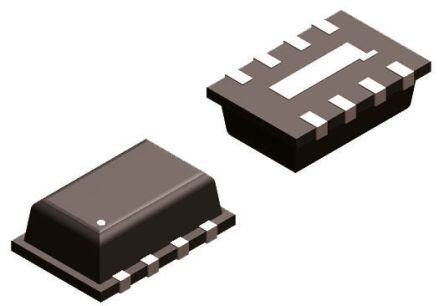
| 产品图片 |
|
| rohs | 符合RoHS无铅 / 符合限制有害物质指令(RoHS)规范要求 |
| 产品系列 | 电源管理 IC,低压差稳压器,Analog Devices ADP1708ACPZ-R7- |
| 数据手册 | |
| 产品型号 | ADP1708ACPZ-R7 |
| PCN其它 | |
| 产品培训模块 | http://www.digikey.cn/PTM/IndividualPTM.page?site=cn&lang=zhs&ptm=19143 |
| 产品种类 | 低压差稳压器 |
| 供应商器件封装 | 8-LFCSP-VD(3x3) |
| 其它名称 | ADP1708ACPZ-R7CT |
| 包装 | 剪切带 (CT) |
| 商标 | Analog Devices |
| 安装类型 | 表面贴装 |
| 安装风格 | SMD/SMT |
| 封装 | Reel |
| 封装/外壳 | 8-VFDFN 裸露焊盘,CSP |
| 封装/箱体 | LFCSP-8 |
| 工作温度 | -40°C ~ 125°C |
| 工厂包装数量 | 1500 |
| 最大工作温度 | + 125 C |
| 最大输入电压 | 5.5 V |
| 最小工作温度 | - 40 C |
| 最小输入电压 | 2.5 V |
| 标准包装 | 1 |
| 电压-跌落(典型值) | 0.345V @ 1A |
| 电压-输入 | 2.5 V ~ 5.5 V |
| 电压-输出 | 0.8 V ~ 5 V |
| 电流-输出 | 1A |
| 电流-限制(最小值) | 1.1A |
| 稳压器拓扑 | 正,可调式 |
| 稳压器数 | 1 |
| 系列 | ADP1708 |
| 视频文件 | http://www.digikey.cn/classic/video.aspx?PlayerID=1364138032001&width=640&height=505&videoID=2245193149001 |
| 输出电流 | 1 A |
| 配用 | /product-detail/zh/ADP1708-EVALZ/ADP1708-EVALZ-ND/1805675 |


- 商务部:美国ITC正式对集成电路等产品启动337调查
- 曝三星4nm工艺存在良率问题 高通将骁龙8 Gen1或转产台积电
- 太阳诱电将投资9.5亿元在常州建新厂生产MLCC 预计2023年完工
- 英特尔发布欧洲新工厂建设计划 深化IDM 2.0 战略
- 台积电先进制程称霸业界 有大客户加持明年业绩稳了
- 达到5530亿美元!SIA预计今年全球半导体销售额将创下新高
- 英特尔拟将自动驾驶子公司Mobileye上市 估值或超500亿美元
- 三星加码芯片和SET,合并消费电子和移动部门,撤换高东真等 CEO
- 三星电子宣布重大人事变动 还合并消费电子和移动部门
- 海关总署:前11个月进口集成电路产品价值2.52万亿元 增长14.8%


PDF Datasheet 数据手册内容提取
1 A, Low Dropout, CMOS Linear Regulator Data Sheet ADP1706/ADP1707/ADP1708 FEATURES TYPICAL APPLICATION CIRCUITS Maximum output current: 1 A ADP1706 10nF Input voltage range: 2.5 V to 5.5 V 1 EN SS 8 Low shutdown current: <1 µA 2 GND SENSE 7 Low dropout voltage: 345 mV at 1 A load VIN = 5V 3 IN OUT 6 VOUT = 3.3V IAncictiuarla accyc ouvraecry li:n ±e1,% lo ad, and temperature: ±2.5% 4.7µF 4 IN OUT 5 4.7µF 06640-001 16 fixed output voltage options with soft start Figure 1. ADP1706 with Fixed Output Voltage, 3.3 V 0.75 V to 3.3 V (ADP1706) ADP1707 16 fixed output voltage options with tracking 1 EN TRK 8 VTRK 0.75 V to 3.3 V (ADP1707) 2 GND SENSE 7 Adjustable output voltage option VIN = 5V 3 IN OUT 6 VOUT 0.8 V to 5.0 V (ADP1708) 4 IN OUT 5 Stable with small 4.7 µF ceramic output capacitor 4.7µF 4.7µF Excellent load/line transient response VOUT (V) 3 Current limit and thermal overload protection 2 Logic-controlled enable 1 Avaa i3la mblme i×n 3a nm 8m-l,e 8a-dle, aedx peoxspeods epda dpdalded SleO LICF CaSnPd 0 1V2TRK3 (4V)5 06640-003 Figure 2. ADP1707 with Output Voltage Tracking APPLICATIONS ADP1708 R2 Notebook computers Memory components 1 EN ADJ 8 R1 2 GND SENSE 7 Telecommunications equipment VIN = 5V 3 IN OUT 6 VOUT = 0.8V(1 + R1/R2) Network equipment DInSsPtr/uFmPGeAn/tmatiicorno peqrouciepsmsoern st/udpaptlai easc quisition systems 4.7µF 4 IN OUT 5 4.7µF 06640-002 Figure 3. ADP1708 with Adjustable Output Voltage, 0.8 V to 5.0 V GENERAL DESCRIPTION The ADP1706/ADP1707/ADP1708 are CMOS, low dropout ADP1707 and ADP1708 contain internal soft start capacitors linear regulators that operate from 2.5 V to 5.5 V and provide that give a typical start-up time of 100 µs. The ADP1707 up to 1 A of output current. Using an advanced proprietary includes a tracking feature that allows the output to follow an architecture, they provide high power supply rejection and external voltage rail or reference. achieve excellent line and load transient response with a small The ADP1706/ADP1707/ADP1708 are available in an 8-lead, 4.7 µF ceramic output capacitor. exposed paddle SOIC package and an 8-lead, 3 mm × 3 mm The ADP1706/ADP1707 are available in 16 fixed output voltage exposed paddle LFCSP, making them not only very compact options. The ADP1708 is available in an adjustable version, solutions but also providing excellent thermal performance for which allows output voltages that range from 0.8 V to 5.0 V via applications requiring up to 1 A of output current in a small, an external divider. The ADP1706 allows an external soft start low profile footprint. capacitor to be connected to program the start-up time; the Rev. A Document Feedback Information furnished by Analog Devices is believed to be accurate and reliable. However, no responsibility is assumed by Analog Devices for its use, nor for any infringements of patents or other One Technology Way, P.O. Box 9106, Norwood, MA 02062-9106, U.S.A. rights of third parties that may result from its use. Specifications subject to change without notice. No license is granted by implication or otherwise under any patent or patent rights of Analog Devices. Tel: 781.329.4700 ©2007–2016 Analog Devices, Inc. All rights reserved. Trademarks and registered trademarks are the property of their respective owners. Technical Support www.analog.com
ADP1706/ADP1707/ADP1708 Data Sheet TABLE OF CONTENTS Features .............................................................................................. 1 Soft Start Function (ADP1706) ................................................ 12 Applications ....................................................................................... 1 Adjustable Output Voltage (ADP1708) ................................... 13 Typical Application Circuits ............................................................ 1 Track Mode (ADP1707) ............................................................ 13 General Description ......................................................................... 1 Enable Feature ............................................................................ 13 Revision History ............................................................................... 2 Applications Information .............................................................. 14 Specifications ..................................................................................... 3 Capacitor Selection .................................................................... 14 Absolute Maximum Ratings ............................................................ 5 Voltage Tracking Applications .................................................. 14 Thermal Resistance ...................................................................... 5 Current Limit and Thermal Overload Protection ................. 15 ESD Caution .................................................................................. 5 Thermal Considerations ............................................................ 15 Pin Configurations and Function Descriptions ........................... 6 PCB Layout Considerations ...................................................... 17 Typical Performance Characteristics ............................................. 9 Outline Dimensions ....................................................................... 18 Theory of Operation ...................................................................... 12 Ordering Guide .......................................................................... 19 REVISION HISTORY 5/2016—Rev. 0 to Rev. A Changed CP-8-2 to CP-8-13 ........................................ Throughout Changes to Figure 4, Figure 5, and Table 4 ................................... 6 Moved Figure 6 and Figure 7 .......................................................... 7 Changes to Figure 6 and Figure 7 ................................................... 7 Added Table 5; Renumbered Sequentially .................................... 7 Moved Figure 8 and Figure 9 .......................................................... 8 Changes to Figure 8 and Figure 9 ................................................... 8 Added Table 6 .................................................................................... 8 Updated Outline Dimensions ....................................................... 18 Changes to Ordering Guide .......................................................... 19 6/2007—Revision 0: Initial Version Rev. A | Page 2 of 20
Data Sheet ADP1706/ADP1707/ADP1708 SPECIFICATIONS V = (V + 0.6 V) or 2.5 V (whichever is greater), I = 10 mA, C = C = 4.7 µF, T = 25°C, unless otherwise noted. IN OUT OUT IN OUT A Table 1. Parameter Symbol Test Conditions/Comments Min Typ Max Unit INPUT VOLTAGE RANGE V T = –40°C to +125°C 2.5 5.5 V IN J OPERATING SUPPLY CURRENT I I = 0 mA 50 µA GND OUT I = 100 mA 310 µA OUT I = 100 mA, T = −40°C to +125°C 390 µA OUT J I = 1 A 1.2 mA OUT I = 1 A, T = −40°C to +125°C 1.55 mA OUT J SHUTDOWN CURRENT I EN = GND 0.1 µA GND-SD EN = GND, T = −40°C to +125°C 1.0 µA J OUTPUT VOLTAGE ACCURACY Fixed Output Voltage Accuracy (ADP1706 V I = 10 mA −1 +1 % OUT OUT and ADP1707) I = 100 µA to 1 A −1.5 +1.5 % OUT 100 µA < I < 1 A, T = −40°C to +125°C −2.5 +2.5 % OUT J Adjustable Output Voltage Accuracy V I = 10 mA 0.792 0.8 0.808 V OUT OUT (ADP1708)1 I = 100 µA to 1 A 0.788 0.812 V OUT 100 µA < I < 1 A, T = −40°C to +125°C 0.780 0.820 V OUT J LINE REGULATION ∆V /∆V V = (V + 0.6 V) to 5.5 V, −0.1 +0.1 %/V OUT IN IN OUT T = −40°C to +125°C J LOAD REGULATION2 ∆V /∆I I = 10 mA to 1 A, T = −40°C to +125°C 0.001 %/mA OUT OUT OUT J DROPOUT VOLTAGE3 V I = 100 mA, V ≥ 3.3 V 33 mV DROPOUT OUT OUT I = 100 mA, V ≥ 3.3 V, 55 mV OUT OUT T = −40°C to +125°C J I = 1 A, V ≥ 3.3 V 345 mV OUT OUT I = 1 A, V ≥ 3.3 V, T = −40°C to +125°C 600 mV OUT OUT J I = 100 mA, 2.5 V ≤ V < 3.3 V 35 mV OUT OUT I = 100 mA, 2.5 V ≤ V < 3.3 V, 60 mV OUT OUT T = −40°C to +125°C J I = 1 A, 2.5 V ≤ V < 3.3 V 365 mV OUT OUT I = 1 A, 2.5 V ≤ V < 3.3 V, 630 mV OUT OUT T = −40°C to +125°C J START-UP TIME4 t START-UP ADP1707 and ADP1708 100 µs ADP1706 C = 10 nF 7.3 ms SS CURRENT LIMIT THRESHOLD5 I 1.1 1.5 1.8 A LIMIT THERMAL SHUTDOWN Thermal Shutdown Threshold TSSD TJ rising 150 °C Thermal Shutdown Hysteresis TSSD-HYS 15 °C SOFT START SOURCE CURRENT (ADP1706) SS SS = GND 0.6 1.1 1.6 µA I-SOURCE V to V ACCURACY (ADP1707) V 0 V ≤ V ≤ (0.5 × V ), V ≤ 1.8 V, −40 +40 mV OUT TRK TRK-ERROR TRK OUT (NOM) OUT (NOM) T = −40°C to +125°C J 0 V ≤ V ≤ (0.5 × V ), V > 1.8 V, −60 +60 mV TRK OUT (NOM) OUT (NOM) T = −40°C to +125°C J EN INPUT EN Input Logic High V 2.5 V ≤ V ≤ 5.5 V 1.8 V IH IN EN Input Logic Low V 2.5 V ≤ V ≤ 5.5 V 0.4 V IL IN EN Input Leakage Current V EN = IN or GND 0.1 1 µA I-LEAKAGE ADJ INPUT BIAS CURRENT (ADP1708) ADJ 30 100 nA I-BIAS SENSE INPUT BIAS CURRENT SNS 4 µA I-BIAS Rev. A | Page 3 of 20
ADP1706/ADP1707/ADP1708 Data Sheet Parameter Symbol Test Conditions/Comments Min Typ Max Unit OUTPUT NOISE OUT 10 Hz to 100 kHz, V = 0.75 V 125 µV rms NOISE OUT 10 Hz to 100 kHz, V = 3.3 V 450 µV rms OUT POWER SUPPLY REJECTION RATIO PSRR 1 kHz, V = 0.75 V 70 dB OUT 1 kHz, V = 3.3 V 56 dB OUT 1 Accuracy when OUT is connected directly to ADJ. When OUT voltage is set by external feedback resistors, absolute accuracy in adjust mode depends on the tolerances of resistors used. 2 Based on an end-point calculation using 10 mA and 1 A loads. See Figure 11 for typical load regulation performance for loads less than 10 mA. 3 Dropout voltage is defined as the input-to-output voltage differential when the input voltage is set to the nominal output voltage. This applies only for output voltages above 2.5 V. 4 Start-up time is defined as the time between the rising edge of EN to OUT being at 95% of its nominal value. 5 Current limit threshold is defined as the current at which the output voltage drops to 90% of the specified typical value. For example, the current limit for a 1.0 V output voltage is defined as the current that causes the output voltage to drop to 90% of 1.0 V, or 0.9 V. Rev. A | Page 4 of 20
Data Sheet ADP1706/ADP1707/ADP1708 ABSOLUTE MAXIMUM RATINGS THERMAL RESISTANCE Table 2. Parameter Rating θ is specified for the worst-case conditions, that is, a device JA IN to GND −0.3 V to +6 V soldered in a circuit board for surface-mount packages. OUT to GND –0.3 V to IN Table 3. Thermal Resistance EN to GND –0.3 V to +6 V Package Type θ Unit SS/ADJ/TRK to GND –0.3 V to +6 V JA 8-Lead SOIC (Exposed Paddle) 58 °C/W SENSE to GND –0.3 V to +6 V 8-Lead 3 mm × 3 mm LFCSP (Exposed Paddle) 66 °C/W Storage Temperature Range –65°C to +150°C Operating Junction Temperature Range –40°C to +125°C Soldering Conditions JEDEC J-STD-020 ESD CAUTION Stresses at or above those listed under Absolute Maximum Ratings may cause permanent damage to the product. This is a stress rating only; functional operation of the product at these or any other conditions above those indicated in the operational section of this specification is not implied. Operation beyond the maximum operating conditions for extended periods may affect product reliability. Rev. A | Page 5 of 20
ADP1706/ADP1707/ADP1708 Data Sheet PIN CONFIGURATIONS AND FUNCTION DESCRIPTIONS EN 1 8 SS EN 1 8 SS ADP1706 GND 2 7 SENSE GND 2 ADP1706 7 SENSE IN 3 (NToOt Pto V SIEcaWle) 6 OUT IN 3 (NToOt Pto V SIEcWale) 6 OUT IN 4 5 OUT IN 4 5 OUT NOTES NOTES 1. EXPOSED PAD. THE EXPOSED PAD ENHANCES THERMAL PERFORMANCE 1. EXPOSED PAD. THE EXPOSED PAD ENHANCES THERMAL PERFORMANCE ARONENCD TO IHSME EM BLEOENACDRTERDDI.C TAOL CLYO NCNOENCNTE CTHTEED E XTOPO GSNEDD IPNASDID TEO T HTHE EP AGCRKOAUGNED. PITL AISNE 06640-004 ARONENCD TO IHSME EM BLEOENACDRTERDDI.C TAOL CLYO NCNOENCNTE CTHTEED E TXOPO GSNEDD IPNASDID TEO T HTEH EP AGCRKOAUGNED. PITL AISNE 06640-007 Figure 4. 8-Lead SOIC, ADP1706 Figure 5. 8-Lead LFCSP, ADP1706 Table 4. ADP1706 Pin Function Descriptions Pin No. SOIC LFCSP Mnemonic Description 1 1 EN Enable Input. Drive EN high to turn on the regulator; drive it low to turn off the regulator. For automatic startup, connect EN to IN. 2 2 GND Ground. 3, 4 3, 4 IN Regulator Input Supply. Bypass IN to GND with a 4.7 μF or greater capacitor. 5, 6 5, 6 OUT Regulated Output Voltage. Bypass OUT to GND with a 4.7 μF or greater capacitor. 7 7 SENSE Sense. Measures the actual output voltage at the load and feeds it to the error amplifier. Connect SENSE as close as possible to the load to minimize the effect of IR drop between the regulator output and the load. 8 8 SS Soft Start. A capacitor connected to this pin determines the soft start time. 0 0 EP Exposed Pad. The exposed pad enhances thermal performance and is electrically connected to GND inside the package. It is recommended to connect the exposed pad to the ground plane on the board. Rev. A | Page 6 of 20
Data Sheet ADP1706/ADP1707/ADP1708 EN 1 8 TRK EN 1 8 TRK GND 2 ADP1707 7 SENSE GND 2 ADP1707 7 SENSE IN 3 (NToOt Pto V SIEcaWle) 6 OUT IN 3 (NToOt Pto V SIEcWale) 6 OUT IN 4 5 OUT IN 4 5 OUT NOTES NOTES 1. EXPOSED PAD. THE EXPOSED PAD ENHANCES THERMAL PERFORMANCE 1. EXPOSED PAD. THE EXPOSED PAD ENHANCES THERMAL PERFORMANCE ARONENCD TO IHSME EM BLEOENACDRTERDDI.C TAOL LCYO NCNOENCNTE CTHTEED E TXOPO GSNEDD IPNASDID TEO T HTEH EP AGCRKOAUGNED. PITL AISNE 06640-006 ARONENCD TO IHSME EM BLEOENACDRTERDDI.C TAOL LCYO NCNOENCNTE CTHTEED E TXOPO GSNEDD IPNASDID TEO T HTEH EP AGCRKOAUGNED. PITL AISNE 06640-009 Figure 6. 8-Lead SOIC, ADP1707 Figure 7. 8-Lead LFCSP, ADP1707 Table 5. ADP1707 Pin Function Descriptions Pin No. SOIC LFCSP Mnemonic Description 1 1 EN Enable Input. Drive EN high to turn on the regulator; drive it low to turn off the regulator. For automatic startup, connect EN to IN. 2 2 GND Ground. 3, 4 3, 4 IN Regulator Input Supply. Bypass IN to GND with a 4.7 μF or greater capacitor. 5, 6 5, 6 OUT Regulated Output Voltage. Bypass OUT to GND with a 4.7 μF or greater capacitor. 7 7 SENSE Sense. Measures the actual output voltage at the load and feeds it to the error amplifier. Connect SENSE as close as possible to the load to minimize the effect of IR drop between the regulator output and the load. 8 8 TRK Track. The output follows the voltage applied at the TRK pin. See the Theory of Operation section for a more detailed description. 0 0 EP Exposed Pad. The exposed pad enhances thermal performance and is electrically connected to GND inside the package. It is recommended to connect the exposed pad to the ground plane on the board. Rev. A | Page 7 of 20
ADP1706/ADP1707/ADP1708 Data Sheet EN 1 8 ADJ EN 1 8 ADJ GND 2 ADP1708 7 SENSE GND 2 ADP1708 7 SENSE IN 3 (NToOt Pto V SIEcaWle) 6 OUT IN 3 (NToOt Pto V SIEcWale) 6 OUT IN 4 5 OUT IN 4 5 OUT NOTES NOTES 1. EXPOSED PAD. THE EXPOSED PAD ENHANCES THERMAL PERFORMANCE 1. EXPOSED PAD. THE EXPOSED PAD ENHANCES THERMAL PERFORMANCE ARONENCD TO IHSME EM BLEOENACDRTERDDI.C TAOL CLYO NCNOENCNTE CTHTEED E XTOPO GSNEDD IPNASDID TEO T HTHE EP AGCRKOAUGNED. PITL AISNE 06640-005 ARONENCD TO IHSME EM BLEOENACDRTERDDI.C TAOL CLYO NCNOENCNTE CTHTEED E XTOPO GSNEDD IPNASDID TEO T HTEH EP AGCRKOAUGNED. PITL AISNE 06640-008 Figure 8. 8-Lead SOIC, ADP1708 Figure 9. 8-Lead LFCSP, ADP1708 Table 6. ADP1708 Pin Function Descriptions Pin No. SOIC LFCSP Mnemonic Description 1 1 EN Enable Input. Drive EN high to turn on the regulator; drive it low to turn off the regulator. For automatic startup, connect EN to IN. 2 2 GND Ground. 3, 4 3, 4 IN Regulator Input Supply. Bypass IN to GND with a 4.7 μF or greater capacitor. 5, 6 5, 6 OUT Regulated Output Voltage. Bypass OUT to GND with a 4.7 μF or greater capacitor. 7 7 SENSE Sense. Measures the actual output voltage at the load and feeds it to the error amplifier. Connect SENSE as close as possible to the load to minimize the effect of IR drop between the regulator output and the load. 8 8 ADJ Adjust. A resistor divider from OUT to ADJ sets the output voltage. 0 0 EP Exposed Pad. The exposed pad enhances thermal performance and is electrically connected to GND inside the package. It is recommended to connect the exposed pad to the ground plane on the board. Rev. A | Page 8 of 20
Data Sheet ADP1706/ADP1707/ADP1708 TYPICAL PERFORMANCE CHARACTERISTICS V = 3.8 V, I = 100 mA, C = 4.7 μF, C = 4.7 μF, T = 25°C, unless otherwise noted. IN OUT IN OUT A 3.32 1400 3.31 ILOAD = 100µA ILOAD = 10mA 1200 ILOAD = 1A 3.30 1000 3.29 (V)UT3.28 ILOAD = 100mA (µA)D 800 ILOAD = 500mA VO ILOAD = 300mA GN 600 3.27 I ILOAD = 300mA ILOAD = 500mA 400 3.26 ILOAD = 1A ILOAD = 100mA 33..2245 06640-010 2000 ILOAD = 10mA ILOAD = 100µA 06640-013 –40 10 60 110 –40 10 60 110 TJ (°C) TJ (°C) Figure 10. Output Voltage vs. Junction Temperature Figure 13. Ground Current vs. Junction Temperature 3.315 1400 3.310 1200 3.305 1000 3.300 V)3.295 A) 800 (UT (µD VO3.290 GN 600 I 3.285 400 3.280 200 33..227705 06640-011 0 06640-014 0.1 1 10 100 1000 0.1 1 10 100 1000 ILOAD (mA) ILOAD (mA) Figure 11. Output Voltage vs. Load Current Figure 14. Ground Current vs. Load Current 3.32 2100 ILOAD = 100µA ILOAD = 1A 3.31 1800 ILOAD = 10mA ILOAD = 500mA 3.30 ILOAD = 100mA 1500 ILOAD = 300mA ILOAD = 300mA ILOAD = 100mA (V)OUT3.29 ILOAD = 500mA (µA)ND1200 ILOAD = 1I0LmOAAD = 100µA V 3.28 G 900 I ILOAD = 1A 3.27 600 3.26 300 3.25 06640-012 0 06640-015 3.8 4.2 4.6 5.0 5.4 3.6 4.0 4.4 4.8 5.2 VIN (V) VIN (V) Figure 12. Output Voltage vs. Input Voltage Figure 15. Ground Current vs. Input Voltage Rev. A | Page 9 of 20
ADP1706/ADP1707/ADP1708 Data Sheet 400 350 LOAD SWITCHED FROM 50mA TO 950mA 300 AND BACK TO 50mA V) 250 m (OUT 200 V/DIV VOUT P m VDRO 150 50 100 VIN = 3.8V 500 06640-017 CVCOIONUU =TT 4==. 714µ..67FVµF 06640-020 10 100 1000 TIME (20µs/DIV) ILOAD (mA) Figure 16. Dropout Voltage vs. Load Current Figure 19. Load Transient Response, CIN = 4.7 μF, COUT = 4.7 μF 3.4 3.3 LOAD SWITCHED FROM 50mA TO 950mA 3.2 AND BACK TO 50mA 3.1 V (V)OUT 32..09 0mV/DIV VOUT 5 2.8 ILOAD = 10mA 2.7 IILLOOAADD == 130000mmAA VIN = 3.8V ILOAD = 500mA VOUT = 1.6V 22..56 IILLOOAADD == 715A0mA 06640-018 CCIONU =T 2=2 2μ2FμF 06640-021 3.0 3.2 3.4 3.6 3.8 4.0 TIME (20μs/DIV) VIN (V) Figure 17. Output Voltage vs. Input Voltage (in Dropout) Figure 20. Load Transient Response, CIN = 22 μF, COUT = 22 μF 2500 ILOAD = 1A ILOAD = 750mA ILOAD = 500mA 2000 ILOAD = 300mA V IILLOOAADD == 11000mmAA 2V/DI VIN STEP FROM 4V TO 5V 1500 A) µ (D N G V I 1000 DI V/ 0m VOUT 2 500 VOUT = 3.3V CIN = 4.7μF 0 06640-019 ICLOOUATD == 41.A7μF 06640-022 3.0 3.2 3.4 3.6 3.8 4.0 TIME (100μs/DIV) VIN (V) Figure 18. Ground Current vs. Input Voltage (in Dropout) Figure 21. Line Transient Response Rev. A | Page 10 of 20
Data Sheet ADP1706/ADP1707/ADP1708 18 –40 VRIPPLE = 50mV 16 ILOAD = 10mA COUT = 4.7μF 14 VOUT = 2.4V FREQUENCY = 10kHz ms) 12 –45 P-UP TIME ( 108 PSRR (dB) VOUT = 1.6V M A 6 –50 R 4 VOUT = 0.8V 02 06640-023 –55 06640-026 0 5 10 15 20 25 2.7 3.2 3.7 4.2 4.7 CSS (nF) VIN (V) Figure 22. Output Voltage Ramp-Up Time vs. Soft Start Capacitor Value Figure 25. ADP1708 Power Supply Rejection Ratio vs. Input Voltage 0 –35 VRIPPLE = 50mV ILOAD = 300mA VRIPPLE = 50mV –10 VIN = 5V ILOAD = 200mA VIN = 5V VOUT = 3.3V ILOAD = 100mA ILOAD = 10mA –20 COUT = 4.7μF IILLOOAADD == 110mmAA –40 CFROEUTQ =U E4N.7CμYF = 10kHz ILOAD = 100µA –30 dB) –40 dB) R ( R ( –45 SR –50 SR P P –60 –50 –70 ––9800 06640-024 –55 06640-027 10 100 1k 10k 100k 1M 10M 0.8 1.3 1.8 2.3 2.8 3.3 3.8 4.3 FREQUENCY (Hz) VOUT (V) Figure 23. ADP1706 Power Supply Rejection Ratio vs. Frequency Figure 26. ADP1708 Power Supply Rejection Ratio vs. Output Voltage 0 VRIPPLE = 50mV ILOAD = 300mA –10 VIN = 5V ILOAD = 200mA VOUT = 0.8V ILOAD = 100mA –20 COUT = 4.7μF IILLOOAADD == 110mmAA ILOAD = 100µA –30 dB) –40 R ( SR –50 P –60 –70 ––9800 06640-025 10 100 1k 10k 100k 1M 10M FREQUENCY (Hz) Figure 24. ADP1708 Power Supply Rejection Ratio vs. Frequency Rev. A | Page 11 of 20
ADP1706/ADP1707/ADP1708 Data Sheet THEORY OF OPERATION providing a smooth ramp-up to the nominal output voltage. The ADP1706/ADP1707/ADP1708 are low dropout linear The soft start time is calculated by regulators that use an advanced, proprietary architecture to provide high power supply rejection ratio (PSRR) and excellent T = V ×(C /I ) (1) SS REF SS SS line and load transient response with a small 4.7 μF ceramic where: output capacitor. All devices operate from a 2.5 V to 5.5 V input T is the soft start period. SS rail and provide up to 1 A of output current. Supply current in V is the 0.8 V reference voltage. REF shutdown mode is typically 100 nA. C is the soft start capacitance from SS to GND. SS I is the current sourced from SS (1.2 μA). SS IN OUT When the ADP1706 is disabled (using EN), the soft start capacitor is discharged to GND through an internal 100 Ω resistor. SENSE CURRENT LIMIT EN THERMAL PROTECT SHUTDOWN ADJ/ TRK/ V EN REFERENCE SSTOAFRTT SS 2V/DI 2 OUT rInefteerrennaclley,, atnh ee rArDorFP ia1gmu7r0pe6 l2i/f7Ai.e IDnr,t PearG1 nfN7eaD0el Bd7l/boAackcD kDP iva1og7rl0taa8mg c eo dnisviisdt eorf, aan d a 06640-016 1V/DIV 1 ICCVVLIOOSONSUUA = TTD= 5 ===1V 0341n..A37FVμF 06640-028 TIME (2ms/DIV) PMOS pass transistor. Output current is delivered via the Figure 28. OUT Ramp-Up with External Soft Start Capacitor PMOS pass device, which is controlled by the error amplifier. The ADP1707 and ADP1708 have no pins for soft start; The error amplifier compares the reference voltage with the therefore, the function is switched to an internal soft start feedback voltage from the output and amplifies the difference. If capacitor, which sets the soft start ramp-up period to approxi- the feedback voltage is lower than the reference voltage, the gate mately 48 μs. Note that the ramp-up period is the time it takes of the PMOS device is pulled lower, allowing more current to OUT to go from 0% to 90% of the nominal value and is different pass and increasing the output voltage. If the feedback voltage is from the start-up time in Table 1, which is the time between the higher than the reference voltage, the gate of the PMOS device rising edge of EN to OUT being at 90% of the nominal value. is pulled higher, allowing less current to pass and decreasing the For the worst-case output voltage of 5 V, using the suggested output voltage. 4.7 μF output capacitor, the resulting input inrush current is The ADP1706/ADP1707 are available in 16 fixed output voltage approximately 490 mA, which is less than the maximum 1 A options between 0.75 V and 3.3 V. The ADP1706 allows for load current. connection of an external soft start capacitor, which controls the output voltage ramp during startup. The ADP1707 features a TRK pin that allows the output voltage to follow the voltage at EN this pin. The ADP1708 is available in an adjustable version with an output voltage that can be set to between 0.8 V and 5.0 V by an external voltage divider. All devices are controlled by an enable pin (EN). V V/DI 2 SOFT START FUNCTION (ADP1706) 2 For applications that require a controlled startup, the ADP1706 provides a programmable soft start function. The programma- baconlend sn foeofcrtt sp atra osrmvt iidasli lun csgee vrfuaomll tfaiocgr e cr asepedqauuccieitnnogcr i finrngor.mu Ts ohS S icm utopr rlGeenmNt Deun.p tU oanp s oosntfat rsttuaprt , 1V/DIV 1 OUT CIVVLIOOONUUA =TTD 5===V 141..067mVμFA 06640-029 TIME (20µs/DIV) startup, a 1.2 μA current source charges this capacitor. The Figure 29. OUT Ramp-Up with Internal Soft Start ADP1706 start-up output voltage is limited by the voltage at SS, Rev. A | Page 12 of 20
Data Sheet ADP1706/ADP1707/ADP1708 ADJUSTABLE OUTPUT VOLTAGE (ADP1708) ENABLE FEATURE The ADP1708 can have its output voltage set over a 0.8 V to The ADP1706/ADP1707/ADP1708 use the EN pin to enable 5.0 V range. The output voltage is set by connecting a resistive and disable the OUT pin under normal operating conditions. voltage divider from OUT to ADJ. The output voltage is As shown in Figure 31, when a rising voltage on EN crosses the calculated by active threshold, OUT turns on. When a falling voltage on EN crosses the inactive threshold, OUT turns off. V = 0.8 V (1 + R1/R2) (2) OUT where: R1 is the resistor from OUT to ADJ. R2 is the resistor from ADJ to GND. The maximum bias current into ADJ is 100 nA, so for less EN than 0.5% error due to the bias current, use values less than V DI 60 kΩ for R2. V/ m 0 TRACK MODE (ADP1707) 50 OUT The ADP1707 includes a tracking mode feature. As shown in Figure 30, if the voltage applied at the TRK pin is less than the VIN = 5V nOotmheirnwail soeu, tOpUutT v roeltgauglea,t eOs UtoT i tiss neqoumailn taol tohuet pvoultt avgaelu aet. T RK. CIVLOOOUUATTD === 141..067mVμFA 06640-031 4.0 TIME (10ms/DIV) Figure 31. ADP1706 Typical EN Pin Operation 3.5 As shown in Figure 31, the EN pin has hysteresis built in. This 3.0 prevents on/off oscillations that can occur due to noise on the EN pin as it passes through the threshold points. 2.5 (V)UT 2.0 The EN pin active/inactive thresholds are derived from the IN O voltage. Therefore, these thresholds vary when changing the V 1.5 input voltage. Figure 32 shows typical EN active/inactive thresholds when the input voltage varies from 2.5 V to 5.5 V. 1.0 1.4 0.050 0.5 1.0 1.5 2.0 2.5 3.0 3.5 IVVL4IOON.U0A =TD 3==. 8 431V..053mVA5.006640-030 V) 11..32 S ( VTRK (V) OLD 1.1 EN ACTIVE Figure 30. ADP1707 Output Voltage vs. Tracking Voltage H ES 1.0 HYSTERESIS For example, consider an ADP1707 with a nominal output HR voltage of 3.3 V. If the voltage applied to its TRK pin is greater N T 0.9 E than 3.3 V, OUT maintains a nominal output voltage of 3.3 V. If AL 0.8 C the voltage applied to TRK is reduced below 3.3 V, OUT tracks TYPI 0.7 EN INACTIVE this voltage. OUT can track the TRK pin voltage from the nominal vTaRluKe taol lt hthee e wrraoyr daomwpnli ftioe r0 iVn.p Aut vwoiltthag ae ddiivviiddeerr riast pior eesqeunat lf troo m 00..56 06640-032 2.50 2.75 3.00 3.25 3.50 3.75 4.00 4.25 4.50 4.75 5.00 5.25 5.50 the divider from OUT to the error amplifier, which sets the VIN (V) output voltage equal to the tracking voltage. Both divider ratios Figure 32. Typical EN Pin Thresholds vs. Input Voltage are set by postpackage trim, depending on the desired output voltage. Rev. A | Page 13 of 20
ADP1706/ADP1707/ADP1708 Data Sheet APPLICATIONS INFORMATION Input Bypass Capacitor CAPACITOR SELECTION Output Capacitor Connecting a 4.7 μF capacitor from the IN pin to GND reduces the circuit sensitivity to the printed circuit board (PCB) layout, The ADP1706/ADP1707/ADP1708 are designed for especially when long input traces, or high source impedance, operation with small, space-saving ceramic capacitors, but is encountered. If greater than 4.7 μF of output capacitance is they function with most commonly used capacitors as long as required, it is recommended that the input capacitor be increased care is taken with the effective series resistance (ESR) value. to match it. The ESR of the output capacitor affects stability of the LDO Input and Output Capacitor Properties control loop. A minimum of 4.7 μF capacitance with an ESR of 500 mΩ or less is recommended to ensure stability of the Any good quality ceramic capacitors can be used with the ADP1706/ADP1707/ADP1708. Transient response to ADP1706/ADP1707/ADP1708, as long as they meet the minimum changes in load current is also affected by output capacitance. capacitance and maximum ESR requirements. Ceramic capacitors Using a larger value of output capacitance improves the are manufactured with a variety of dielectrics, each with different transient response of the ADP1706/ADP1707/ADP1708 to behavior over temperature and applied voltage. Capacitors must large changes in load current. Figure 33 and Figure 34 show have a dielectric adequate to ensure the minimum capacitance the transient responses for output capacitance values of 4.7 μF over the necessary temperature range and dc bias conditions. and 22 μF, respectively. X5R or X7R dielectrics with a voltage rating of 6.3 V or 10 V are recommended. Y5V and Z5U dielectrics are not recommended, due to their poor temperature and dc bias characteristics. VOLTAGE TRACKING APPLICATIONS RATIO VOLTAGE TRACKING VOUT RESPONSE TO LOAD STEP ADP1706-2.5 FROM 50mA TO 950mA DIV IN OUT 2.5V 0mV/ 5V SESN 2.5V I/O POWER RAIL 5 GND R1 RATIO VOUT TRACKING R2 1.2V VIN = 3.8V ADP1707-1.2 CORE RAIL VOUT = 1.6V 1.2V CCIONU =T 4=. 74μ.7FμF 06640-033 TINRKOUT TIME TIME (2μs/DIV) EN Figure 33. Output Transient Response, COUT = 4.7 μF GND 06640-042 Figure 35. Voltage Tracking Feature Using the ADP1707 Figure 35 shows an application where the ADP1707 tracking feature is used. An ADP1706 powers the input/output of a microprocessor and an ADP1707 powers the core. At startup, FVROOUTM R 5E0SmPAO TNOSE 9 5T0Om LAOAD STEP the output of the ADP1706 ramps to 2.5 V, which is divided V DI down via a voltage divider (R1 and R2) to a lower voltage at the V/ 0m TRK pin of the ADP1707. The output of the ADP1707 thus follows 5 the TRK pin and ramps up steadily to 1.2 V. This implementation ensures that the core of the processor powers up after the input/ VIN = 3.8V output. VOUT = 1.6V CCIONU =T 2=2 2μ2FμF 06640-034 TIME (2μs/DIV) Figure 34. Output Transient Response, COUT = 22 μF Rev. A | Page 14 of 20
Data Sheet ADP1706/ADP1707/ADP1708 CURRENT LIMIT AND THERMAL OVERLOAD THERMAL CONSIDERATIONS PROTECTION To guarantee reliable operation, the junction temperature of The ADP1706/ADP1707/ADP1708 are protected against the ADP1706/ADP1707/ADP1708 must not exceed 125°C. To damage due to excessive power dissipation by current and ensure that the junction temperature stays below this maximum thermal overload protection circuits. The ADP1706/ value, the user needs to be aware of the parameters that contrib- ADP1707/ADP1708 are designed to reach current limit ute to junction temperature changes. These parameters include when the output load reaches 1.5 A (typical). When the ambient temperature, power dissipation in the power device, and output load exceeds 1.5 A, the output voltage is reduced to thermal resistance between the junction and ambient air (θJA). maintain a constant current limit. The θ value is dependent on the package assembly compounds JA used and the amount of copper to which the GND pins of the Thermal overload protection is included, which limits the package are soldered on the PCB. Table 7 shows typical θ values junction temperature to a maximum of 150°C (typical). JA of the 8-lead SOIC and 8-lead LFCSP for various PCB copper sizes. Under extreme conditions (that is, high ambient temperature and power dissipation) when the junction temperature Table 7. Typical θ Values JA starts to rise above 150°C, the output is turned off, Copper Size (mm2) θ (°C/W), SOIC θ (°C/W), LFCSP JA JA reducing the output current to zero. When the junction 01 57.6 65.9 temperature drops below 135°C (typical), the output is 50 53.1 62.3 turned on again and output current is restored to its 100 52.3 61.2 nominal value. 300 51.3 59.7 500 51.3 59.4 Consider the case where a hard short from OUT to ground occurs. At first, the ADP1706/ADP1707/ADP1708 reach 1 Device soldered to minimum size pin traces. current limit so that only 1.5 A is conducted into the short. The junction temperature of the ADP1706/ADP1707/ADP1708 If self-heating of the junction becomes great enough to can be calculated by cause its temperature to rise above 150°C, thermal T = T + (P × θ ) (3) shutdown activates, turning off the output and reducing J A D JA the output current to zero. As the junction temperature where: cools and drops below 135°C, the output turns on and T is the ambient temperature. A conducts 1.5 A into the short, again causing the junction P is the power dissipation in the die, given by D temperature to rise above 150°C. This thermal oscillation P = ((V – V ) × I ) + (V × I ) (4) D IN OUT LOAD IN GND between 135°C and 150°C causes a current oscillation where: between 1.5 A and 0 A that continues as long as the short I is the load current. remains at the output. LOAD I is the ground current. GND Current and thermal limit protections are intended to V and V are the input and output voltages, respectively. IN OUT protect the device against accidental overload conditions. Power dissipation due to ground current is quite small and can For reliable operation, device power dissipation should be be ignored. Therefore, the junction temperature equation externally limited so junction temperatures do not exceed simplifies to the following: 125°C. T = T + (((V – V ) × I ) × θ ) (5) J A IN OUT LOAD JA As shown in Equation 5, for a given ambient temperature, input-to-output voltage differential, and continuous load current, a minimum copper size requirement exists for the PCB to ensure the junction temperature does not rise above 125°C. Figure 36 to Figure 41 show junction temperature calculations for different ambient temperatures, load currents, V to V IN OUT differentials, and areas of PCB copper. Rev. A | Page 15 of 20
ADP1706/ADP1707/ADP1708 Data Sheet 140 140 MAX T (DO NOT OPERATE ABOVE THIS POINT) MAX T (DO NOT OPERATE ABOVE THIS POINT) J J 120 120 100 100 80 80 C) C) T (°J 60 T (°J 60 40 40 20 20 0 11m0mAA 130000mmAA 570500mmAA (LOA1DA CURRENT) 06640-035 0 11m0mAA 130000mmAA 570500mmAA (LOA1DA CURRENT) 06640-038 0.5 1.0 1.5 2.0 2.5 3.0 3.5 4.0 4.5 5.0 0.5 1.0 1.5 2.0 2.5 3.0 3.5 4.0 4.5 5.0 VIN – VOUT (V) VIN – VOUT (V) Figure 36. 500 mm2 of PCB Copper, TA = 25°C, SOIC Figure 39. 500 mm2 of PCB Copper, TA = 25°C, LFCSP 140 140 MAX T (DO NOT OPERATE ABOVE THIS POINT) MAX T (DO NOT OPERATE ABOVE THIS POINT) J J 120 120 100 100 80 80 C) C) T (°J 60 T (°J 60 40 40 20 20 0 11m0mAA 130000mmAA 570500mmAA (LOA1DA CURRENT) 06640-036 0 11m0mAA 130000mmAA 570500mmAA (LOA1DA CURRENT) 06640-039 0.5 1.0 1.5 2.0 2.5 3.0 3.5 4.0 4.5 5.0 0.5 1.0 1.5 2.0 2.5 3.0 3.5 4.0 4.5 5.0 VIN – VOUT (V) VIN – VOUT (V) Figure 37. 100 mm2 of PCB Copper, TA = 25°C, SOIC Figure 40. 100 mm2 of PCB Copper, TA = 25°C, LFCSP 140 140 MAX T (DO NOT OPERATE ABOVE THIS POINT) MAX T (DO NOT OPERATE ABOVE THIS POINT) J J 120 120 100 100 80 80 C) C) T (°J 60 T (°J 60 40 40 20 20 0 11m0mAA 130000mmAA 570500mmAA (LOA1DA CURRENT) 06640-037 0 11m0mAA 130000mmAA 570500mmAA (LOA1DA CURRENT) 06640-040 0.5 1.0 1.5 2.0 2.5 3.0 3.5 4.0 4.5 5.0 0.5 1.0 1.5 2.0 2.5 3.0 3.5 4.0 4.5 5.0 VIN – VOUT (V) VIN – VOUT (V) Figure 38. 0 mm2 of PCB Copper, TA = 25°C, SOIC Figure 41. 0 mm2 of PCB Copper, TA = 25°C, LFCSP Rev. A | Page 16 of 20
Data Sheet ADP1706/ADP1707/ADP1708 PCB LAYOUT CONSIDERATIONS Use of 0402 or 0603 size capacitors and resistors achieves the smallest possible footprint solution on boards where area is Heat dissipation from the package can be improved by limited. increasing the amount of copper attached to the pins of the ADP1706/ADP1707/ADP1708. However, as can be seen ANALOG from Table 7, a point of diminishing returns is eventually DEVICES reached, beyond which an increase in the copper size does ADP1706/ADP1707/ADP1708 SOIC8 not yield significant heat dissipation benefits. C3 GND C1 C2 GND The ADP1706/ADP1707/ADP1708 feature an exposed pad on the bottom of both the SOIC and LFCSP packages to improve thermal performance. Because the exposed pad is electrically connected to GND inside the package, it is U1 recommended that it also be connected to the ground R1 plane on the PCB with a sufficient amount of copper. J1 Here are a few general tips when designing PCBs: R2 • Place the input capacitor as close as possible to the IN VIN VOUT and GND pins. • Place the output capacitor as close as possible to the OUT and GND pins. • For the ADP1706, place the soft start capacitor as close as possible to the SS pin. • Connect the load as close as possible to the OUT and GND EN ADJ/TRK/SS GND 06640-041 SENSE pins. Figure 42. Example PCB Layout Rev. A | Page 17 of 20
ADP1706/ADP1707/ADP1708 Data Sheet OUTLINE DIMENSIONS 5.00 3.098 4.90 4.80 0.356 8 5 6.20 4.00 6.00 3.90 5.80 2.41 3.80 0.457 1 4 FOR PROPER CONNECTION OF 1.27 BSC BOTTOM VIEW THE EXPOSED PAD, REFER TO 3.81 REF THE PIN CONFIGURATION AND FUNCTION DESCRIPTIONS TOP VIEW SECTION OF THIS DATA SHEET. 1.75 1.65 0.50 45° 1.35 1.25 0.25 0.25 0.17 0.10 MAX SEATING PLANE 0.51 0.05 NOM 8° 1.04 REF 0.31 COPL0A.1N0ARITY 0° 10..2470 COMPLIANTTO JEDEC STANDARDS MS-012-AA 06-03-2011-B Figure 43. 8-Lead Standard Small Outline Package, with Exposed Pad [SOIC_N_EP] Narrow Body (RD-8-2) Dimensions shown in millimeters 1.84 3.10 1.74 3.00SQ 2.90 1.64 0.50BSC 5 8 PIN1INDEX EXPOSED 1.55 AREA PAD 1.45 0.50 1.35 0.40 0.30 4 1 PIN1 TOPVIEW BOTTOMVIEW INDICATOR (R0.15) 0.80 FORPROPERCONNECTIONOF 0.75 0.05MAX THEEXPOSEDPAD,REFERTO THEPINCONFIGURATIONAND 0.70 0.02NOM FUNCTIONDESCRIPTIONS COPLANARITY SECTIONOFTHISDATASHEET. SEATING 0.30 0.08 PLANE 0.25 0.203REF 0.C2O0MPLIANTTOJEDECSTANDARDSMO-229-WEED 12-07-2010-A Figure 44. 8-Lead Frame Chip Scale Package [LFCSP] 3 mm × 3 mm Body and 0.75 mm Package Height (CP-8-13) Dimensions shown in millimeters Rev. A | Page 18 of 20
Data Sheet ADP1706/ADP1707/ADP1708 ORDERING GUIDE Model1 Temperature Range Output Voltage (V) Package Description Package Option Branding ADP1706ARDZ-0.75R7 –40°C to +125°C 0.75 8-Lead SOIC_N_EP RD-8-2 ADP1706ARDZ-0.8-R7 –40°C to +125°C 0.8 8-Lead SOIC_N_EP RD-8-2 ADP1706ARDZ-0.9-R7 –40°C to +125°C 0.9 8-Lead SOIC_N_EP RD-8-2 ADP1706ARDZ-1.0-R7 –40°C to +125°C 1.0 8-Lead SOIC_N_EP RD-8-2 ADP1706ARDZ-1.1-R7 –40°C to +125°C 1.1 8-Lead SOIC_N_EP RD-8-2 ADP1706ARDZ-1.15R7 –40°C to +125°C 1.15 8-Lead SOIC_N_EP RD-8-2 ADP1706ARDZ-1.2-R7 –40°C to +125°C 1.2 8-Lead SOIC_N_EP RD-8-2 ADP1706ARDZ-1.3-R7 –40°C to +125°C 1.3 8-Lead SOIC_N_EP RD-8-2 ADP1706ARDZ-1.5-R7 –40°C to +125°C 1.5 8-Lead SOIC_N_EP RD-8-2 ADP1706ARDZ-1.8-R7 –40°C to +125°C 1.8 8-Lead SOIC_N_EP RD-8-2 ADP1706ARDZ-2.5-R7 –40°C to +125°C 2.5 8-Lead SOIC_N_EP RD-8-2 ADP1706ARDZ-3.0-R7 –40°C to +125°C 3.0 8-Lead SOIC_N_EP RD-8-2 ADP1706ARDZ-3.3-R7 –40°C to +125°C 3.3 8-Lead SOIC_N_EP RD-8-2 ADP1706ACPZ-1.0-R7 –40°C to +125°C 1.0 8-Lead LFCSP CP-8-13 L65 ADP1706ACPZ-1.05R7 –40°C to +125°C 1.05 8-Lead LFCSP CP-8-13 L67 ADP1706ACPZ-1.1-R7 –40°C to +125°C 1.1 8-Lead LFCSP CP-8-13 L66 ADP1706ACPZ-1.2-R7 –40°C to +125°C 1.2 8-Lead LFCSP CP-8-13 L6A ADP1706ACPZ-1.3-R7 –40°C to +125°C 1.3 8-Lead LFCSP CP-8-13 L6C ADP1706ACPZ-1.5-R7 –40°C to +125°C 1.5 8-Lead LFCSP CP-8-13 L6D ADP1706ACPZ-1.8-R7 –40°C to +125°C 1.8 8-Lead LFCSP CP-8-13 L6H ADP1706ACPZ-2.5-R7 –40°C to +125°C 2.5 8-Lead LFCSP CP-8-13 L6E ADP1706ACPZ-3.3-R7 –40°C to +125°C 3.3 8-Lead LFCSP CP-8-13 L6G ADP1707ARDZ-1.0-R7 –40°C to +125°C 1.0 8-Lead SOIC_N_EP RD-8-2 ADP1707ARDZ-1.1-R7 –40°C to +125°C 1.1 8-Lead SOIC_N_EP RD-8-2 ADP1707ARDZ-1.2-R7 –40°C to +125°C 1.2 8-Lead SOIC_N_EP RD-8-2 ADP1707ARDZ-1.3-R7 –40°C to +125°C 1.3 8-Lead SOIC_N_EP RD-8-2 ADP1707ARDZ-1.5-R7 –40°C to +125°C 1.5 8-Lead SOIC_N_EP RD-8-2 ADP1707ARDZ-1.8-R7 –40°C to +125°C 1.8 8-Lead SOIC_N_EP RD-8-2 ADP1707ARDZ-2.5-R7 –40°C to +125°C 2.5 8-Lead SOIC_N_EP RD-8-2 ADP1707ARDZ-3.0-R7 –40°C to +125°C 3.0 8-Lead SOIC_N_EP RD-8-2 ADP1707ARDZ-3.3-R7 –40°C to +125°C 3.3 8-Lead SOIC_N_EP RD-8-2 ADP1707ACPZ-1.3-R7 –40°C to +125°C 1.3 8-Lead LFCSP CP-8-13 L6Z ADP1707ACPZ-1.8-R7 –40°C to +125°C 1.8 8-Lead LFCSP CP-8-13 L71 ADP1707ACPZ-2.5-R7 –40°C to +125°C 2.5 8-Lead LFCSP CP-8-13 L72 ADP1707ACPZ-3.0-R7 –40°C to +125°C 3.0 8-Lead LFCSP CP-8-13 L73 ADP1707ACPZ-3.3-R7 –40°C to +125°C 3.3 8-Lead LFCSP CP-8-13 L74 ADP1708ARDZ-R7 –40°C to +125°C 0.8 to 5.0 8-Lead SOIC_N_EP RD-8-2 ADP1708ACPZ-R7 –40°C to +125°C 0.8 to 5.0 8-Lead LFCSP CP-8-13 L7P ADP1706-3.3-EVALZ 3.3 Evaluation Board ADP1707-3.3-EVALZ 3.3 Evaluation Board ADP1708-EVALZ Adjustable, but set to 1.6 V Evaluation Board 1 Z = RoHS Compliant Part. Rev. A | Page 19 of 20
ADP1706/ADP1707/ADP1708 Data Sheet NOTES ©2007–2016 Analog Devices, Inc. All rights reserved. Trademarks and registered trademarks are the property of their respective owners. D06640-0-5/16(A) Rev. A | Page 20 of 20
Mouser Electronics Authorized Distributor Click to View Pricing, Inventory, Delivery & Lifecycle Information: A nalog Devices Inc.: ADP1706ARDZ-1.1-R7 ADP1706ACPZ-1.1-R7 ADP1706ARDZ-0.8-R7 ADP1706ARDZ-0.9-R7 ADP1706ACPZ-1.0- R7 ADP1706ARDZ-0.75R7 ADP1706ACPZ-1.8-R7 ADP1706ARDZ-1.0-R7