ICGOO在线商城 > 集成电路(IC) > PMIC - 稳压器 - 线性 > MCP1790-3302E/DB

 Datasheet下载
- 型号: MCP1790-3302E/DB
- 制造商: Microchip
- 库位|库存: xxxx|xxxx
- 要求:
| 数量阶梯 | 香港交货 | 国内含税 |
| +xxxx | $xxxx | ¥xxxx |
查看当月历史价格
查看今年历史价格
MCP1790-3302E/DB产品简介:
ICGOO电子元器件商城为您提供MCP1790-3302E/DB由Microchip设计生产,在icgoo商城现货销售,并且可以通过原厂、代理商等渠道进行代购。 MCP1790-3302E/DB价格参考¥询价-¥询价。MicrochipMCP1790-3302E/DB封装/规格:PMIC - 稳压器 - 线性, Linear Voltage Regulator IC Positive Fixed 1 Output 3.3V 70mA SOT-223-3。您可以下载MCP1790-3302E/DB参考资料、Datasheet数据手册功能说明书,资料中有MCP1790-3302E/DB 详细功能的应用电路图电压和使用方法及教程。
MCP1790-3302E/DB是Microchip Technology生产的一款线性稳压器,属于PMIC(电源管理集成电路)系列。该型号的主要应用场景包括:

 1. 便携式电子设备
   MCP1790-3302E/DB适用于各种便携式电子设备,如智能手机、平板电脑、可穿戴设备等。这些设备通常需要稳定的电源输出来确保内部电路的正常工作。该稳压器能够提供3.3V的固定输出电压,精度高且功耗低,非常适合对电源稳定性要求较高的便携式设备。

 2. 物联网(IoT)设备
   在物联网设备中,电源管理至关重要。MCP1790-3302E/DB具有低静态电流(典型值为1.6µA),能够在电池供电的情况下延长设备的工作时间。其紧凑的封装尺寸(SOT-23-5)也使得它适合用于空间有限的IoT模块和传感器节点。

 3. 嵌入式系统
   嵌入式系统通常需要多个电源轨来为不同的组件供电。MCP1790-3302E/DB可以作为其中一个电源轨,提供稳定的3.3V输出,适用于微控制器、传感器、通信接口等。它的高精度输出和快速瞬态响应特性使其在嵌入式系统中表现出色。

 4. 工业自动化
   在工业环境中,MCP1790-3302E/DB可以用于为各种控制模块、传感器和执行器提供稳定的电源。其宽输入电压范围(1.8V至6.0V)使其能够适应不同的电源环境,而其过热保护和短路保护功能则增强了系统的可靠性。

 5. 医疗设备
   医疗设备对电源的要求非常严格,尤其是便携式医疗设备如血糖仪、心率监测仪等。MCP1790-3302E/DB的低噪声和高精度输出特性使其成为这些设备的理想选择,能够确保测量结果的准确性。

 6. 消费类电子产品
   在消费类电子产品中,如智能家居设备、音频设备等,MCP1790-3302E/DB可以为处理器、存储器和其他外围电路提供稳定的电源。其简单的设计和易于使用的特性使其成为许多消费类产品的首选电源解决方案。

总之,MCP1790-3302E/DB凭借其低功耗、高精度、紧凑封装和多种保护功能,广泛应用于便携式设备、物联网、嵌入式系统、工业自动化、医疗设备和消费类电子产品等领域。
| 参数 | 数值 |
| 产品目录 | 集成电路 (IC)半导体 |
| 描述 | IC REG LDO 3.3V 70MA SOT223-3低压差稳压器 HI VLTG LDO 50 mA |
| 产品分类 | |
| 品牌 | Microchip Technology |
| 产品手册 | |
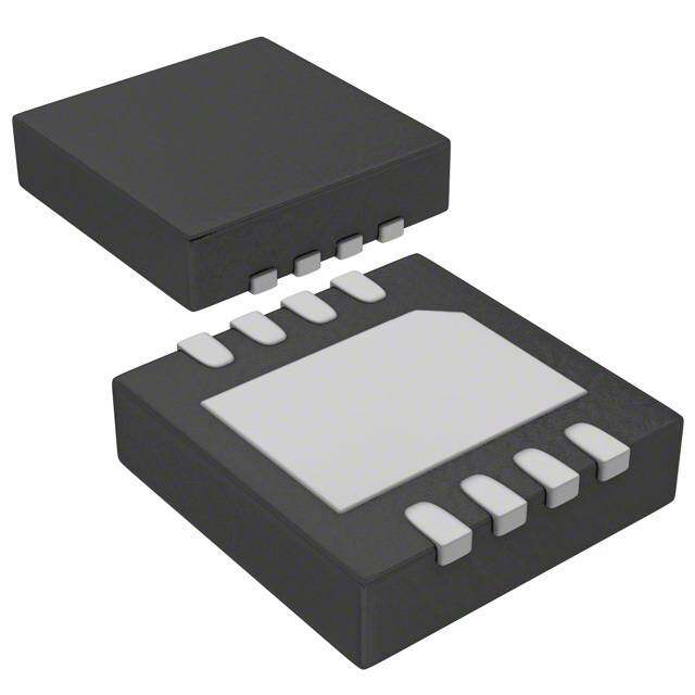
| 产品图片 |
|
| rohs | 符合RoHS无铅 / 符合限制有害物质指令(RoHS)规范要求 |
| 产品系列 | 电源管理 IC,低压差稳压器,Microchip Technology MCP1790-3302E/DB- |
| 数据手册 | http://www.microchip.com/mymicrochip/filehandler.aspx?ddocname=en534539 |
| 产品型号 | MCP1790-3302E/DB |
| PCN组件/产地 | |
| 产品种类 | 低压差稳压器 |
| 供应商器件封装 | SOT-223-3 |
| 包装 | 管件 |
| 商标 | Microchip Technology |
| 回动电压—最大值 | 1.3 V at 70 mA |
| 安装类型 | 表面贴装 |
| 安装风格 | SMD/SMT |
| 封装 | Tube |
| 封装/外壳 | TO-261-4,TO-261AA |
| 封装/箱体 | SOT-223 |
| 工作温度 | -40°C ~ 125°C |
| 工厂包装数量 | 78 |
| 最大工作温度 | + 125 C |
| 最大输入电压 | 30 V |
| 最小工作温度 | - 40 C |
| 最小输入电压 | + 6 V |
| 标准包装 | 78 |
| 电压-跌落(典型值) | 0.7V @ 70mA |
| 电压-输入 | 6 V ~ 30 V |
| 电压-输出 | 3.3V |
| 电压调节准确度 | 2.5 % |
| 电流-输出 | 70mA |
| 电流-限制(最小值) | - |
| 稳压器拓扑 | 正,固定式 |
| 稳压器数 | 1 |
| 线路调整率 | +/- 0.0002 % / V |
| 负载调节 | 0.2 % |
| 输入偏压电流—最大 | 0.07 mA |
| 输出电压 | 3.3 V |
| 输出电流 | 70 mA |
| 输出端数量 | 1 Output |
| 输出类型 | Fixed |


- 商务部:美国ITC正式对集成电路等产品启动337调查
- 曝三星4nm工艺存在良率问题 高通将骁龙8 Gen1或转产台积电
- 太阳诱电将投资9.5亿元在常州建新厂生产MLCC 预计2023年完工
- 英特尔发布欧洲新工厂建设计划 深化IDM 2.0 战略
- 台积电先进制程称霸业界 有大客户加持明年业绩稳了
- 达到5530亿美元!SIA预计今年全球半导体销售额将创下新高
- 英特尔拟将自动驾驶子公司Mobileye上市 估值或超500亿美元
- 三星加码芯片和SET,合并消费电子和移动部门,撤换高东真等 CEO
- 三星电子宣布重大人事变动 还合并消费电子和移动部门
- 海关总署:前11个月进口集成电路产品价值2.52万亿元 增长14.8%


PDF Datasheet 数据手册内容提取
MCP1790/MCP1791 70 mA, High Voltage Regulator Features General Description • 48V (43.5V ±10%) load dump protected for 180ms The MCP1790/MCP1791 regulator provides up to 70mA with a 30second repetition rate (FORD Test Pulse of current. The input operating voltage range is specified G Loaded) from 6.0V to 30V continuous, 48V absolute max, making • Wide steady state supply voltage, 6.0V - 30.0V it ideal for automotive and commercial 12/24VDC systems. • Extended Junction Temperature Range: -40 to +125°C The MCP1790/MCP1791 has a tight tolerance output • Fixed output voltages: 3.0V, 3.3V, 5.0V voltage load regulation of ±0.2% (typical) and a very good line regulation at ±0.0002%/V (typical). The regu- • Low quiescent current: 70µA typical lator output is stable with ceramic, tantalum, and elec- • Low shutdown quiescent current: 10µA typical trolytic capacitors. The MCP1790/MCP1791 regulator • Output Voltage Tolerances of ±2.5% over the incorporates both thermal and short circuit protection. temperature range The MCP1790 is the 3-pin version of the MCP1790/ • Maximum output current of 70mA @ +125°C MCP1791 family. The MCP1791 is the 5-pin version Junction Temperature and incorporates a Shutdown input signal and a Power • Maximum continuous input voltage of 30V Good output signal. • Internal thermal overload protection, +157°C The regulator is specifically designed to operate in the (typical) Junction Temperature automotive environment and will survive +48V (43.5V • Internal short circuit current limit, 120mA (typical) ±10%) load dump transients and double-battery jumps. for +5V option. The device is designed to meet the stringent quiescent • Short Circuit Current Foldback current requirements of the automotive industry. The • Shutdown Input option (MCP1791) device is also designed for the commercial low voltage fire alarm/detector systems which use 24 VDC to sup- • Power Good Output option (MCP1791) ply the required alarms throughout buildings. The low • High PSRR, -90dB@100Hz (typical) ground current, 110µA (typ.), of the CMOS device will • Stable with 1µF to 1000µF Tantalum and provide a power cost savings to the end users over Electrolytic Capacitors similar bipolar devices. Typical buildings using hun- • Stable with 4.7µF to 1000µF Ceramic Capacitors dreds of 24V powered fire and smoke detectors can see substantial savings on energy consumption and Applications wiring gage reduction compared to bipolar regulators. • Low Voltage A/C powered (24VAC) Fire Alarms, The MCP1790 device will be offered in the 3-pin CO Sensors, HVAC Controls DD-PAK, and SOT-223 packages. 2 • Automotive Electronics The MCP1791 device will be offered in the 5-pin • Automotive Accessory Power Adapters DD-PAK, and SOT-223 packages. • Electronic Thermostat Controls The MCP1790/MCP1791 will have a junction tempera- • Microcontroller power ture operating range of -40°C to +125°C. © 2008 Microchip Technology Inc. DS22075A-page 1
MCP1790/MCP1791 Package Types MCP1790 MCP1791 DDPAK-3 SOT-223-3 DDPAK-5 SOT-223-5 4 6 1 2 3 1 2 3 1 2 3 4 5 1 2 3 4 5 Pin Pin 1 VIN 1 SHDN 2 GND (TAB) 2 V IN 3 V OUT 3 GND (TAB) 4 GND (TAB) 4 V OUT 5 PWRGD 6 GND (TAB) DS22075A-page 2 © 2008 Microchip Technology Inc.
MCP1790/MCP1791 TYPICAL APPLICATION PWRGD MCP1791 R 1 On 100kΩ Off SHDN 1 VIN = 6V to 30V VIN VOUT VOUT = 5.0V @ 70mA GND C 1 C 4.7µF 2 1µF Tantalum MCP1790 1 VIN = 8.0V to 16V VIN VOUT VOUT = 3.3V @ 70mA 5Ω C 1 C 1.0µF 2 1.0µF Tantalum GND © 2008 Microchip Technology Inc. DS22075A-page 3
MCP1790/MCP1791 1.0 ELECTRICAL † Notice: Stresses above those listed under “Maximum Rat- ings” may cause permanent damage to the device. This is a CHARACTERISTICS stress rating only and functional operation of the device at those or any other conditions above those indicated in the Absolute Maximum Ratings † operational listings of this specification is not implied. Expo- sure to maximum rating conditions for extended periods may Input Voltage, VIN.........................................................+48.0V affect device reliability. VIN, PWRGD, SHDN.....................(GND-0.3V) to (V +0.3V) IN VOUT..................................................(GND-0.3V) to (+5.5V) Internal Power Dissipation............Internally-Limited (Note4) Output Short Circuit Current..................................Continuous Storage temperature.....................................-55°C to +150°C Maximum Junction Temperature.....................165°C (Note7) Operating Junction Temperature...................-40°C to +125°C ESD protection on all pins..........≥ 6kV HBM and ≥ 400V MM AC/DC CHARACTERISTICS Electrical Specifications: Unless otherwise noted, V = V + V (Note1), I = 1mA, IN OUT(MAX) DROPOUT(MAX), OUT C = 4.7µF (X7R Ceramic), C =4.7µF (X7R Ceramic), T = +25°C, SHDN > 2.4V. OUT IN A Boldface type applies for junction temperatures, T (Note5) of -40°C to +125°C. J Parameters Symbol Min Typ Max Units Conditions Input Operating Voltage V 6.0 — 30.0 V +48V Load Dump Peak IN DC < 500ms Input Quiescent Current I — 70 130 µA I = 0mA q L Input Quiescent Current for SHDN I — 10 25 µA SHDN = GND SHDN Mode Ground Current I — 110 210 µA I = 70mA GND L Maximum Output Current I 70 — — mA OUT Line Regulation ΔV / — ±0.0002 ±0.05 %/V 6.0V < V < 30V OUT IN (V XΔV ) OUT IN Load Regulation ΔV /V -0.45 ±0.2 0.45 % I = 1mA to 70mA OUT OUT OUT (Note3) Output Peak Short Circuit Current I — V /10 — A R <0.1Ω, OUT_SC R LOAD Peak Current Output Voltage Regulation V V -2.5% V V +2.5% V 6.0V < V < 30V OUT R R R IN V Temperature Coefficient TCV — 65 — ppm/°C Note9 OUT OUT Input Voltage to Turn On Output V — 5.5 6.0 V Rising V ON IN Note 1: The minimum V , V must meet two conditions: V ≥ 6.0V and V ≥ V + V IN IN(MIN) IN IN OUT(MAX) DROPOUT(MAX). 2: V is the nominal regulator output voltage. R 3: Load regulation is measured at a constant junction temperature using low duty cycle pulse testing. Load regulation is tested over a load range from 1 mA to the maximum specified output current. 4: The maximum allowable power dissipation is a function of ambient temperature, the maximum allowable junction temperature and the thermal resistance from junction to air. (i.e., T , T , θ ). Exceeding the maximum allowable power A J JA dissipation will cause the device operating junction temperature to exceed the maximum 165°C rating. Sustained junction temperatures above 165°C can impact the device reliability. 5: The junction temperature is approximated by soaking the device under test at an ambient temperature equal to the desired Junction temperature. The test time is small enough such that the rise in the Junction temperature over the ambient temperature is not significant. 6: Dropout voltage is defined as the input-to-output voltage differential at which the output voltage drops 2% below its nominal value that was measured with an input voltage of V = V + V . IN R DROPOUT(MAX) 7: Sustained junction temperatures above 165°C can impact the device reliability. 8: The Short Circuit Recovery Time test is done by placing the device into a short circuit condition and then removing the short circuit condition before the device die temperature reaches 125 °C. If the device goes into thermal shutdown, then the Short Circuit Recovery Time will depend upon the thermal dissipation properties of the package and circuit board. 9: TCV = (V - V ) *10^6 / (V * ΔTemperature), V = highest voltage measured over the tem- OUT OUT-HIGH OUT-LOW R OUT-HIGH peraturerange. V = lowest voltage measured over the temperature range. OUT-LOW DS22075A-page 4 © 2008 Microchip Technology Inc.
MCP1790/MCP1791 AC/DC CHARACTERISTICS (CONTINUED) Electrical Specifications: Unless otherwise noted, V = V + V (Note1), I = 1mA, IN OUT(MAX) DROPOUT(MAX), OUT C = 4.7µF (X7R Ceramic), C =4.7µF (X7R Ceramic), T = +25°C, SHDN > 2.4V. OUT IN A Boldface type applies for junction temperatures, T (Note5) of -40°C to +125°C. J Parameters Symbol Min Typ Max Units Conditions Short Circuit Foldback Voltage Corner V — 4.2 — V V = 5.0V FOLDBACK R Falling V R <0.1Ω OUT, LOAD — 3.0 — V V = 3.3V R Falling V R <0.1Ω OUT, LOAD — 2.7 — V V = 3.0V R Falling V R <0.1Ω OUT, LOAD Short Circuit Foldback Current — 105 — mA V ~= 0V, OUT R <0.1Ω, LOAD V = 5.0V (Note2) R — 99 — mA V = 3.3V (Note2) R — 99 — mA V = 3.0V (Note2) R Startup Voltage Overshoot V — 0.10 — % V V = 0V to 6.0V OVER OUT IN Dropout Voltage V — 700 1300 mV I = 70mA, (Note6) DROPOUT OUT Dropout Current I — 130 — µA V = 5.0V, V = 4.500V DO R IN IOUT = 0 mA — 75 — µA VR = 3.3V, VIN = 4.500V — 75 — µA V = 3.0V, V = 4.500V R IN Shutdown Input Logic High Input V 2.4 — V V SHDN-HIGH IN(MAX) Logic Low Input V 0 — 0.8 V SHDN-LOW Shutdown Input Leakage Current SHDN — 0.100 0.500 µA SHDN = GND ILK — 3.0 5.0 SHDN = 6V Power Good Characteristics PWRGD Input Voltage Operating V 2.8 — — V PWRGD_VIN Range PWRGD Threshold Voltage V 88 90 92 %V Falling Edge of V PWRGD_TH OUT OUT (Referenced to V OUT) PWRGD Threshold Hysteresis V 1.0 2.0 3.0 %V Rising Edge of V PWRGD_HYS OUT OUT PWRGD Output Voltage LOW V — 0.2 0.4 V I = 5.0mA, PWRGD_L PWRGDSINK V = 0V OUT PWRGD Output Sink Current I 5.0 — — mA V <= 0.4V PWRGD_L PWRGD PWRGD Leakage I _ — 1.0 — nA V = V = 6.0V PWRGD LK PWRGD IN PWRGD Time Delay T — 30 — µs Rising Edge PG Note 1: The minimum V , V must meet two conditions: V ≥ 6.0V and V ≥ V + V IN IN(MIN) IN IN OUT(MAX) DROPOUT(MAX). 2: V is the nominal regulator output voltage. R 3: Load regulation is measured at a constant junction temperature using low duty cycle pulse testing. Load regulation is tested over a load range from 1 mA to the maximum specified output current. 4: The maximum allowable power dissipation is a function of ambient temperature, the maximum allowable junction temperature and the thermal resistance from junction to air. (i.e., T , T , θ ). Exceeding the maximum allowable power A J JA dissipation will cause the device operating junction temperature to exceed the maximum 165°C rating. Sustained junction temperatures above 165°C can impact the device reliability. 5: The junction temperature is approximated by soaking the device under test at an ambient temperature equal to the desired Junction temperature. The test time is small enough such that the rise in the Junction temperature over the ambient temperature is not significant. 6: Dropout voltage is defined as the input-to-output voltage differential at which the output voltage drops 2% below its nominal value that was measured with an input voltage of V = V + V . IN R DROPOUT(MAX) 7: Sustained junction temperatures above 165°C can impact the device reliability. 8: The Short Circuit Recovery Time test is done by placing the device into a short circuit condition and then removing the short circuit condition before the device die temperature reaches 125 °C. If the device goes into thermal shutdown, then the Short Circuit Recovery Time will depend upon the thermal dissipation properties of the package and circuit board. 9: TCV = (V - V ) *10^6 / (V * ΔTemperature), V = highest voltage measured over the tem- OUT OUT-HIGH OUT-LOW R OUT-HIGH peraturerange. V = lowest voltage measured over the temperature range. OUT-LOW © 2008 Microchip Technology Inc. DS22075A-page 5
MCP1790/MCP1791 AC/DC CHARACTERISTICS (CONTINUED) Electrical Specifications: Unless otherwise noted, V = V + V (Note1), I = 1mA, IN OUT(MAX) DROPOUT(MAX), OUT C = 4.7µF (X7R Ceramic), C =4.7µF (X7R Ceramic), T = +25°C, SHDN > 2.4V. OUT IN A Boldface type applies for junction temperatures, T (Note5) of -40°C to +125°C. J Parameters Symbol Min Typ Max Units Conditions Detect Threshold to PWRGD Active TV — 235 — µs V = V + DET-PWRG OUT PWRGD_TH Time Delay 100mV to V - D PWRGD_TH 100mV AC Performance Output Delay From SHDN T — 200 — µs SHDN = GND to V OR IN, V = GND to 95% V OUT R, C = 1.0µF OUT PWRGD Delay from SHDN T — 400 — ns SHDN = V to GND SHDN_PG IN , C = 1.0µF OUT Output Noise e — 1.2 — µV/√Hz) I = 50mA, f = 1kHz N OUT Power Supply Ripple Rejection Ratio PSRR dB V = 7.0V, C = 0µF, IN IN I = 10mA, OUT V = 400mVpp INAC — 90 — f = 100Hz — 75 — f = 1kHz, V = 5.0V R — 80 — f = 1kHz, V = < 5.0V R Thermal Shutdown Temperature T — 157 — °C Rising Temperature SD Thermal Shutdown Hysteresis ΔT — 20 — °C Falling Temperature SD Short Circuit Recovery Time t — 0 — ms (Note8) THERM Note 1: The minimum V , V must meet two conditions: V ≥ 6.0V and V ≥ V + V IN IN(MIN) IN IN OUT(MAX) DROPOUT(MAX). 2: V is the nominal regulator output voltage. R 3: Load regulation is measured at a constant junction temperature using low duty cycle pulse testing. Load regulation is tested over a load range from 1 mA to the maximum specified output current. 4: The maximum allowable power dissipation is a function of ambient temperature, the maximum allowable junction temperature and the thermal resistance from junction to air. (i.e., T , T , θ ). Exceeding the maximum allowable power A J JA dissipation will cause the device operating junction temperature to exceed the maximum 165°C rating. Sustained junction temperatures above 165°C can impact the device reliability. 5: The junction temperature is approximated by soaking the device under test at an ambient temperature equal to the desired Junction temperature. The test time is small enough such that the rise in the Junction temperature over the ambient temperature is not significant. 6: Dropout voltage is defined as the input-to-output voltage differential at which the output voltage drops 2% below its nominal value that was measured with an input voltage of V = V + V . IN R DROPOUT(MAX) 7: Sustained junction temperatures above 165°C can impact the device reliability. 8: The Short Circuit Recovery Time test is done by placing the device into a short circuit condition and then removing the short circuit condition before the device die temperature reaches 125 °C. If the device goes into thermal shutdown, then the Short Circuit Recovery Time will depend upon the thermal dissipation properties of the package and circuit board. 9: TCV = (V - V ) *10^6 / (V * ΔTemperature), V = highest voltage measured over the tem- OUT OUT-HIGH OUT-LOW R OUT-HIGH peraturerange. V = lowest voltage measured over the temperature range. OUT-LOW DS22075A-page 6 © 2008 Microchip Technology Inc.
MCP1790/MCP1791 TEMPERATURE SPECIFICATIONS Parameters Symbol Min Typ Max Units Conditions Temperature Ranges Specified Temperature Range T -40 +125 °C J Operating Temperature Range T -40 +125 °C J Storage Temperature Range T -55 +150 °C J Package Thermal Resistances Thermal Resistance, 3LD DDPAK θ — 31.4 — °C/W EIA/JEDEC JESD51-751-7 JA θ 3 4 Layer Board JC Thermal Resistance, 3LD SOT-223 θ — 62 — °C/W EIA/JEDEC JESD51-751-7 JA θ 15 4 Layer Board JC Thermal Resistance, 5LD DDPAK θ — 31.4 — °C/W EIA/JEDEC JESD51-751-7 JA θ 3 4 Layer Board JC Thermal Resistance, 5LD SOT-223 θ — 62 — °C/W EIA/JEDEC JESD51-751-7 JA θ 15 4 Layer Board JC © 2008 Microchip Technology Inc. DS22075A-page 7
MCP1790/MCP1791 2.0 TYPICAL PERFORMANCE CHARACTERISTICS Note: The graphs and tables provided following this note are a statistical summary based on a limited number of samples and are provided for informational purposes only. The performance characteristics listed herein are not tested or guaranteed. In some graphs or tables, the data presented may be outside the specified operating range (e.g., outside specified power supply range) and therefore outside the warranted range. Note: Unless otherwise indicated, C = 4.7uF Ceramic (X7R), C = 10.0µF Ceramic (X7R), I = 1mA, Temperature = +25°C, OUT IN OUT V = 6.0V, R = 10kΩ To V , V = V and device is MCP1790. IN PWRGD_PULLUP OUT SHDN IN, Note: Junction Temperature (TJ) is approximated by soaking the device under test to an ambient temperature equal to the desired junction temperature. The test time is small enough such that the rise in Junction Temperature over the Ambient temperature is not significant. 50 120.00 µs) 40 VIOOUUTT = = 0 5 µ.0AV µA)100.00 VIOIUNT = = 6 0VµA VOUT = 3.0V e Delay ( 30 VIN = 6V VIN = 10V,15V,25V,30V Current ( 6800..0000 VOUT = 3.3V Tim 20 ent 40.00 VOUT = 5.0V D sc G 10 e R ui 20.00 W Q P 0 0.00 -45 -20 5 30 55 80 105 130 -45 -20 5 30 55 80 105 130 Temperature (°C) Junction Temperature (°C) FIGURE 2-1: Power Good Time Delay vs. FIGURE 2-4: Quiescent Current vs. Temperature (MCP1791). Junction Temperature. 140 140 urrent (µA)11028000 +++1293500°°°CCC VIOOUUTT = = 0 3 µ.3AV ent (µA)11028000 VOVUOTU =T =5 .30.V3V VOUT = 3.0V nt C 60 -450°°CC Curr 60 sce 40 ND 40 e G ui 20 20 Q 0 0 0 5 10 15 20 25 30 35 0 10 20 30 40 50 60 70 Input Voltage (V) Load Current (mA) FIGURE 2-2: Quiescent Current vs. Input FIGURE 2-5: Ground Current vs. Load Voltage. Current. 140 28 µA)120 VIOOUUTT = = 0 5 µ.0AV 24 VVRSHEGDN = = 3 0.0VV nt (100 +130°C 20 cent Curre 468000 ++-2945005°°°°CCCC I (µA)SHDN11268 VIN = 10V, 30V s uie 20 4 VIN = 6.0V Q 0 0 0 5 10 15 20 25 30 35 -45 -20 5 30 55 80 105 130 Input Voltage (V) Temperature (°C) FIGURE 2-3: Quiescent Current vs. Input FIGURE 2-6: I vs Temperature. SHDN Voltage. DS22075A-page 8 © 2008 Microchip Technology Inc.
MCP1790/MCP1791 Note: Unless otherwise indicated, C = 4.7uF Ceramic (X7R), C = 10.0µF Ceramic (X7R), I = 1mA, Temperature = +25°C, OUT IN OUT V = 6.0V, R = 10kΩ To V , V = V and device is MCP1790. IN PWRGD_PULLUP OUT SHDN IN, 0.006 5.04 VOUT = 3.3V 5.03 VOUT = 5.0V %/V) 00..000024 10 mA 0 mA VIN = 6V to 30V e (V) 55..0012 VIN = 6.3V n ( ag 5.00 atio 0.000 Volt 4.99 gul -0.002 ut 4.98 e Re -0.004 70 mA Outp 44..9967 Lin 4.95 --4455°°CC 00°°CC ++2255°°CC ++9900°°CC ++113300°°CC -0.006 4.94 -45 -20 5 30 55 80 105 130 0 10 20 30 40 50 60 70 Temperature (°C) Load Current (mA) FIGURE 2-7: Line Regulation vs. FIGURE 2-10: Output Voltage vs. Load Temperature. Current. 0.006 1.0 VOUT = 5.0V 0.9 VOUT = 5.0V V) 0.004 VIN = 6V to 30V V)0.8 ation (%/ 00..000002 0 mA Voltage (000...567 +90°C+130°C Line Regul --00..000042 30 mA 70 mA Dropout 0000....1234 -45°C 0°C +25°C -0.006 0.0 -45 -20 5 30 55 80 105 130 0 10 20 30 40 50 60 70 Temperature (°C) Load Current (mA) FIGURE 2-8: Line Regulation vs. FIGURE 2-11: Dropout Voltage vs. Load Temperature. Current. 0.00 1.0 ILOAD = 1 mA to 70 mA 0.9 VOUT = 5.0V n (%) --00..1005 VREG=5.0V age (V)000...678 70 mA ad Regulatio ---000...221505 VREG=3.0VVREG=3.3V Dropout Volt0000....2345 513000 mmmAAA 1 mA o 0.1 L -0.30 0.0 -45 -20 5 30 55 80 105 130 -45 -20 5 30 55 80 105 130 Temperature (°C) Temperature (°C) FIGURE 2-9: Load Regulation vs. FIGURE 2-12: Dropout Voltage vs. Temperature. Temperature. © 2008 Microchip Technology Inc. DS22075A-page 9
MCP1790/MCP1791 Note: Unless otherwise indicated, C = 4.7uF Ceramic (X7R), C = 10.0µF Ceramic (X7R), I = 1mA, Temperature = +25°C, OUT IN OUT V = 6.0V, R = 10kΩ To V , V = V and device is MCP1790. IN PWRGD_PULLUP OUT SHDN IN, 130 -20 mA)125 ROUT < 0.1Ω -30 VR=5.0V Circuit Current (111112050 VOUT = 5.0V VOUT = 3.3V PSRR (dB) ------987654000000 VVCIOIIIUNNNT=A==C701 . =0μ0 V 4Fm00A mV p-p ort 105 VOUT = 3.0V -100 h S100 -110 -120 6 10 14 18 22 26 30 0.01 0.1 1 10 100 1000 Input Voltage (V) Frequency (kHz) FIGURE 2-13: Short Circuit Current vs FIGURE 2-16: Power Supply Ripple Input Voltage. Rejection vs. Frequency. 10.00 VR=5.0V IOUT=50mA 1.00 z) H(cid:165) VR=3.3V V/ μ 0.10 e ( s oi N 0.01 0.00 0.01 0.1 1 10 100 1000 Frequency (kHz) FIGURE 2-14: Output Noise Voltage FIGURE 2-17: Startup from V IN Density vs. Frequency. (MCP1791). -20 -30 VR=3.3V VIN=7.0V -40 VINAC = 400 mV p-p dB) --6500 CIOIUNT==01 μ0 FmA R ( R -70 S P -80 -90 -100 -110 0.01 0.1 1 10 100 1000 Frequency (kHz) FIGURE 2-15: Power Supply Ripple FIGURE 2-18: Startup from Shutdown Rejection vs. Frequency. (MCP1791). DS22075A-page 10 © 2008 Microchip Technology Inc.
MCP1790/MCP1791 Note: Unless otherwise indicated, C = 4.7uF Ceramic (X7R), C = 10.0µF Ceramic (X7R), I = 1mA, Temperature = +25°C, OUT IN OUT V = 6.0V, R = 10kΩ To V , V = V and device is MCP1790. IN PWRGD_PULLUP OUT SHDN IN, FIGURE 2-19: Dynamic Line Response. FIGURE 2-22: Dynamic Load Response. 5.0 4.5 V)4.0 VOUT = 3.3V e (3.5 ag3.0 olt2.5 ut V2.0 VOUT = 3.0V p1.5 Out1.0 0.5 0.0 0 20 40 60 80 100 120 140 Output Current (mA) FIGURE 2-20: Dynamic Line Response. FIGURE 2-23: Short Circuit Response. 7 VOUT = 5.0V V)6 VIN = 6.3V e (5 g a4 olt V3 ut utp2 O 1 0 0 20 40 60 80 100 120 140 Output Current (mA) FIGURE 2-21: Dynamic Load Response. FIGURE 2-24: Short Circuit Response. © 2008 Microchip Technology Inc. DS22075A-page 11
MCP1790/MCP1791 Note: Unless otherwise indicated, C = 4.7uF Ceramic (X7R), C = 10.0µF Ceramic (X7R), I = 1mA, Temperature = +25°C, OUT IN OUT V = 6.0V, R = 10kΩ To V , V = V and device is MCP1790. IN PWRGD_PULLUP OUT SHDN IN, 90 µA)80 IOUT = 1 mA nt (70 e Curr5600 VOUT = 5.0V d un40 VOUT = 3.3V Gro30 p 20 u art10 St 0 0 1 2 3 4 5 6 7 Input Voltage (V) FIGURE 2-25: Startup Ground Current. DS22075A-page 12 © 2008 Microchip Technology Inc.
MCP1790/MCP1791 3.0 PIN DESCRIPTIONS The descriptions of the pins are listed in Table3-1 and Table3-2. TABLE 3-1: MCP1790 PIN FUNCTION TABLE Pin No. Pin No. Symbol Function SOT-223-3 DDPAK-3 1 1 V Unregulated Supply Voltage IN 2,Tab 2,Tab GND Ground Terminal 3 3 V Regulated Output Voltage OUT TABLE 3-2: MCP1791 PIN FUNCTION TABLE Pin No. Pin No. Symbol Function SOT-223-5 DDPAK-5 1 1 SHDN Shutdown Input 2 2 V Unregulated Supply Voltage IN 3 3 GND Ground Terminal 4 4 V Regulated Output Voltage OUT 5 5 PWRGD Power Good Open-Drain Output Tab Tab — Connected to Ground — — N/C no connection 3.1 Input Voltage Supply (V ) 3.4 Shutdown (SHDN) IN Connect the unregulated or regulated input voltage The SHDN pin is an active-low input signal that turns source to V . If the input voltage source is located sev- the regulator output voltage on and off. When the IN eral inches away from the regulator or the input source SHDN input is at a logic-high level, the regulator output is a battery, it is recommended that an input capacitor voltage is enabled. When the SHDN input is pulled to a is used. A typical input capacitance value of 1µF to logic-low level, the regulator output voltage is disabled. 10µF should be sufficient for most applications. The When the SHDN input is pulled low, the PWRGD output type of capacitor used can be ceramic, tantalum or alu- signal also goes low and the regulator enters a low qui- minum electrolytic. The low ESR characteristics of the escent current shutdown state where the typical quies- ceramic will yield better noise and PSRR performance cent current is 10µA. The SHDN pin is bonded to V IN at high-frequency. in the 3-pin versions of the regulator. See Table4-1. 3.2 Ground (GND) 3.5 Power Good Output (PWRGD) Tie GND to the negative side of the output and the The PWRGD pin is an open-drain output signal that is negative side of the input capacitor. Only the regulator used to indicate when the regulator output voltage is bias current flows out of this pin; there is no high within 90% (typically) of its nominal regulation value. current. The regulator output regulation is referenced to The PWRGD threshold has a typical hysteresis value this pin. Minimize voltage drops between this pin and of 2%. The typical PWRGD delay time due to V OUT the negative side of the load. rising above 90% +3% (maximum hysteresis) is 30µs. The typical PWRGD delay time due to V falling OUT 3.3 Regulated Output Voltage (V ) below 90% is 235µs. These delay times are internally OUT fixed. The V pin is the regulated output voltage of the reg- OUT ulator. A minimum output capacitance of 1.0µF tanta- 3.6 Exposed Pad (EP) lum, 1.0 µF electrolytic, or 4.7µF ceramic is required for stability. The MCP1790 is stable with ceramic, The DDPAK package has an exposed tab on the pack- tantalum, and electrolytic capacitors. See Section4.7 age. A heat sink may be mounted to the tab to aid in the “Output Capacitor” for output capacitor selection removal of heat from the package during operation. guidance. The exposed tab or pad of all of the available packages is at the ground potential of the regulator. © 2008 Microchip Technology Inc. DS22075A-page 13
MCP1790/MCP1791 4.0 DEVICE OVERVIEW 4.4 External Protection The MCP1790/MCP1791 are high input voltage regula- 4.4.1 TRANSIENT VOLTAGE tors capable of providing up to 70mA of current at PROTECTION (LOAD DUMP) output voltages up to 5.0V. The devices have an input voltage operating range from 6.0V to 30V, 48V absolute The regulator is capable of withstanding a 48V max. The MCP1790 devices are 3-pin devices consist- (43.5V±10) load dump transient for a duration of ing of V , V , and GND. The MCP1791 devices 180ms and a repetition rate of 30 seconds IN OUT have 5 or more pins which add Shutdown and (ES-XW7T-1A278-AC, Ford Motor Company, Test Power-Good functions to the MCP1790 device. Pulse G Loaded). While not necessary, good design practice dictates 4.1 Startup adding an external transient suppressor, between VBB and ground, with a low value resistor in series with the In the start phase, the device must see at least 6.0V to battery supply and the VIN pin, to limit currents and initiate operation during power up. In the Power-down voltages due to electrical transients. Because of the mode, the V monitor will be turned off. IN regulator startup current, the resistor value should be less than (V -6V)/200mA. For a 12V battery volt- BAT 4.2 Thermal Shutdown age, the resistor value should be less than 30 ohms. The regulator has a thermal shutdown. If the thermal 4.4.2 REVERSE BATTERY PROTECTION protection circuit detects an over temperature condition, typically 157°C junction temperature, the An external reverse battery blocking diode may be regulator will shut down. The device will recover from used to provide polarity protection. the thermal shutdown when the junction temperature drops to 137°C (typical). 4.3 Regulator Output Voltage The MCP1790/MCP1791 regulators are available in fixed output voltage configurations. The standard output voltages are 3.0V, 3.3V, and 5.0V. VIN T1 T2 Soft Start e - onitoringmperatur RVefoeltraegnece en Error Amplifier T1 MTe T2 Temp + Sensor Short Circuit VOUT Logical Block Protection en 510k VIN 490k Delay SHDN Monitoring VOUT Delay PWRGD Monitoring VIN GND FIGURE 4-1: MCP1790/MCP1791 Block Diagram. DS22075A-page 14 © 2008 Microchip Technology Inc.
MCP1790/MCP1791 4.5 Shutdown (SHDN) 4.6 Low Voltage Shutdown The MCP1791 has a Shutdown (SHDN) input signal The MCP1790/MCP1791 incorporates a Low Voltage that enables or disables the regulator output voltage. Shutdown circuit that turns off the output of the regula- When the SHDN input signal is greater than 2.40V, the tor whenever the input voltage, V , is below the IN regulator output voltage is enabled. Note that the specified turn off voltage, V . When the input voltage OFF regulator output may still be disabled by the undervolt- (V ) drops below the differential needed to provide B age lockout incorporated within the V circuitry. stable regulation, the output voltage (V ) shall track IN REG the input down to approximately +4.00V. The regulator The value of the SHDN signal to put the regulator into will turn off the output at this point. Shutdown mode is ≤ 0.8V. The SHDN pin is pulled low by an internal resistor. If the SHDN pin is left floating, The output will turn on when V rises above the V IN ON the internal pull-down resistor will put the regulator into value specified in the data sheet. This feature is shutdown mode. independent of the Shutdown input signal (SHDN) that is provided for external regulator control. If the SHDN When the SHDN input signal is pulled to a logic-low, the input signal is active (LOW), then the output of the PWRGD output signal will also go low and the regulator regulator shall be disabled regardless of input voltage. will enter a low quiescent current state where the typi- cal quiescent current is 10µA. There is a short time TABLE 4-1: SHUTDOWN LOGIC delay (approximately 400ns) when the SHDN input signal transitions from high to low to prevent signal V SHDN V IN OUT noise from disabling the regulator. The SHDN pin will ignore low-going pulses that are up to 400ns in pulse < VOFF L OFF width. If the SHDN input is pulled low for more than < V H OFF OFF 400ns, the regulator will enter Shutdown mode. This > V L OFF ON small bit of filtering helps to reject any system noise > V H ON spikes on the SHDN input signal. ON On the rising edge of the SHDN input, the shutdown 4.7 Output Capacitor circuitry will have a 100µs delay before allowing the regulator output to turn on. This delay helps to reject The MCP1790/MCP1791 requires a minimum output any false turn-on signals or noise on the SHDN input capacitance of 1µF tantalum or electrolytic capaci- signal. After the 100µs delay, the regulator will start tance. The minimum value for ceramic capacitors is charging the output capacitor as the regulator output 4.7µF. The regulator is stable for all three types of voltage rises from 0V to its final regulated value. The capacitors from 4.7µF to 1000µF (see Figure4-3). charging current will be limited by the short circuit The MCP1790/MCP1791 regulator may be used with a current value of the device. If the SHDN input signal is 1µF ceramic output capacitor if a 0.300Ω resistor is pulled low during the 100µs delay period, the timer will placed in series with the capacitor. The low ESR and be reset and the delay time will start over again on the corresponding pole of the ceramic capacitor causes the next rising edge of the SHDN input. The total time from instability below 4.7µF. the SHDN input going high (turn-on) to the regulator The Equivalent Series Resistance (ESR) of the output output being in regulation shall typically be 200µs capacitor must be no greater than 3 ohms. The output (100µs + 100µs) for a C = 1.0µF. LOAD capacitor should be located as close to the regulator output as is practical. Ceramic materials X7R and X5R TOR CLOAD CHARGING TIME have low temperature coefficients and are recommended because of their size, cost, and 400ns (typ) environmental robustness qualities. 100µs 100µs SHDN VOUT C = 1.0µF LOAD FIGURE 4-2: Shutdown Input Timing Diagram. © 2008 Microchip Technology Inc. DS22075A-page 15
MCP1790/MCP1791 4.8 Output Current and Current The 5.0V regulator has an overload current limiting of Limiting approximately 120mA. If VREG is lower than 3.5V, IOUT will start to fold back and decrease along with V REG The MCP1790/MCP1791 devices are tested and until I is less than 105mA and V is near 0 volts. OUT REG ensured to supply a minimum of 70mA of output The 3.3V regulator has an overload current limiting of current. approximately 130mA. If V is lower than 2.5V, I REG OUT The MCP1790/MCP1791 also incorporate an output will start to fold back and decrease along with V REG current limit foldback. When the regulator is in an until I is less than 99mA and V is near 0 volts. OUT REG overcurrent condition, V will decrease with increas- OUT ing load. When V falls below 30% (typical) of V , OUT R the output current will start to fold back. The output current will fold back to less than 100mA (typical) when V is near 0 volts. OUT ESR Curves 10 Instable Stable only 1 with Tantalum or Electrolytic cap. Stable ] with m Tantalum, h Electrolytic and o Instable Ceramic cap. [ 0.1 R S E 0.01 Instable 0.001 0.1 1 10 100 1000 Load Capacitor [uF] FIGURE 4-3: ESR Curves For Load Capacitor Selection. DS22075A-page 16 © 2008 Microchip Technology Inc.
MCP1790/MCP1791 4.9 Power Good Output (PWRGD) The MCP1791 has an open-drain Power Good (PWRGD) output signal capable of sinking a minimum VPWRGD_TH of 5.0mA of current while maintaining a PWRGD output voltage of 0.4V or less. VOUT VPWRGD_HYS TPG As the output voltage of the LDO rises, the PWRGD output will be held low until the output voltage has 30µs exceeded the power good threshold (V ) level VOH by an amount equal to the power good PhWysRtGerDe_sTiHs value TVDET_PWRGD ((V ), typically 2% of V . Once this threshold 235µs PWRGD_HYS R has been exceeded, the power good output signal will PWRGD be pulled high by an external pull-up resistor, indicating that the output voltage is stable and within regulation VOL limits. If the output voltage of the LDO falls below the power FIGURE 4-4: Power Good Timing. good threshold (V ) level, the power good PWRGD_TH output will transition low. The power good circuitry has a 235µs delay when detecting a falling output voltage, C = 1.0µF LOAD which helps to increase noise immunity of the power good output and avoid false triggering of the power good output during fast output transients. See VIN Figure4-4 for power good timing characteristics. TOR When the LDO is put into Shutdown mode using the 100µs 100µs SHDN input, the power good output is pulled low within 400ns typical, indicating that the output voltage will be out of regulation. The timing diagram for the power SHDN TPG good output when using the shutdown input is shown in Figure4-5. The PWRGD output may be pulled up to either V or IN V . When pulled to V , the PWRGD output will OUT OUT VOUT sink very little current during shutdown. When PWRGD is pulled up to V , the PWRGD output will sink current IN during shutdown. That is because V is 0 during OUT shutdown while V is still active. When the PWRGD IN output is pulled to V , the PWRGD output signal will PWRGD IN track V at startup until the threshold of the PWRGD IN circuitry has been reached and the PWRGD circuitry pulls the signal back low. Therefore, when pulling FIGURE 4-5: Power Good Timing from PWRGD to VIN instead of V , the designer must be Shutdown. OUT aware of the PWRGD signal going high while the input voltage is rising at startup. Pulling PWRGD to V OUT removes the startup pulse. © 2008 Microchip Technology Inc. DS22075A-page 17
MCP1790/MCP1791 5.0 APPLICATION CIRCUITS / EQUATION 5-2: ISSUES T = P ×Rθ +T J(MAX) TOTAL JA AMAX 5.1 Typical Application T = Maximum continuous junction J(MAX) temperature. The MCP1790/MCP1791 is most commonly used as a voltage regulator. It’s high voltage input capability and PTOTAL = Total device power dissipation. thermal protection make it ideal for automotive and 24V Rθ = Thermal resistance from junction JA industrial applications. to ambient. T = Maximum ambient temperature. AMAX The maximum power dissipation capability for a MCP1791 package can be calculated given the junction-to- ambient thermal resistance and the maximum ambient 1 2 3 4 5 PWRGD temperature for the application. The following equation VIN 5 1N4002 10kΩ VOUT can be used to determine the package maximum + + internal power dissipation. 24VDC 1CµINF COUT 5V@70mA 4.7µF Ceramic Ceramic EQUATION 5-3: (T –T ) FIGURE 5-1: Typical Application. P = ------J---(--M----A---X---)------------A---(--M----A---X---)--- D(MAX) Rθ JA 5.1.1 APPLICATION INPUT CONDITIONS PD(MAX) = Maximum device power dissipation. Package Type = SOT-223-5 T = Maximum continuous junction J(MAX) Input Voltage Range = 8V to 24V temperature. VIN maximum = 24V TA(MAX) = Maximum ambient temperature. VOUT typical = 5.0V RθJA = Thermal resistance from junction I = 70mA maximum to ambient. OUT 5.2 Power Calculations EQUATION 5-4: 5.2.1 POWER DISSIPATION T = P ×Rθ J(RISE) D(MAX) JA The internal power dissipation of the MCP1790/ T = Rise in device junction MCP1791 is a function of input voltage, output voltage J(RISE) temperature over the ambient and output current. The power dissipation, as a result temperature. of the quiescent current draw, is so low, it is insignifi- cant (70.0µA x V ). The following equation can be P = Maximum device power IN TOTAL used to calculate the internal power dissipation of the dissipation. LDO. Rθ = Thermal resistance from JA junction-to-ambient. EQUATION 5-1: P = (V –V )×I LDO IN(MAX)) OUT(MIN) OUT(MAX)) EQUATION 5-5: P = LDO Pass device internal power LDO T = T +T dissipation J J(RISE) A V = Maximum input voltage T = Junction Temperature. IN(MAX) J V = LDO minimum output voltage T = Rise in device junction OUT(MIN) J(RISE) temperature over the ambient temperature. The maximum continuous operating junction temperature specified for the MCP1790/MCP1791 is T = Ambient temperature. A +125°C. To estimate the internal junction temperature of the MCP1790/MCP1791, the total internal power dissipation is multiplied by the thermal resistance from junction to ambient (Rθ ). The thermal resistance from JA junction to ambient for the SOT-223-5 package is estimated at 62°C/W. DS22075A-page 18 © 2008 Microchip Technology Inc.
MCP1790/MCP1791 5.3 Power Dissipation Example 5.3.1.2 Junction Temperature Estimate Internal power dissipation, junction temperature rise, To estimate the internal junction temperature, the junction temperature and maximum power dissipation calculated temperature rise is added to the ambient or are calculated in the following example. The power offset temperature. For this example, the worst-case dissipation, as a result of ground current, is small junction temperature is estimated below. enough to be neglected. T = T + T J JRISE A(MAX) 5.3.1 POWER DISSIPATION EXAMPLE T = 99.2°C J Package: 5.3.1.3 Maximum Package Power Package Type = SOT-223-5 Dissipation at +40°C Ambient Input Voltage: Temperature VIN = 8V to 24V SOT-223-5 (62°C/Watt = RθJA) LDO Output Voltages and Currents: P = (125°C - 40°C) / 62°C/W D(MAX) VOUT = 5.0V PD(MAX) = 1.371 Watts IOUT = 50mA DDPAK-5 (32°C/Watt = RθJA) Maximum Ambient Temperature: P = (125°C - 40°C) / 32°C/W D(MAX) TA(MAX) = +40°C PD(MAX) = 2.656 Watts Internal Power Dissipation: Internal Power dissipation is the product of the LDO 5.4 Pulsed Load Applications output current times the voltage across the LDO For some applications, there are pulsed load current (V to V ). IN OUT events that may exceed the specified 70mA maximum P = (V - V ) x I LDO(MAX) IN(MAX) OUT(MIN) OUT(MAX) specification of the MCP1790/MCP1791. The internal PLDO = (24V - (0.98 x 5.0V)) x 50mA current foldback feature of the MCP1790/MCP1791 will P = 955 milli-Watts prevent high peak load demands from causing LDO non-recoverable damage. The Current Foldback 5.3.1.1 Device Junction Temperature Rise feature of the device will limit the output voltage and output current during pulsed applications. As the cur- The internal junction temperature rise is a function of rent rises above the foldback current threshold, the out- internal power dissipation and the thermal resistance put voltage will decrease. from junction to ambient for the application. The thermal resistance from junction to ambient (Rθ ) is JA derived from an EIA/JEDEC standard for measuring thermal resistance for small surface mount packages. The EIA/JEDEC specification is JESD51-7, “High Effective Thermal Conductivity Test Board for Leaded Surface Mount Packages”. The standard describes the test method and board specifications for measuring the thermal resistance from junction to ambient. The actual thermal resistance for a particular application can vary depending on many factors, such as copper area and thickness. Refer to AN792, “A Method to Determine How Much Power a SOT23 Can Dissipate in an Application”, (DS00792), for more information regarding this subject. T = P x Rq J(RISE) TOTAL JA TJRISE = 955 milli-Watts x 62°C/Watt TJRISE = 59.2°C © 2008 Microchip Technology Inc. DS22075A-page 19
MCP1790/MCP1791 6.0 PACKAGING INFORMATION 6.1 Package Marking Information 3-Lead DDPAK (MCP1790) Example: XXXXXXXXX MCP1790 XXXXXXXXX 50EEB^e^3 YYWWNNN 0730256 1 2 3 1 2 3 3-Lead SOT-223 (MCP1790) Example: XXXXXXX 179050 XXXYYWW EDB0730 NNN 256 Legend: XX...X Customer-specific information Y Year code (last digit of calendar year) YY Year code (last 2 digits of calendar year) WW Week code (week of January 1 is week ‘01’) NNN Alphanumeric traceability code e3 Pb-free JEDEC designator for Matte Tin (Sn) * This package is Pb-free. The Pb-free JEDEC designator ( e 3 ) can be found on the outer packaging for this package. Note: In the event the full Microchip part number cannot be marked on one line, it will be carried over to the next line, thus limiting the number of available characters for customer-specific information. DS22075A-page 20 © 2008 Microchip Technology Inc.
MCP1790/MCP1791 6.1 Package Marking Information (Continued) 5-Lead DDPAK (Fixed) (MCP1791) Example: XXXXXXXXX MCP1791 XXXXXXXXX 50EET^e^3 YYWWNNN 0730256 1 2 3 4 5 1 2 3 4 5 5-Lead SOT-223 (MCP1791) Example: XXXXXXX 179150 XXXYYWW EDC0730 NNN 256 Legend: XX...X Customer-specific information Y Year code (last digit of calendar year) YY Year code (last 2 digits of calendar year) WW Week code (week of January 1 is week ‘01’) NNN Alphanumeric traceability code e3 Pb-free JEDEC designator for Matte Tin (Sn) * This package is Pb-free. The Pb-free JEDEC designator ( e 3 ) can be found on the outer packaging for this package. Note: In the event the full Microchip part number cannot be marked on one line, it will be carried over to the next line, thus limiting the number of available characters for customer-specific information. © 2008 Microchip Technology Inc. DS22075A-page 21
MCP1790/MCP1791 (cid:2)(cid:3)(cid:4)(cid:5)(cid:6)(cid:7)(cid:8)(cid:9)(cid:10)(cid:6)(cid:11)(cid:12)(cid:13)(cid:14)(cid:8)(cid:15)(cid:16)(cid:17)(cid:18)(cid:8)(cid:19)(cid:20)(cid:20)(cid:9)(cid:21)(cid:22)(cid:23) (cid:24)(cid:25)(cid:12)(cid:5)(cid:26) +(cid:22)(cid:16)(cid:5)(cid:13)(cid:15)(cid:17)(cid:5)(cid:21)(cid:22)(cid:18)(cid:13)(cid:5)(cid:11)(cid:26)(cid:16)(cid:16)(cid:17)(cid:9)(cid:13)(cid:5)(cid:27)(cid:12)(cid:11),(cid:12)(cid:8)(cid:17)(cid:5)(cid:23)(cid:16)(cid:12)*(cid:7)(cid:9)(cid:8)(cid:18)-(cid:5)(cid:27)(cid:25)(cid:17)(cid:12)(cid:18)(cid:17)(cid:5)(cid:18)(cid:17)(cid:17)(cid:5)(cid:13)(cid:15)(cid:17)(cid:5)(cid:28)(cid:7)(cid:11)(cid:16)(cid:22)(cid:11)(cid:15)(cid:7)(cid:27)(cid:5).(cid:12)(cid:11),(cid:12)(cid:8)(cid:7)(cid:9)(cid:8)(cid:5)(cid:6)(cid:27)(cid:17)(cid:11)(cid:7)(cid:10)(cid:7)(cid:11)(cid:12)(cid:13)(cid:7)(cid:22)(cid:9)(cid:5)(cid:25)(cid:22)(cid:11)(cid:12)(cid:13)(cid:17)(cid:23)(cid:5)(cid:12)(cid:13)(cid:5) (cid:15)(cid:13)(cid:13)(cid:27)&//***(cid:3)(cid:21)(cid:7)(cid:11)(cid:16)(cid:22)(cid:11)(cid:15)(cid:7)(cid:27)(cid:3)(cid:11)(cid:22)(cid:21)/(cid:27)(cid:12)(cid:11),(cid:12)(cid:8)(cid:7)(cid:9)(cid:8) E E1 L1 D1 D H 1 N b e BOTTOMVIEW TOPVIEW b1 CHAMFER OPTIONAL A C2 φ A1 c L 0(cid:9)(cid:7)(cid:13)(cid:18) 12(cid:14)3(cid:24)(cid:6) (cid:20)(cid:7)(cid:21)(cid:17)(cid:9)(cid:18)(cid:7)(cid:22)(cid:9)(cid:5)4(cid:7)(cid:21)(cid:7)(cid:13)(cid:18) (cid:28)12 25(cid:28) (cid:28)"6 2(cid:26)(cid:21)7(cid:17)(cid:16)(cid:5)(cid:22)(cid:10)(cid:5).(cid:7)(cid:9)(cid:18) 2 ! .(cid:7)(cid:13)(cid:11)(cid:15) (cid:17) (cid:3)(cid:2)(cid:30)(cid:30)(cid:5)%(cid:6)(cid:14) 5)(cid:17)(cid:16)(cid:12)(cid:25)(cid:25)(cid:5)3(cid:17)(cid:7)(cid:8)(cid:15)(cid:13) " (cid:3)(cid:2)8(cid:30) 9 (cid:3)(cid:2):(cid:30) (cid:6)(cid:13)(cid:12)(cid:9)(cid:23)(cid:22)(cid:10)(cid:10)(cid:5)(cid:5)(cid:4) "(cid:2) (cid:3)(cid:30)(cid:30)(cid:30) 9 (cid:3)(cid:30)(cid:2)(cid:30) 5)(cid:17)(cid:16)(cid:12)(cid:25)(cid:25)(cid:5);(cid:7)(cid:23)(cid:13)(cid:15) (cid:24) (cid:3)!<(cid:30) 9 (cid:3)$(cid:19)(cid:30) (cid:24)(cid:29)(cid:27)(cid:22)(cid:18)(cid:17)(cid:23)(cid:5).(cid:12)(cid:23)(cid:5);(cid:7)(cid:23)(cid:13)(cid:15) (cid:24)(cid:2) (cid:3)(cid:19)$(cid:31) 9 9 (cid:28)(cid:22)(cid:25)(cid:23)(cid:17)(cid:23)(cid:5).(cid:12)(cid:11),(cid:12)(cid:8)(cid:17)(cid:5)4(cid:17)(cid:9)(cid:8)(cid:13)(cid:15) (cid:20) (cid:3)!!(cid:30) 9 (cid:3)!<(cid:30) 5)(cid:17)(cid:16)(cid:12)(cid:25)(cid:25)(cid:5)4(cid:17)(cid:9)(cid:8)(cid:13)(cid:15) 3 (cid:3)(cid:31)$: 9 (cid:3)8(cid:19)(cid:31) (cid:24)(cid:29)(cid:27)(cid:22)(cid:18)(cid:17)(cid:23)(cid:5).(cid:12)(cid:23)(cid:5)4(cid:17)(cid:9)(cid:8)(cid:13)(cid:15) (cid:20)(cid:2) (cid:3)(cid:19)=(cid:30) 9 9 4(cid:17)(cid:12)(cid:23)(cid:5)’(cid:15)(cid:7)(cid:11),(cid:9)(cid:17)(cid:18)(cid:18) (cid:11) (cid:3)(cid:30)(cid:2)$ 9 (cid:3)(cid:30)(cid:19): .(cid:12)(cid:23)(cid:5)’(cid:15)(cid:7)(cid:11),(cid:9)(cid:17)(cid:18)(cid:18) (cid:14)(cid:19) (cid:3)(cid:30)$(cid:31) 9 (cid:3)(cid:30)8(cid:31) 4(cid:22)*(cid:17)(cid:16)(cid:5)4(cid:17)(cid:12)(cid:23)(cid:5);(cid:7)(cid:23)(cid:13)(cid:15) 7 (cid:3)(cid:30)(cid:19)(cid:30) 9 (cid:3)(cid:30)!: 0(cid:27)(cid:27)(cid:17)(cid:16)(cid:5)4(cid:17)(cid:12)(cid:23)(cid:5);(cid:7)(cid:23)(cid:13)(cid:15) 7(cid:2) (cid:3)(cid:30)$(cid:31) 9 (cid:3)(cid:30)=(cid:30) +(cid:22)(cid:22)(cid:13)(cid:5)4(cid:17)(cid:9)(cid:8)(cid:13)(cid:15) 4 (cid:3)(cid:30)8< 9 (cid:3)(cid:2)(cid:2)(cid:30) .(cid:12)(cid:23)(cid:5)4(cid:17)(cid:9)(cid:8)(cid:13)(cid:15) 4(cid:2) 9 9 (cid:3)(cid:30)8= +(cid:22)(cid:22)(cid:13)(cid:5)"(cid:9)(cid:8)(cid:25)(cid:17) (cid:2) (cid:30)> 9 <> (cid:24)(cid:25)(cid:12)(cid:5)(cid:11)(cid:26) (cid:2)(cid:3) (cid:4)(cid:5)(cid:6)(cid:7)(cid:8)(cid:9)(cid:7)(cid:10)(cid:7)(cid:11)(cid:12)(cid:9)(cid:13)(cid:5)(cid:14)(cid:15)(cid:12)(cid:16)(cid:12)(cid:11)(cid:13)(cid:17)(cid:16)(cid:7)(cid:18)(cid:13)(cid:7)(cid:11)(cid:3) (cid:19)(cid:3) (cid:20)(cid:7)(cid:21)(cid:17)(cid:9)(cid:18)(cid:7)(cid:22)(cid:9)(cid:18)(cid:5)(cid:20)(cid:5)(cid:12)(cid:9)(cid:23)(cid:5)(cid:24)(cid:5)(cid:23)(cid:22)(cid:5)(cid:9)(cid:22)(cid:13)(cid:5)(cid:7)(cid:9)(cid:11)(cid:25)(cid:26)(cid:23)(cid:17)(cid:5)(cid:21)(cid:22)(cid:25)(cid:23)(cid:5)(cid:10)(cid:25)(cid:12)(cid:18)(cid:15)(cid:5)(cid:22)(cid:16)(cid:5)(cid:27)(cid:16)(cid:22)(cid:13)(cid:16)(cid:26)(cid:18)(cid:7)(cid:22)(cid:9)(cid:18)(cid:3)(cid:5)(cid:28)(cid:22)(cid:25)(cid:23)(cid:5)(cid:10)(cid:25)(cid:12)(cid:18)(cid:15)(cid:5)(cid:22)(cid:16)(cid:5)(cid:27)(cid:16)(cid:22)(cid:13)(cid:16)(cid:26)(cid:18)(cid:7)(cid:22)(cid:9)(cid:18)(cid:5)(cid:18)(cid:15)(cid:12)(cid:25)(cid:25)(cid:5)(cid:9)(cid:22)(cid:13)(cid:5)(cid:17)(cid:29)(cid:11)(cid:17)(cid:17)(cid:23)(cid:5)(cid:3)(cid:30)(cid:30)(cid:31) (cid:5)(cid:27)(cid:17)(cid:16)(cid:5)(cid:18)(cid:7)(cid:23)(cid:17)(cid:3) !(cid:3) (cid:20)(cid:7)(cid:21)(cid:17)(cid:9)(cid:18)(cid:7)(cid:22)(cid:9)(cid:7)(cid:9)(cid:8)(cid:5)(cid:12)(cid:9)(cid:23)(cid:5)(cid:13)(cid:22)(cid:25)(cid:17)(cid:16)(cid:12)(cid:9)(cid:11)(cid:7)(cid:9)(cid:8)(cid:5)(cid:27)(cid:17)(cid:16)(cid:5)"(cid:6)(cid:28)(cid:24)(cid:5)#(cid:2)$(cid:3)(cid:31)(cid:28)(cid:3) %(cid:6)(cid:14)& %(cid:12)(cid:18)(cid:7)(cid:11)(cid:5)(cid:20)(cid:7)(cid:21)(cid:17)(cid:9)(cid:18)(cid:7)(cid:22)(cid:9)(cid:3)(cid:5)’(cid:15)(cid:17)(cid:22)(cid:16)(cid:17)(cid:13)(cid:7)(cid:11)(cid:12)(cid:25)(cid:25)((cid:5)(cid:17)(cid:29)(cid:12)(cid:11)(cid:13)(cid:5))(cid:12)(cid:25)(cid:26)(cid:17)(cid:5)(cid:18)(cid:15)(cid:22)*(cid:9)(cid:5)*(cid:7)(cid:13)(cid:15)(cid:22)(cid:26)(cid:13)(cid:5)(cid:13)(cid:22)(cid:25)(cid:17)(cid:16)(cid:12)(cid:9)(cid:11)(cid:17)(cid:18)(cid:3) (cid:28)(cid:7)(cid:11)(cid:16)(cid:22)(cid:11)(cid:15)(cid:7)(cid:27)’(cid:17)(cid:11)(cid:15)(cid:9)(cid:22)(cid:25)(cid:22)(cid:8)((cid:20)(cid:16)(cid:12)*(cid:7)(cid:9)(cid:8)(cid:14)(cid:30)$?(cid:30)(cid:2)(cid:2)% DS22075A-page 22 © 2008 Microchip Technology Inc.
MCP1790/MCP1791 (cid:2)(cid:3)(cid:4)(cid:5)(cid:6)(cid:7)(cid:8)(cid:9)(cid:10)(cid:6)(cid:11)(cid:12)(cid:13)(cid:14)(cid:8)(cid:27)(cid:28)(cid:6)(cid:10)(cid:10)(cid:8)(cid:29)(cid:30)(cid:12)(cid:10)(cid:13)(cid:31)(cid:5)(cid:8) !(cid:6)(cid:31)(cid:11)(cid:13)(cid:11)(cid:12)(cid:25)!(cid:8)(cid:15)(cid:20)(cid:17)(cid:18)(cid:8)(cid:19)(cid:27)(cid:29) (cid:3)""(cid:2)(cid:23) (cid:24)(cid:25)(cid:12)(cid:5)(cid:26) +(cid:22)(cid:16)(cid:5)(cid:13)(cid:15)(cid:17)(cid:5)(cid:21)(cid:22)(cid:18)(cid:13)(cid:5)(cid:11)(cid:26)(cid:16)(cid:16)(cid:17)(cid:9)(cid:13)(cid:5)(cid:27)(cid:12)(cid:11),(cid:12)(cid:8)(cid:17)(cid:5)(cid:23)(cid:16)(cid:12)*(cid:7)(cid:9)(cid:8)(cid:18)-(cid:5)(cid:27)(cid:25)(cid:17)(cid:12)(cid:18)(cid:17)(cid:5)(cid:18)(cid:17)(cid:17)(cid:5)(cid:13)(cid:15)(cid:17)(cid:5)(cid:28)(cid:7)(cid:11)(cid:16)(cid:22)(cid:11)(cid:15)(cid:7)(cid:27)(cid:5).(cid:12)(cid:11),(cid:12)(cid:8)(cid:7)(cid:9)(cid:8)(cid:5)(cid:6)(cid:27)(cid:17)(cid:11)(cid:7)(cid:10)(cid:7)(cid:11)(cid:12)(cid:13)(cid:7)(cid:22)(cid:9)(cid:5)(cid:25)(cid:22)(cid:11)(cid:12)(cid:13)(cid:17)(cid:23)(cid:5)(cid:12)(cid:13)(cid:5) (cid:15)(cid:13)(cid:13)(cid:27)&//***(cid:3)(cid:21)(cid:7)(cid:11)(cid:16)(cid:22)(cid:11)(cid:15)(cid:7)(cid:27)(cid:3)(cid:11)(cid:22)(cid:21)/(cid:27)(cid:12)(cid:11),(cid:12)(cid:8)(cid:7)(cid:9)(cid:8) D b2 E1 E 1 2 3 e e1 A A2 c φ b A1 L 0(cid:9)(cid:7)(cid:13)(cid:18) (cid:28)1441(cid:28)(cid:24)’(cid:24)@(cid:6) (cid:20)(cid:7)(cid:21)(cid:17)(cid:9)(cid:18)(cid:7)(cid:22)(cid:9)(cid:5)4(cid:7)(cid:21)(cid:7)(cid:13)(cid:18) (cid:28)12 25(cid:28) (cid:28)"6 2(cid:26)(cid:21)7(cid:17)(cid:16)(cid:5)(cid:22)(cid:10)(cid:5)4(cid:17)(cid:12)(cid:23)(cid:18) 2 ! 4(cid:17)(cid:12)(cid:23)(cid:5).(cid:7)(cid:13)(cid:11)(cid:15) (cid:17) (cid:19)(cid:3)!(cid:30)(cid:5)%(cid:6)(cid:14) 5(cid:26)(cid:13)(cid:18)(cid:7)(cid:23)(cid:17)(cid:5)4(cid:17)(cid:12)(cid:23)(cid:5).(cid:7)(cid:13)(cid:11)(cid:15) (cid:17)(cid:2) $(cid:3)8(cid:30)(cid:5)%(cid:6)(cid:14) 5)(cid:17)(cid:16)(cid:12)(cid:25)(cid:25)(cid:5)3(cid:17)(cid:7)(cid:8)(cid:15)(cid:13) " 9 9 (cid:2)(cid:3)<(cid:30) (cid:6)(cid:13)(cid:12)(cid:9)(cid:23)(cid:22)(cid:10)(cid:10) "(cid:2) (cid:30)(cid:3)(cid:30)(cid:19) 9 (cid:30)(cid:3)(cid:2)(cid:30) (cid:28)(cid:22)(cid:25)(cid:23)(cid:17)(cid:23)(cid:5).(cid:12)(cid:11),(cid:12)(cid:8)(cid:17)(cid:5)3(cid:17)(cid:7)(cid:8)(cid:15)(cid:13) "(cid:19) (cid:2)(cid:3)(cid:31)(cid:30) (cid:2)(cid:3)8(cid:30) (cid:2)(cid:3)=(cid:30) 5)(cid:17)(cid:16)(cid:12)(cid:25)(cid:25)(cid:5);(cid:7)(cid:23)(cid:13)(cid:15) (cid:24) 8(cid:3)=(cid:30) =(cid:3)(cid:30)(cid:30) =(cid:3)!(cid:30) (cid:28)(cid:22)(cid:25)(cid:23)(cid:17)(cid:23)(cid:5).(cid:12)(cid:11),(cid:12)(cid:8)(cid:17)(cid:5);(cid:7)(cid:23)(cid:13)(cid:15) (cid:24)(cid:2) !(cid:3)!(cid:30) !(cid:3)(cid:31)(cid:30) !(cid:3)=(cid:30) 5)(cid:17)(cid:16)(cid:12)(cid:25)(cid:25)(cid:5)4(cid:17)(cid:9)(cid:8)(cid:13)(cid:15) (cid:20) 8(cid:3)!(cid:30) 8(cid:3)(cid:31)(cid:30) 8(cid:3)=(cid:30) 4(cid:17)(cid:12)(cid:23)(cid:5)’(cid:15)(cid:7)(cid:11),(cid:9)(cid:17)(cid:18)(cid:18) (cid:11) (cid:30)(cid:3)(cid:19)! (cid:30)(cid:3)!(cid:30) (cid:30)(cid:3)!(cid:31) 4(cid:17)(cid:12)(cid:23)(cid:5);(cid:7)(cid:23)(cid:13)(cid:15) 7 (cid:30)(cid:3)8(cid:30) (cid:30)(cid:3)=8 (cid:30)(cid:3)<$ ’(cid:12)7(cid:5)4(cid:17)(cid:12)(cid:23)(cid:5);(cid:7)(cid:23)(cid:13)(cid:15) 7(cid:19) (cid:19)(cid:3):(cid:30) !(cid:3)(cid:30)(cid:30) !(cid:3)(cid:2)(cid:30) +(cid:22)(cid:22)(cid:13)(cid:5)4(cid:17)(cid:9)(cid:8)(cid:13)(cid:15) 4 (cid:30)(cid:3)=(cid:31) 9 9 4(cid:17)(cid:12)(cid:23)(cid:5)"(cid:9)(cid:8)(cid:25)(cid:17) (cid:2) (cid:30)> 9 (cid:2)(cid:30)> (cid:24)(cid:25)(cid:12)(cid:5)(cid:11)(cid:26) (cid:2)(cid:3) (cid:20)(cid:7)(cid:21)(cid:17)(cid:9)(cid:18)(cid:7)(cid:22)(cid:9)(cid:18)(cid:5)(cid:20)(cid:5)(cid:12)(cid:9)(cid:23)(cid:5)(cid:24)(cid:2)(cid:5)(cid:23)(cid:22)(cid:5)(cid:9)(cid:22)(cid:13)(cid:5)(cid:7)(cid:9)(cid:11)(cid:25)(cid:26)(cid:23)(cid:17)(cid:5)(cid:21)(cid:22)(cid:25)(cid:23)(cid:5)(cid:10)(cid:25)(cid:12)(cid:18)(cid:15)(cid:5)(cid:22)(cid:16)(cid:5)(cid:27)(cid:16)(cid:22)(cid:13)(cid:16)(cid:26)(cid:18)(cid:7)(cid:22)(cid:9)(cid:18)(cid:3)(cid:5)(cid:28)(cid:22)(cid:25)(cid:23)(cid:5)(cid:10)(cid:25)(cid:12)(cid:18)(cid:15)(cid:5)(cid:22)(cid:16)(cid:5)(cid:27)(cid:16)(cid:22)(cid:13)(cid:16)(cid:26)(cid:18)(cid:7)(cid:22)(cid:9)(cid:18)(cid:5)(cid:18)(cid:15)(cid:12)(cid:25)(cid:25)(cid:5)(cid:9)(cid:22)(cid:13)(cid:5)(cid:17)(cid:29)(cid:11)(cid:17)(cid:17)(cid:23)(cid:5)(cid:30)(cid:3)(cid:2)(cid:19)=(cid:5)(cid:21)(cid:21)(cid:5)(cid:27)(cid:17)(cid:16)(cid:5)(cid:18)(cid:7)(cid:23)(cid:17)(cid:3) (cid:19)(cid:3) (cid:20)(cid:7)(cid:21)(cid:17)(cid:9)(cid:18)(cid:7)(cid:22)(cid:9)(cid:7)(cid:9)(cid:8)(cid:5)(cid:12)(cid:9)(cid:23)(cid:5)(cid:13)(cid:22)(cid:25)(cid:17)(cid:16)(cid:12)(cid:9)(cid:11)(cid:7)(cid:9)(cid:8)(cid:5)(cid:27)(cid:17)(cid:16)(cid:5)"(cid:6)(cid:28)(cid:24)(cid:5)#(cid:2)$(cid:3)(cid:31)(cid:28)(cid:3) %(cid:6)(cid:14)& %(cid:12)(cid:18)(cid:7)(cid:11)(cid:5)(cid:20)(cid:7)(cid:21)(cid:17)(cid:9)(cid:18)(cid:7)(cid:22)(cid:9)(cid:3)(cid:5)’(cid:15)(cid:17)(cid:22)(cid:16)(cid:17)(cid:13)(cid:7)(cid:11)(cid:12)(cid:25)(cid:25)((cid:5)(cid:17)(cid:29)(cid:12)(cid:11)(cid:13)(cid:5))(cid:12)(cid:25)(cid:26)(cid:17)(cid:5)(cid:18)(cid:15)(cid:22)*(cid:9)(cid:5)*(cid:7)(cid:13)(cid:15)(cid:22)(cid:26)(cid:13)(cid:5)(cid:13)(cid:22)(cid:25)(cid:17)(cid:16)(cid:12)(cid:9)(cid:11)(cid:17)(cid:18)(cid:3) (cid:28)(cid:7)(cid:11)(cid:16)(cid:22)(cid:11)(cid:15)(cid:7)(cid:27)’(cid:17)(cid:11)(cid:15)(cid:9)(cid:22)(cid:25)(cid:22)(cid:8)((cid:20)(cid:16)(cid:12)*(cid:7)(cid:9)(cid:8)(cid:14)(cid:30)$?(cid:30)!(cid:19)% © 2008 Microchip Technology Inc. DS22075A-page 23
MCP1790/MCP1791 (cid:2)(cid:3)(cid:4)(cid:5)(cid:6)(cid:7)(cid:8)(cid:9)(cid:10)(cid:6)(cid:11)(cid:12)(cid:13)(cid:14)(cid:8)(cid:27)(cid:28)(cid:6)(cid:10)(cid:10)(cid:8)(cid:29)(cid:30)(cid:12)(cid:10)(cid:13)(cid:31)(cid:5)(cid:8) !(cid:6)(cid:31)(cid:11)(cid:13)(cid:11)(cid:12)(cid:25)!(cid:8)(cid:15)(cid:20)(cid:17)(cid:18)(cid:8)(cid:19)(cid:27)(cid:29) (cid:3)""(cid:2)(cid:23) (cid:24)(cid:25)(cid:12)(cid:5)(cid:26) +(cid:22)(cid:16)(cid:5)(cid:13)(cid:15)(cid:17)(cid:5)(cid:21)(cid:22)(cid:18)(cid:13)(cid:5)(cid:11)(cid:26)(cid:16)(cid:16)(cid:17)(cid:9)(cid:13)(cid:5)(cid:27)(cid:12)(cid:11),(cid:12)(cid:8)(cid:17)(cid:5)(cid:23)(cid:16)(cid:12)*(cid:7)(cid:9)(cid:8)(cid:18)-(cid:5)(cid:27)(cid:25)(cid:17)(cid:12)(cid:18)(cid:17)(cid:5)(cid:18)(cid:17)(cid:17)(cid:5)(cid:13)(cid:15)(cid:17)(cid:5)(cid:28)(cid:7)(cid:11)(cid:16)(cid:22)(cid:11)(cid:15)(cid:7)(cid:27)(cid:5).(cid:12)(cid:11),(cid:12)(cid:8)(cid:7)(cid:9)(cid:8)(cid:5)(cid:6)(cid:27)(cid:17)(cid:11)(cid:7)(cid:10)(cid:7)(cid:11)(cid:12)(cid:13)(cid:7)(cid:22)(cid:9)(cid:5)(cid:25)(cid:22)(cid:11)(cid:12)(cid:13)(cid:17)(cid:23)(cid:5)(cid:12)(cid:13)(cid:5) (cid:15)(cid:13)(cid:13)(cid:27)&//***(cid:3)(cid:21)(cid:7)(cid:11)(cid:16)(cid:22)(cid:11)(cid:15)(cid:7)(cid:27)(cid:3)(cid:11)(cid:22)(cid:21)/(cid:27)(cid:12)(cid:11),(cid:12)(cid:8)(cid:7)(cid:9)(cid:8) DS22075A-page 24 © 2008 Microchip Technology Inc.
MCP1790/MCP1791 #(cid:3)(cid:4)(cid:5)(cid:6)(cid:7)(cid:8)(cid:9)(cid:10)(cid:6)(cid:11)(cid:12)(cid:13)(cid:14)(cid:8)(cid:15)(cid:16) (cid:18)(cid:8)(cid:19)(cid:20)(cid:20)(cid:9)(cid:21)(cid:22)(cid:23) (cid:24)(cid:25)(cid:12)(cid:5)(cid:26) +(cid:22)(cid:16)(cid:5)(cid:13)(cid:15)(cid:17)(cid:5)(cid:21)(cid:22)(cid:18)(cid:13)(cid:5)(cid:11)(cid:26)(cid:16)(cid:16)(cid:17)(cid:9)(cid:13)(cid:5)(cid:27)(cid:12)(cid:11),(cid:12)(cid:8)(cid:17)(cid:5)(cid:23)(cid:16)(cid:12)*(cid:7)(cid:9)(cid:8)(cid:18)-(cid:5)(cid:27)(cid:25)(cid:17)(cid:12)(cid:18)(cid:17)(cid:5)(cid:18)(cid:17)(cid:17)(cid:5)(cid:13)(cid:15)(cid:17)(cid:5)(cid:28)(cid:7)(cid:11)(cid:16)(cid:22)(cid:11)(cid:15)(cid:7)(cid:27)(cid:5).(cid:12)(cid:11),(cid:12)(cid:8)(cid:7)(cid:9)(cid:8)(cid:5)(cid:6)(cid:27)(cid:17)(cid:11)(cid:7)(cid:10)(cid:7)(cid:11)(cid:12)(cid:13)(cid:7)(cid:22)(cid:9)(cid:5)(cid:25)(cid:22)(cid:11)(cid:12)(cid:13)(cid:17)(cid:23)(cid:5)(cid:12)(cid:13)(cid:5) (cid:15)(cid:13)(cid:13)(cid:27)&//***(cid:3)(cid:21)(cid:7)(cid:11)(cid:16)(cid:22)(cid:11)(cid:15)(cid:7)(cid:27)(cid:3)(cid:11)(cid:22)(cid:21)/(cid:27)(cid:12)(cid:11),(cid:12)(cid:8)(cid:7)(cid:9)(cid:8) E E1 L1 D1 D H 1 N b e BOTTOMVIEW TOPVIEW CHAMFER OPTIONAL A C2 φ A1 c L 0(cid:9)(cid:7)(cid:13)(cid:18) 12(cid:14)3(cid:24)(cid:6) (cid:20)(cid:7)(cid:21)(cid:17)(cid:9)(cid:18)(cid:7)(cid:22)(cid:9)(cid:5)4(cid:7)(cid:21)(cid:7)(cid:13)(cid:18) (cid:28)12 25(cid:28) (cid:28)"6 2(cid:26)(cid:21)7(cid:17)(cid:16)(cid:5)(cid:22)(cid:10)(cid:5).(cid:7)(cid:9)(cid:18) 2 (cid:31) .(cid:7)(cid:13)(cid:11)(cid:15) (cid:17) (cid:3)(cid:30)8=(cid:5)%(cid:6)(cid:14) 5)(cid:17)(cid:16)(cid:12)(cid:25)(cid:25)(cid:5)3(cid:17)(cid:7)(cid:8)(cid:15)(cid:13) " (cid:3)(cid:2)8(cid:30) 9 (cid:3)(cid:2):(cid:30) (cid:6)(cid:13)(cid:12)(cid:9)(cid:23)(cid:22)(cid:10)(cid:10)(cid:5)(cid:5)(cid:4) "(cid:2) (cid:3)(cid:30)(cid:30)(cid:30) 9 (cid:3)(cid:30)(cid:2)(cid:30) 5)(cid:17)(cid:16)(cid:12)(cid:25)(cid:25)(cid:5);(cid:7)(cid:23)(cid:13)(cid:15) (cid:24) (cid:3)!<(cid:30) 9 (cid:3)$(cid:19)(cid:30) (cid:24)(cid:29)(cid:27)(cid:22)(cid:18)(cid:17)(cid:23)(cid:5).(cid:12)(cid:23)(cid:5);(cid:7)(cid:23)(cid:13)(cid:15) (cid:24)(cid:2) (cid:3)(cid:19)$(cid:31) 9 9 (cid:28)(cid:22)(cid:25)(cid:23)(cid:17)(cid:23)(cid:5).(cid:12)(cid:11),(cid:12)(cid:8)(cid:17)(cid:5)4(cid:17)(cid:9)(cid:8)(cid:13)(cid:15) (cid:20) (cid:3)!!(cid:30) 9 (cid:3)!<(cid:30) 5)(cid:17)(cid:16)(cid:12)(cid:25)(cid:25)(cid:5)4(cid:17)(cid:9)(cid:8)(cid:13)(cid:15) 3 (cid:3)(cid:31)$: 9 (cid:3)8(cid:19)(cid:31) (cid:24)(cid:29)(cid:27)(cid:22)(cid:18)(cid:17)(cid:23)(cid:5).(cid:12)(cid:23)(cid:5)4(cid:17)(cid:9)(cid:8)(cid:13)(cid:15) (cid:20)(cid:2) (cid:3)(cid:19)=(cid:30) 9 9 4(cid:17)(cid:12)(cid:23)(cid:5)’(cid:15)(cid:7)(cid:11),(cid:9)(cid:17)(cid:18)(cid:18) (cid:11) (cid:3)(cid:30)(cid:2)$ 9 (cid:3)(cid:30)(cid:19): .(cid:12)(cid:23)(cid:5)’(cid:15)(cid:7)(cid:11),(cid:9)(cid:17)(cid:18)(cid:18) (cid:14)(cid:19) (cid:3)(cid:30)$(cid:31) 9 (cid:3)(cid:30)8(cid:31) 4(cid:17)(cid:12)(cid:23)(cid:5);(cid:7)(cid:23)(cid:13)(cid:15) 7 (cid:3)(cid:30)(cid:19)(cid:30) 9 (cid:3)(cid:30)!: +(cid:22)(cid:22)(cid:13)(cid:5)4(cid:17)(cid:9)(cid:8)(cid:13)(cid:15) 4 (cid:3)(cid:30)8< 9 (cid:3)(cid:2)(cid:2)(cid:30) .(cid:12)(cid:23)(cid:5)4(cid:17)(cid:9)(cid:8)(cid:13)(cid:15) 4(cid:2) 9 9 (cid:3)(cid:30)8= +(cid:22)(cid:22)(cid:13)(cid:5)"(cid:9)(cid:8)(cid:25)(cid:17) (cid:2) (cid:30)> 9 <> (cid:24)(cid:25)(cid:12)(cid:5)(cid:11)(cid:26) (cid:2)(cid:3) (cid:4)(cid:5)(cid:6)(cid:7)(cid:8)(cid:9)(cid:7)(cid:10)(cid:7)(cid:11)(cid:12)(cid:9)(cid:13)(cid:5)(cid:14)(cid:15)(cid:12)(cid:16)(cid:12)(cid:11)(cid:13)(cid:17)(cid:16)(cid:7)(cid:18)(cid:13)(cid:7)(cid:11)(cid:3) (cid:19)(cid:3) (cid:20)(cid:7)(cid:21)(cid:17)(cid:9)(cid:18)(cid:7)(cid:22)(cid:9)(cid:18)(cid:5)(cid:20)(cid:5)(cid:12)(cid:9)(cid:23)(cid:5)(cid:24)(cid:5)(cid:23)(cid:22)(cid:5)(cid:9)(cid:22)(cid:13)(cid:5)(cid:7)(cid:9)(cid:11)(cid:25)(cid:26)(cid:23)(cid:17)(cid:5)(cid:21)(cid:22)(cid:25)(cid:23)(cid:5)(cid:10)(cid:25)(cid:12)(cid:18)(cid:15)(cid:5)(cid:22)(cid:16)(cid:5)(cid:27)(cid:16)(cid:22)(cid:13)(cid:16)(cid:26)(cid:18)(cid:7)(cid:22)(cid:9)(cid:18)(cid:3)(cid:5)(cid:28)(cid:22)(cid:25)(cid:23)(cid:5)(cid:10)(cid:25)(cid:12)(cid:18)(cid:15)(cid:5)(cid:22)(cid:16)(cid:5)(cid:27)(cid:16)(cid:22)(cid:13)(cid:16)(cid:26)(cid:18)(cid:7)(cid:22)(cid:9)(cid:18)(cid:5)(cid:18)(cid:15)(cid:12)(cid:25)(cid:25)(cid:5)(cid:9)(cid:22)(cid:13)(cid:5)(cid:17)(cid:29)(cid:11)(cid:17)(cid:17)(cid:23)(cid:5)(cid:3)(cid:30)(cid:30)(cid:31) (cid:5)(cid:27)(cid:17)(cid:16)(cid:5)(cid:18)(cid:7)(cid:23)(cid:17)(cid:3) !(cid:3) (cid:20)(cid:7)(cid:21)(cid:17)(cid:9)(cid:18)(cid:7)(cid:22)(cid:9)(cid:7)(cid:9)(cid:8)(cid:5)(cid:12)(cid:9)(cid:23)(cid:5)(cid:13)(cid:22)(cid:25)(cid:17)(cid:16)(cid:12)(cid:9)(cid:11)(cid:7)(cid:9)(cid:8)(cid:5)(cid:27)(cid:17)(cid:16)(cid:5)"(cid:6)(cid:28)(cid:24)(cid:5)#(cid:2)$(cid:3)(cid:31)(cid:28)(cid:3) %(cid:6)(cid:14)& %(cid:12)(cid:18)(cid:7)(cid:11)(cid:5)(cid:20)(cid:7)(cid:21)(cid:17)(cid:9)(cid:18)(cid:7)(cid:22)(cid:9)(cid:3)(cid:5)’(cid:15)(cid:17)(cid:22)(cid:16)(cid:17)(cid:13)(cid:7)(cid:11)(cid:12)(cid:25)(cid:25)((cid:5)(cid:17)(cid:29)(cid:12)(cid:11)(cid:13)(cid:5))(cid:12)(cid:25)(cid:26)(cid:17)(cid:5)(cid:18)(cid:15)(cid:22)*(cid:9)(cid:5)*(cid:7)(cid:13)(cid:15)(cid:22)(cid:26)(cid:13)(cid:5)(cid:13)(cid:22)(cid:25)(cid:17)(cid:16)(cid:12)(cid:9)(cid:11)(cid:17)(cid:18)(cid:3) (cid:28)(cid:7)(cid:11)(cid:16)(cid:22)(cid:11)(cid:15)(cid:7)(cid:27)’(cid:17)(cid:11)(cid:15)(cid:9)(cid:22)(cid:25)(cid:22)(cid:8)((cid:20)(cid:16)(cid:12)*(cid:7)(cid:9)(cid:8)(cid:14)(cid:30)$?(cid:30)(cid:2)(cid:19)% © 2008 Microchip Technology Inc. DS22075A-page 25
MCP1790/MCP1791 #(cid:3)(cid:4)(cid:5)(cid:6)(cid:7)(cid:8)(cid:9)(cid:10)(cid:6)(cid:11)(cid:12)(cid:13)(cid:14)(cid:8)(cid:27)(cid:28)(cid:6)(cid:10)(cid:10)(cid:8)(cid:29)(cid:30)(cid:12)(cid:10)(cid:13)(cid:31)(cid:5)(cid:8) !(cid:6)(cid:31)(cid:11)(cid:13)(cid:11)(cid:12)(cid:25)!(cid:8)(cid:15)(cid:20)$(cid:18)(cid:8)(cid:19)(cid:27)(cid:29) (cid:3)""(cid:2)(cid:23) (cid:24)(cid:25)(cid:12)(cid:5)(cid:26) +(cid:22)(cid:16)(cid:5)(cid:13)(cid:15)(cid:17)(cid:5)(cid:21)(cid:22)(cid:18)(cid:13)(cid:5)(cid:11)(cid:26)(cid:16)(cid:16)(cid:17)(cid:9)(cid:13)(cid:5)(cid:27)(cid:12)(cid:11),(cid:12)(cid:8)(cid:17)(cid:5)(cid:23)(cid:16)(cid:12)*(cid:7)(cid:9)(cid:8)(cid:18)-(cid:5)(cid:27)(cid:25)(cid:17)(cid:12)(cid:18)(cid:17)(cid:5)(cid:18)(cid:17)(cid:17)(cid:5)(cid:13)(cid:15)(cid:17)(cid:5)(cid:28)(cid:7)(cid:11)(cid:16)(cid:22)(cid:11)(cid:15)(cid:7)(cid:27)(cid:5).(cid:12)(cid:11),(cid:12)(cid:8)(cid:7)(cid:9)(cid:8)(cid:5)(cid:6)(cid:27)(cid:17)(cid:11)(cid:7)(cid:10)(cid:7)(cid:11)(cid:12)(cid:13)(cid:7)(cid:22)(cid:9)(cid:5)(cid:25)(cid:22)(cid:11)(cid:12)(cid:13)(cid:17)(cid:23)(cid:5)(cid:12)(cid:13)(cid:5) (cid:15)(cid:13)(cid:13)(cid:27)&//***(cid:3)(cid:21)(cid:7)(cid:11)(cid:16)(cid:22)(cid:11)(cid:15)(cid:7)(cid:27)(cid:3)(cid:11)(cid:22)(cid:21)/(cid:27)(cid:12)(cid:11),(cid:12)(cid:8)(cid:7)(cid:9)(cid:8) D b2 E1 E 1 2 3 4 N e e1 A A2 c φ b A1 L 0(cid:9)(cid:7)(cid:13)(cid:18) (cid:28)1441(cid:28)(cid:24)’(cid:24)@(cid:6) (cid:20)(cid:7)(cid:21)(cid:17)(cid:9)(cid:18)(cid:7)(cid:22)(cid:9)(cid:5)4(cid:7)(cid:21)(cid:7)(cid:13)(cid:18) (cid:28)12 25(cid:28) (cid:28)"6 2(cid:26)(cid:21)7(cid:17)(cid:16)(cid:5)(cid:22)(cid:10)(cid:5)4(cid:17)(cid:12)(cid:23)(cid:18) 2 (cid:31) 4(cid:17)(cid:12)(cid:23)(cid:5).(cid:7)(cid:13)(cid:11)(cid:15) (cid:17) (cid:2)(cid:3)(cid:19)=(cid:5)%(cid:6)(cid:14) 5(cid:26)(cid:13)(cid:18)(cid:7)(cid:23)(cid:17)(cid:5)4(cid:17)(cid:12)(cid:23)(cid:5).(cid:7)(cid:13)(cid:11)(cid:15) (cid:17)(cid:2) (cid:31)(cid:3)(cid:30)<(cid:5)%(cid:6)(cid:14) 5)(cid:17)(cid:16)(cid:12)(cid:25)(cid:25)(cid:5)3(cid:17)(cid:7)(cid:8)(cid:15)(cid:13) " 9 9 (cid:2)(cid:3)<(cid:30) (cid:6)(cid:13)(cid:12)(cid:9)(cid:23)(cid:22)(cid:10)(cid:10) "(cid:2) (cid:30)(cid:3)(cid:30)(cid:19) (cid:30)(cid:3)(cid:30)8 (cid:30)(cid:3)(cid:2)(cid:30) (cid:28)(cid:22)(cid:25)(cid:23)(cid:17)(cid:23)(cid:5).(cid:12)(cid:11),(cid:12)(cid:8)(cid:17)(cid:5)3(cid:17)(cid:7)(cid:8)(cid:15)(cid:13) "(cid:19) (cid:2)(cid:3)(cid:31)(cid:31) (cid:2)(cid:3)8(cid:30) (cid:2)(cid:3)8(cid:31) 5)(cid:17)(cid:16)(cid:12)(cid:25)(cid:25)(cid:5);(cid:7)(cid:23)(cid:13)(cid:15) (cid:24) 8(cid:3)<8 =(cid:3)(cid:30)(cid:30) =(cid:3)(cid:19)8 (cid:28)(cid:22)(cid:25)(cid:23)(cid:17)(cid:23)(cid:5).(cid:12)(cid:11),(cid:12)(cid:8)(cid:17)(cid:5);(cid:7)(cid:23)(cid:13)(cid:15) (cid:24)(cid:2) !(cid:3)$(cid:31) !(cid:3)(cid:31)(cid:30) !(cid:3)(cid:31)(cid:31) 5)(cid:17)(cid:16)(cid:12)(cid:25)(cid:25)(cid:5)4(cid:17)(cid:9)(cid:8)(cid:13)(cid:15) (cid:20) 8(cid:3)$(cid:31) 8(cid:3)(cid:31)(cid:30) 8(cid:3)(cid:31)(cid:31) 4(cid:17)(cid:12)(cid:23)(cid:5)’(cid:15)(cid:7)(cid:11),(cid:9)(cid:17)(cid:18)(cid:18) (cid:11) (cid:30)(cid:3)(cid:19)$ (cid:30)(cid:3)(cid:19)< (cid:30)(cid:3)!(cid:19) 4(cid:17)(cid:12)(cid:23)(cid:5);(cid:7)(cid:23)(cid:13)(cid:15) 7 (cid:30)(cid:3)$(cid:2) (cid:30)(cid:3)$(cid:31)= (cid:30)(cid:3)(cid:31)(cid:2) ’(cid:12)7(cid:5)4(cid:17)(cid:12)(cid:23)(cid:5);(cid:7)(cid:23)(cid:13)(cid:15) 7(cid:19) (cid:19)(cid:3):(cid:31) !(cid:3)(cid:30)(cid:30) !(cid:3)(cid:30)(cid:31) +(cid:22)(cid:22)(cid:13)(cid:5)4(cid:17)(cid:9)(cid:8)(cid:13)(cid:15) 4 (cid:30)(cid:3):(cid:2) 9 (cid:2)(cid:3)(cid:2)$ 4(cid:17)(cid:12)(cid:23)(cid:5)"(cid:9)(cid:8)(cid:25)(cid:17) (cid:2) (cid:30)> $> <> (cid:24)(cid:25)(cid:12)(cid:5)(cid:11)(cid:26) (cid:2)(cid:3) (cid:20)(cid:7)(cid:21)(cid:17)(cid:9)(cid:18)(cid:7)(cid:22)(cid:9)(cid:18)(cid:5)(cid:20)(cid:5)(cid:12)(cid:9)(cid:23)(cid:5)(cid:24)(cid:2)(cid:5)(cid:23)(cid:22)(cid:5)(cid:9)(cid:22)(cid:13)(cid:5)(cid:7)(cid:9)(cid:11)(cid:25)(cid:26)(cid:23)(cid:17)(cid:5)(cid:21)(cid:22)(cid:25)(cid:23)(cid:5)(cid:10)(cid:25)(cid:12)(cid:18)(cid:15)(cid:5)(cid:22)(cid:16)(cid:5)(cid:27)(cid:16)(cid:22)(cid:13)(cid:16)(cid:26)(cid:18)(cid:7)(cid:22)(cid:9)(cid:18)(cid:3)(cid:5)(cid:28)(cid:22)(cid:25)(cid:23)(cid:5)(cid:10)(cid:25)(cid:12)(cid:18)(cid:15)(cid:5)(cid:22)(cid:16)(cid:5)(cid:27)(cid:16)(cid:22)(cid:13)(cid:16)(cid:26)(cid:18)(cid:7)(cid:22)(cid:9)(cid:18)(cid:5)(cid:18)(cid:15)(cid:12)(cid:25)(cid:25)(cid:5)(cid:9)(cid:22)(cid:13)(cid:5)(cid:17)(cid:29)(cid:11)(cid:17)(cid:17)(cid:23)(cid:5)(cid:30)(cid:3)(cid:2)(cid:19)=(cid:5)(cid:21)(cid:21)(cid:5)(cid:27)(cid:17)(cid:16)(cid:5)(cid:18)(cid:7)(cid:23)(cid:17)(cid:3) (cid:19)(cid:3) (cid:20)(cid:7)(cid:21)(cid:17)(cid:9)(cid:18)(cid:7)(cid:22)(cid:9)(cid:7)(cid:9)(cid:8)(cid:5)(cid:12)(cid:9)(cid:23)(cid:5)(cid:13)(cid:22)(cid:25)(cid:17)(cid:16)(cid:12)(cid:9)(cid:11)(cid:7)(cid:9)(cid:8)(cid:5)(cid:27)(cid:17)(cid:16)(cid:5)"(cid:6)(cid:28)(cid:24)(cid:5)#(cid:2)$(cid:3)(cid:31)(cid:28)(cid:3) %(cid:6)(cid:14)& %(cid:12)(cid:18)(cid:7)(cid:11)(cid:5)(cid:20)(cid:7)(cid:21)(cid:17)(cid:9)(cid:18)(cid:7)(cid:22)(cid:9)(cid:3)(cid:5)’(cid:15)(cid:17)(cid:22)(cid:16)(cid:17)(cid:13)(cid:7)(cid:11)(cid:12)(cid:25)(cid:25)((cid:5)(cid:17)(cid:29)(cid:12)(cid:11)(cid:13)(cid:5))(cid:12)(cid:25)(cid:26)(cid:17)(cid:5)(cid:18)(cid:15)(cid:22)*(cid:9)(cid:5)*(cid:7)(cid:13)(cid:15)(cid:22)(cid:26)(cid:13)(cid:5)(cid:13)(cid:22)(cid:25)(cid:17)(cid:16)(cid:12)(cid:9)(cid:11)(cid:17)(cid:18)(cid:3) (cid:28)(cid:7)(cid:11)(cid:16)(cid:22)(cid:11)(cid:15)(cid:7)(cid:27)’(cid:17)(cid:11)(cid:15)(cid:9)(cid:22)(cid:25)(cid:22)(cid:8)((cid:20)(cid:16)(cid:12)*(cid:7)(cid:9)(cid:8)(cid:14)(cid:30)$?(cid:2)!=% DS22075A-page 26 © 2008 Microchip Technology Inc.
MCP1790/MCP1791 #(cid:3)(cid:4)(cid:5)(cid:6)(cid:7)(cid:8)(cid:9)(cid:10)(cid:6)(cid:11)(cid:12)(cid:13)(cid:14)(cid:8)(cid:27)(cid:28)(cid:6)(cid:10)(cid:10)(cid:8)(cid:29)(cid:30)(cid:12)(cid:10)(cid:13)(cid:31)(cid:5)(cid:8) !(cid:6)(cid:31)(cid:11)(cid:13)(cid:11)(cid:12)(cid:25)!(cid:8)(cid:15)(cid:20)$(cid:18)(cid:8)(cid:19)(cid:27)(cid:29) (cid:3)""(cid:2)(cid:23) (cid:24)(cid:25)(cid:12)(cid:5)(cid:26) +(cid:22)(cid:16)(cid:5)(cid:13)(cid:15)(cid:17)(cid:5)(cid:21)(cid:22)(cid:18)(cid:13)(cid:5)(cid:11)(cid:26)(cid:16)(cid:16)(cid:17)(cid:9)(cid:13)(cid:5)(cid:27)(cid:12)(cid:11),(cid:12)(cid:8)(cid:17)(cid:5)(cid:23)(cid:16)(cid:12)*(cid:7)(cid:9)(cid:8)(cid:18)-(cid:5)(cid:27)(cid:25)(cid:17)(cid:12)(cid:18)(cid:17)(cid:5)(cid:18)(cid:17)(cid:17)(cid:5)(cid:13)(cid:15)(cid:17)(cid:5)(cid:28)(cid:7)(cid:11)(cid:16)(cid:22)(cid:11)(cid:15)(cid:7)(cid:27)(cid:5).(cid:12)(cid:11),(cid:12)(cid:8)(cid:7)(cid:9)(cid:8)(cid:5)(cid:6)(cid:27)(cid:17)(cid:11)(cid:7)(cid:10)(cid:7)(cid:11)(cid:12)(cid:13)(cid:7)(cid:22)(cid:9)(cid:5)(cid:25)(cid:22)(cid:11)(cid:12)(cid:13)(cid:17)(cid:23)(cid:5)(cid:12)(cid:13)(cid:5) (cid:15)(cid:13)(cid:13)(cid:27)&//***(cid:3)(cid:21)(cid:7)(cid:11)(cid:16)(cid:22)(cid:11)(cid:15)(cid:7)(cid:27)(cid:3)(cid:11)(cid:22)(cid:21)/(cid:27)(cid:12)(cid:11),(cid:12)(cid:8)(cid:7)(cid:9)(cid:8) © 2008 Microchip Technology Inc. DS22075A-page 27
MCP1790/MCP1791 NOTES: DS22075A-page 28 © 2008 Microchip Technology Inc.
MCP1790/MCP1791 APPENDIX A: REVISION HISTORY Revision A (March 2008) • Original Release of this Document. © 2008 Microchip Technology Inc. DS22075A-page 29
MCP1790/MCP1791 NOTES: DS22075A-page 30 © 2008 Microchip Technology Inc.
MCP1790/MCP1791 PRODUCT IDENTIFICATION SYSTEM To order or obtain information, e.g., on pricing or delivery, refer to the factory or the listed sales office. PART NO. XX X X X/ XX Examples: a) MCP1790-3002E/EB:3.0V LDO Regulator, Device Output Feature Tolerance Temp. Package 3LD DDPAK Voltage Code b) MCP1790-3302E/EB:3.3V LDO Regulator, 3LD DDPAK c) MCP1790-5002E/EB:5.0V LDO Regulator, Device: MCP1790: 70mA High Voltage Regulator MCP1790T: 70mA High Voltage Regulator 3LD DDPAK Tape and Reel d) MCP1790-3002E/DB:3.0V LDO Regulator, MCP1791: 70mA High Voltage Regulator 3LD SOT-223 MCP1791T: 70mA High Voltage Regulator e) MCP1790-3302E/DB:3.3V LDO Regulator, Tape and Reel 3LD SOT-223 f) MCP1790-5002E/DB:5.0V LDO Regulator, Output Voltage *: 30 = 3.0V “Standard” 3LD SOT-223 33 = 3.3V “Standard” 50 = 5.0V “Standard” *Contact factory for other output voltage options a) MCP1791-3002E/ET:3.0V LDO Regulator Extra Feature Code: 0 = Fixed 5LD DDPAK b) MCP1791-3302E/ET 3.3V LDO Regulator 5LD DDPAK Tolerance: 2 = 2.5% (Standard) c) MCP1791-5002E/ET:5.0V LDO Regulator 5LD DDPAK Temperature: E = -40°C to +125°C d) MCP1791-3002E/DC3.0V LDO Regulator 5LD SOT-223 Package Type: EB = Plastic, DDPAK, 3-lead e) MCP1791-3302E/DC3.3V LDO Regulator ET = Plastic, DDPAK, 5-lead 5LD SOT-223 DB = Plastic Transistor Outline, SOT-223, 3-lead f) MCP1791-5002E/DC5.0V LDO Regulator DC = Plastic Transistor Outline, SOT-223, 5-lead 5LD SOT-223 © 2008 Microchip Technology Inc. DS22075A-page 31
MCP1790/MCP1791 NOTES: DS22075A-page 32 © 2008 Microchip Technology Inc.
Note the following details of the code protection feature on Microchip devices: • Microchip products meet the specification contained in their particular Microchip Data Sheet. • Microchip believes that its family of products is one of the most secure families of its kind on the market today, when used in the intended manner and under normal conditions. • There are dishonest and possibly illegal methods used to breach the code protection feature. All of these methods, to our knowledge, require using the Microchip products in a manner outside the operating specifications contained in Microchip’s Data Sheets. Most likely, the person doing so is engaged in theft of intellectual property. • Microchip is willing to work with the customer who is concerned about the integrity of their code. • Neither Microchip nor any other semiconductor manufacturer can guarantee the security of their code. Code protection does not mean that we are guaranteeing the product as “unbreakable.” Code protection is constantly evolving. We at Microchip are committed to continuously improving the code protection features of our products. Attempts to break Microchip’s code protection feature may be a violation of the Digital Millennium Copyright Act. If such acts allow unauthorized access to your software or other copyrighted work, you may have a right to sue for relief under that Act. Information contained in this publication regarding device Trademarks applications and the like is provided only for your convenience The Microchip name and logo, the Microchip logo, Accuron, and may be superseded by updates. It is your responsibility to dsPIC, KEELOQ, KEELOQ logo, MPLAB, PIC, PICmicro, ensure that your application meets with your specifications. PICSTART, PROMATE, rfPIC and SmartShunt are registered MICROCHIP MAKES NO REPRESENTATIONS OR trademarks of Microchip Technology Incorporated in the WARRANTIES OF ANY KIND WHETHER EXPRESS OR U.S.A. and other countries. IMPLIED, WRITTEN OR ORAL, STATUTORY OR OTHERWISE, RELATED TO THE INFORMATION, FilterLab, Linear Active Thermistor, MXDEV, MXLAB, INCLUDING BUT NOT LIMITED TO ITS CONDITION, SEEVAL, SmartSensor and The Embedded Control Solutions QUALITY, PERFORMANCE, MERCHANTABILITY OR Company are registered trademarks of Microchip Technology FITNESS FOR PURPOSE. Microchip disclaims all liability Incorporated in the U.S.A. arising from this information and its use. Use of Microchip Analog-for-the-Digital Age, Application Maestro, CodeGuard, devices in life support and/or safety applications is entirely at dsPICDEM, dsPICDEM.net, dsPICworks, dsSPEAK, ECAN, the buyer’s risk, and the buyer agrees to defend, indemnify and ECONOMONITOR, FanSense, In-Circuit Serial hold harmless Microchip from any and all damages, claims, Programming, ICSP, ICEPIC, Mindi, MiWi, MPASM, MPLAB suits, or expenses resulting from such use. No licenses are Certified logo, MPLIB, MPLINK, mTouch, PICkit, PICDEM, conveyed, implicitly or otherwise, under any Microchip PICDEM.net, PICtail, PIC32 logo, PowerCal, PowerInfo, intellectual property rights. PowerMate, PowerTool, REAL ICE, rfLAB, Select Mode, Total Endurance, UNI/O, WiperLock and ZENA are trademarks of Microchip Technology Incorporated in the U.S.A. and other countries. SQTP is a service mark of Microchip Technology Incorporated in the U.S.A. All other trademarks mentioned herein are property of their respective companies. © 2008, Microchip Technology Incorporated, Printed in the U.S.A., All Rights Reserved. Printed on recycled paper. Microchip received ISO/TS-16949:2002 certification for its worldwide headquarters, design and wafer fabrication facilities in Chandler and Tempe, Arizona; Gresham, Oregon and design centers in California and India. The Company’s quality system processes and procedures are for its PIC® MCUs and dsPIC® DSCs, KEELOQ® code hopping devices, Serial EEPROMs, microperipherals, nonvolatile memory and analog products. In addition, Microchip’s quality system for the design and manufacture of development systems is ISO 9001:2000 certified. © 2008 Microchip Technology Inc. DS22075A-page 33
WORLDWIDE SALES AND SERVICE AMERICAS ASIA/PACIFIC ASIA/PACIFIC EUROPE Corporate Office Asia Pacific Office India - Bangalore Austria - Wels 2355 West Chandler Blvd. Suites 3707-14, 37th Floor Tel: 91-80-4182-8400 Tel: 43-7242-2244-39 Chandler, AZ 85224-6199 Tower 6, The Gateway Fax: 91-80-4182-8422 Fax: 43-7242-2244-393 Tel: 480-792-7200 Harbour City, Kowloon India - New Delhi Denmark - Copenhagen Fax: 480-792-7277 Hong Kong Tel: 91-11-4160-8631 Tel: 45-4450-2828 Technical Support: Tel: 852-2401-1200 Fax: 91-11-4160-8632 Fax: 45-4485-2829 http://support.microchip.com Web Address: Fax: 852-2401-3431 India - Pune France - Paris www.microchip.com Australia - Sydney Tel: 91-20-2566-1512 Tel: 33-1-69-53-63-20 Tel: 61-2-9868-6733 Fax: 33-1-69-30-90-79 Fax: 91-20-2566-1513 Atlanta Fax: 61-2-9868-6755 Germany - Munich Duluth, GA Japan - Yokohama China - Beijing Tel: 49-89-627-144-0 Tel: 678-957-9614 Tel: 81-45-471- 6166 Tel: 86-10-8528-2100 Fax: 49-89-627-144-44 Fax: 678-957-1455 Fax: 81-45-471-6122 Fax: 86-10-8528-2104 Italy - Milan Boston Korea - Daegu Westborough, MA China - Chengdu Tel: 82-53-744-4301 Tel: 39-0331-742611 Tel: 774-760-0087 Tel: 86-28-8665-5511 Fax: 82-53-744-4302 Fax: 39-0331-466781 Fax: 774-760-0088 Fax: 86-28-8665-7889 Korea - Seoul Netherlands - Drunen Chicago China - Hong Kong SAR Tel: 82-2-554-7200 Tel: 31-416-690399 Itasca, IL Tel: 852-2401-1200 Fax: 82-2-558-5932 or Fax: 31-416-690340 Tel: 630-285-0071 Fax: 852-2401-3431 82-2-558-5934 Spain - Madrid Fax: 630-285-0075 China - Nanjing Malaysia - Kuala Lumpur Tel: 34-91-708-08-90 Dallas Tel: 86-25-8473-2460 Tel: 60-3-6201-9857 Fax: 34-91-708-08-91 Addison, TX Fax: 86-25-8473-2470 Fax: 60-3-6201-9859 UK - Wokingham Tel: 972-818-7423 China - Qingdao Malaysia - Penang Tel: 44-118-921-5869 Fax: 972-818-2924 Tel: 86-532-8502-7355 Tel: 60-4-227-8870 Fax: 44-118-921-5820 Detroit Fax: 86-532-8502-7205 Fax: 60-4-227-4068 Farmington Hills, MI China - Shanghai Philippines - Manila Tel: 248-538-2250 Tel: 86-21-5407-5533 Tel: 63-2-634-9065 Fax: 248-538-2260 Fax: 86-21-5407-5066 Fax: 63-2-634-9069 Kokomo China - Shenyang Singapore Kokomo, IN Tel: 86-24-2334-2829 Tel: 65-6334-8870 Tel: 765-864-8360 Fax: 86-24-2334-2393 Fax: 65-6334-8850 Fax: 765-864-8387 China - Shenzhen Taiwan - Hsin Chu Los Angeles Tel: 86-755-8203-2660 Tel: 886-3-572-9526 Mission Viejo, CA Fax: 86-755-8203-1760 Fax: 886-3-572-6459 Tel: 949-462-9523 Fax: 949-462-9608 China - Wuhan Taiwan - Kaohsiung Tel: 86-27-5980-5300 Tel: 886-7-536-4818 Santa Clara Fax: 86-27-5980-5118 Fax: 886-7-536-4803 Santa Clara, CA China - Xiamen Taiwan - Taipei Tel: 408-961-6444 Tel: 86-592-2388138 Tel: 886-2-2500-6610 Fax: 408-961-6445 Fax: 86-592-2388130 Fax: 886-2-2508-0102 Toronto China - Xian Thailand - Bangkok Mississauga, Ontario, Tel: 86-29-8833-7252 Tel: 66-2-694-1351 Canada Fax: 86-29-8833-7256 Fax: 66-2-694-1350 Tel: 905-673-0699 Fax: 905-673-6509 China - Zhuhai Tel: 86-756-3210040 Fax: 86-756-3210049 01/02/08 DS22075A-page 34 © 2008 Microchip Technology Inc.
Mouser Electronics Authorized Distributor Click to View Pricing, Inventory, Delivery & Lifecycle Information: M icrochip: MCP1790-3002E/DB MCP1790-3002E/EB MCP1790-3302E/DB MCP1790-3302E/EB MCP1790-5002E/DB MCP1790-5002E/EB MCP1790T-3002E/DB MCP1790T-3002E/EB MCP1790T-3302E/DB MCP1790T-3302E/EB MCP1790T-5002E/DB MCP1790T-5002E/EB MCP1791-3002E/ET MCP1791-3302E/ET MCP1791-5002E/ET MCP1791T-3002E/DC MCP1791T-3002E/ET MCP1791T-3302E/DC MCP1791T-3302E/ET MCP1791T-5002E/DC MCP1791T-5002E/ET