ICGOO在线商城 > 集成电路(IC) > PMIC - 稳压器 - 线性 > LM317MDTG
 Datasheet下载
- 型号: LM317MDTG
- 制造商: ON Semiconductor
- 库位|库存: xxxx|xxxx
- 要求:
| 数量阶梯 | 香港交货 | 国内含税 |
| +xxxx | $xxxx | ¥xxxx |
查看当月历史价格
查看今年历史价格
LM317MDTG产品简介:
ICGOO电子元器件商城为您提供LM317MDTG由ON Semiconductor设计生产,在icgoo商城现货销售,并且可以通过原厂、代理商等渠道进行代购。 LM317MDTG价格参考¥1.24-¥4.24。ON SemiconductorLM317MDTG封装/规格:PMIC - 稳压器 - 线性, Linear Voltage Regulator IC Positive Adjustable 1 Output 1.2 V ~ 37 V 500mA DPAK。您可以下载LM317MDTG参考资料、Datasheet数据手册功能说明书,资料中有LM317MDTG 详细功能的应用电路图电压和使用方法及教程。
ON Semiconductor的LM317MDTG是一款PMIC(电源管理集成电路)中的线性稳压器,具有广泛的应用场景。以下是该型号的一些典型应用场景:

 1. 便携式电子设备
   LM317MDTG常用于便携式电子设备中,如手机、平板电脑和可穿戴设备等。这些设备通常需要稳定的电源输出来确保其内部电路的正常工作。LM317MDTG可以将不稳定的输入电压转换为稳定的输出电压,保证设备在不同工作条件下的性能稳定。

 2. 工业控制系统
   在工业自动化和控制系统中,传感器、执行器和其他控制模块需要精确且稳定的电源供应。LM317MDTG可以为这些模块提供可靠的电源,确保系统的稳定性和精度。此外,它还可以用于调节电机驱动器、PLC(可编程逻辑控制器)等设备的电源。

 3. 通信设备
   通信设备如路由器、交换机和基站等对电源的要求非常高。LM317MDTG可以为这些设备中的微处理器、FPGA(现场可编程门阵列)和其他关键组件提供稳定的电源,确保通信信号的传输质量。

 4. 医疗设备
   医疗设备如心电图仪、血压计和便携式医疗监测设备等需要高精度的电源供应。LM317MDTG能够提供低噪声、高稳定性的电源输出,确保医疗设备的测量结果准确无误。

 5. 汽车电子
   在汽车电子系统中,如车载信息娱乐系统、导航系统和传感器模块等,电源的稳定性至关重要。LM317MDTG可以承受汽车电池电压的波动,并为这些系统提供稳定的电源,确保其正常运行。

 6. 消费电子产品
   消费电子产品如数码相机、音响设备和智能家居设备等也需要稳定的电源供应。LM317MDTG可以为这些设备提供可靠且高效的电源管理,延长设备的使用寿命并提高用户体验。

 总结
LM317MDTG凭借其高效、稳定和低噪声的特点,在多种应用场景中表现出色。无论是便携式设备、工业控制系统、通信设备、医疗设备、汽车电子还是消费电子产品,它都能为各种负载提供可靠的电源支持,确保系统在复杂环境下的稳定运行。
| 参数 | 数值 |
| 产品目录 | 集成电路 (IC)半导体 |
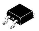
| 描述 | IC REG LDO ADJ 0.5A DPAK线性稳压器 500mA ADJ 1.2-37V Positive |
| 产品分类 | |
| 品牌 | ON Semiconductor |
| 产品手册 | |
| 产品图片 |
|
| rohs | 符合RoHS无铅 / 符合限制有害物质指令(RoHS)规范要求 |
| 产品系列 | 电源管理 IC,线性稳压器,ON Semiconductor LM317MDTG- |
| 数据手册 | |
| 产品型号 | LM317MDTG |
| PSRR/纹波抑制—典型值 | 80 dB |
| 产品目录页面 | |
| 产品种类 | 线性稳压器 |
| 供应商器件封装 | DPAK-3 |
| 其它名称 | LM317MDTG-ND |
| 包装 | 管件 |
| 商标 | ON Semiconductor |
| 安装类型 | 表面贴装 |
| 安装风格 | SMD/SMT |
| 封装 | Tube |
| 封装/外壳 | TO-252-3,DPak(2 引线+接片),SC-63 |
| 封装/箱体 | DPAK |
| 工作温度 | 0°C ~ 125°C |
| 工厂包装数量 | 75 |
| 最大工作温度 | + 125 C |
| 最大输入电压 | 40 V |
| 最小工作温度 | 0 C |
| 最小输入电压 | 4.2 V |
| 极性 | Positive |
| 标准包装 | 75 |
| 电压-跌落(典型值) | - |
| 电压-输入 | 最高 40 V |
| 电压-输出 | 1.2 V ~ 37 V |
| 电流-输出 | 500mA |
| 电流-限制(最小值) | - |
| 稳压器拓扑 | 正,可调式 |
| 稳压器数 | 1 |
| 系列 | LM317M |
| 线路调整率 | 0.07 % / V |
| 负载调节 | 1.5 % / V |
| 输出电压 | 1.2 V to 37 V |
| 输出电流 | 0.5 A |
| 输出端数量 | 1 |
| 输出类型 | Adjustable |


PDF Datasheet 数据手册内容提取
LM317M, NCV317MA, NCV317M Voltage Regulator - Adjustable Output, Positive 500 mA The LM317M is an adjustable three−terminal positive voltage www.onsemi.com regulator capable of supplying in excess of 500 mA over an output voltage range of 1.2V to 37 V. This voltage regulator is exceptionally easy to use and requires only two external resistors to set the output Heatsink surface voltage. Further, it employs internal current limiting, thermal connected to Pin 2 shutdown and safe area compensation, making it essentially blow−out proof. The LM317M serves a wide variety of applications including local, on−card regulation. This device also makes an especially simple TO−220AB adjustable switching regulator, a programmable output regulator, or by T SUFFIX connecting a fixed resistor between the adjustment and output, the CASE 221AB LM317M can be used as a precision current regulator. 1 Features 2 3 • Output Current in Excess of 500 mA • Output Adjustable between 1.2 V and 37 V SOT−223 • Internal Thermal Overload Protection ST SUFFIX 1 • CASE 318E 2 Internal Short Circuit Current Limiting 3 • Output Transistor Safe−Area Compensation • Floating Operation for High Voltage Applications • 4 Eliminates Stocking Many Fixed Voltages DPAK • NCV Prefix for Automotive and Other Applications Requiring DT SUFFIX 1 2 Unique Site and Control Change Requirements; AEC−Q100 CASE 369C 3 Qualified and PPAP Capable • These are Pb−Free Devices Heatsink Surface (shown as terminal 4 in case outline drawing) is connected to Pin 2. Vin Vout Vin LM317M Vout PIN ASSIGNMENT R1 1 Adjust 240 * IAdj Adjust + ** 2 Vout C0.i1n(cid:2)F C1.O0(cid:2)F 3 Vin R2 ORDERING INFORMATION See detailed ordering and shipping information in the package dimensions section on page 10 of this data sheet. (cid:2)* = Cin is required if regulator is located an appreciable distance from power supply filter. ** = CO is not needed for stability, however, it does improve transient response. DEVICE MARKING INFORMATION (cid:3) (cid:5) Vout(cid:2)1.25(cid:3)(cid:3)(cid:3)V(cid:3)(cid:3) 1(cid:4)RR21 (cid:4)IAdj(cid:3)(cid:3)R2 Sseecet iogne onne rpaal gme a1r1k ionfg t hiinsf odramtaa stihoene ti.n the device marking Since IAdj is controlled to less than 100 (cid:2)A, the error associated with this term is negligible in most applications. Figure 1. Simplified Application © Semiconductor Components Industries, LLC, 2014 1 Publication Order Number: October, 2019 − Rev. 26 LM317M/D
LM317M, NCV317MA, NCV317M MAXIMUM RATINGS (TA = 25°C, unless otherwise noted.) Rating Symbol Value Unit Input−Output Voltage Differential VI−VO 40 Vdc Power Dissipation (Package Limitation) (Note 1) Plastic Package, T Suffix, Case 221A TA = 25°C PD Internally Limited Thermal Resistance, Junction−to−Air (cid:3)JA 70 °C/W Thermal Resistance, Junction−to−Case (cid:3) 5.0 °C/W JC Plastic Package, DT Suffix, Case 369C TA = 25°C PD Internally Limited Thermal Resistance, Junction−to−Air (cid:3) 92 °C/W JA Thermal Resistance, Junction−to−Case (cid:3) 5.0 °C/W JC Plastic Package, ST Suffix, Case 318E TA = 25°C PD Internally Limited Thermal Resistance, Junction−to−Air (cid:3) 245 °C/W JA Thermal Resistance, Junction−to−Case (cid:3) 15 °C/W JC Maximum Junction Temperature TJMAX +150 °C Storage Temperature Range Tstg −65 to +150 °C Stresses exceeding those listed in the Maximum Ratings table may damage the device. If any of these limits are exceeded, device functionality should not be assumed, damage may occur and reliability may be affected. 1. Figure 25 provides thermal resistance versus PC board pad size. ELECTRICAL CHARACTERISTICS (VI − VO = 5.0 V; IO = 0.1 A, TJ = Tlow to Thigh (Note 2), unless otherwise noted.) LM317M/LM317MB/NCV317MB Characteristics Figure Symbol Min Typ Max Unit Line Regulation (Note 3) (TA = 25°C, 3.0 V ≤ VI − VO ≤ 40 V) 3 Regline − 0.01 0.04 %/V Load Regulation (Note 3) 4 Regload TA = 25°C, 10 mA ≤ IO ≤ 0.5 A VO ≤ 5.0 V − 5.0 25 mV VO ≥ 5.0 V − 0.1 0.5 % VO Adjustment Pin Current 5 IAdj − 50 100 (cid:2)A Adjustment Pin Current Change 3, 4 (cid:4)IAdj − 0.2 5.0 (cid:2)A 2.5 V ≤ VI − VO ≤ 40 V, 10 mA ≤ IL ≤ 0.5 A, PD ≤ Pmax Reference Voltage 5 Vref 1.20 1.25 1.30 V 3.0 V ≤VI − VO ≤ 40 V, 10 mA ≤ IL ≤ 0.5 A, PD ≤ Pmax Line Regulation 3.0 V ≤VI−VO ≤ 40 V (Note 3) 3 Regline − 0.02 0.07 %/V Load Regulation 10 mA ≤IO ≤0.5 A (Note 3) 4 Regload VO ≤5.0 V − 20 70 mV VO ≥ 5.0 V − 0.3 1.5 % VO Temperature Stability (Tlow ≤TJ ≤Thigh) 5 TS − 0.7 − % VO Minimum Load Current to Maintain Regulation (VI − VO = 40 V) 5 ILmin − 3.5 10 mA Maximum Output Current 5 Imax A VI − VO ≤ 15 V, PD ≤ Pmax 0.5 0.9 − VI − VO = 40 V, PD ≤Pmax, TA = 25°C 0.15 0.25 − RMS Noise, % of VO (TA = 25°C, 10 Hz ≤f ≤10 kHz) − N − 0.003 − % VO Ripple Rejection, VO = 10 V, f = 120 Hz (Note 4) 6 RR dB Without CAdj − 65 − CAdj = 10 (cid:2)F 66 80 − Thermal Shutdown (Note 5) − − − 180 − °C Long−Term Stability, TJ = Thigh (Note 6) 5 S − 0.3 1.0 %/1.0 TA= 25°C for End−point Measurements kHrs. 2. Tlow to Thigh = 0° to +125°C for LM317M Tlow to Thigh = −(cid:3)40° to +125°C for LM317MB, NCV317MB. 3. Load and line regulation are specified at constant junction temperature. Changes in VO due to heating effects must be taken into account separately. Pulse testing with low duty cycle is used. 4. CAdj, when used, is connected between the adjustment pin and ground. 5. Thermal characteristics are not subject to production test. 6. Since Long−Term Stability cannot be measured on each device before shipment, this specification is an engineering estimate of average stability from lot−to−lot. www.onsemi.com 2
LM317M, NCV317MA, NCV317M ELECTRICAL CHARACTERISTICS (VI − VO = 5.0 V; IO = 0.1 A, TJ = Tlow to Thigh (Note 7), unless otherwise noted.) LM317MA/LM317MAB/NCV317MAB Characteristics Figure Symbol Min Typ Max Unit Line Regulation (Note 8) (TA = 25°C, 3.0 V ≤ VI − VO ≤ 40 V) 3 Regline − 0.01 0.04 %/V Load Regulation (Note 8) 4 Regload TA = 25°C, 10 mA ≤ IO ≤ 0.5 A VO ≤ 5.0 V − 5.0 25 mV VO ≥ 5.0 V − 0.1 0.5 % VO Adjustment Pin Current 5 IAdj − 50 100 (cid:2)A Adjustment Pin Current Change 3, 4 (cid:4)IAdj − 0.2 5.0 (cid:2)A 2.5 V ≤ VI − VO ≤ 40 V, 10 mA ≤ IL ≤ 0.5 A, PD ≤ Pmax Reference Voltage 5 Vref 1.225 1.250 1.275 V 3.0 V ≤VI − VO ≤ 40 V, 10 mA ≤ IL ≤ 0.5 A, PD ≤ Pmax Line Regulation (Note 8) 3 Regline − 0.02 0.07 %/V 3.0 V ≤VI−VO ≤ 40 V Load Regulation (Note 8) 4 Regload 10 mA ≤IO ≤0.5 A VO ≤5.0 V − 20 70 mV VO ≥ 5.0 V − 0.3 1.5 % VO Temperature Stability (Tlow ≤TJ ≤Thigh) 5 TS − 0.7 − % VO Minimum Load Current to Maintain Regulation (VI − VO = 40 V) 5 ILmin − 3.5 10 mA Maximum Output Current 5 Imax A VI − VO ≤ 15 V, PD ≤ Pmax 0.5 0.9 − VI − VO = 40 V, PD ≤Pmax, TA = 25°C 0.15 0.25 − RMS Noise, % of VO (TA = 25°C, 10 Hz ≤f ≤10 kHz) − N − − − % VO Ripple Rejection, VO = 10 V, f = 120 Hz (Note 9) 6 RR dB Without CAdj − 65 − CAdj = 10 (cid:2)F 66 80 − Thermal Shutdown (Note 10) − − − 180 − °C Long−Term Stability, TJ = Thigh (Note 11) 5 S − 0.3 1.0 %/1.0 TA= 25°C for End−point Measurements kHrs. 7. Tlow to Thigh = 0° to +125°C for LM317MA Tlow to Thigh = −(cid:3)40° to +125°C for LM317MAB, NCV317MAB. 8. Load and line regulation are specified at constant junction temperature. Changes in VO due to heating effects must be taken into account separately. Pulse testing with low duty cycle is used. 9. CAdj, when used, is connected between the adjustment pin and ground. 10.Thermal characteristics are not subject to production test. 11.Since Long−Term Stability cannot be measured on each device before shipment, this specification is an engineering estimate of average stability from lot−to−lot. www.onsemi.com 3
LM317M, NCV317MA, NCV317M Vin 300 300 300 3.0k 300 70 6.8V 6.8V 350 18k 8.67k 500 130 400 5.1k 200k 180 180 2.0k 6.0k 10 60 1.25 6.3V pF 10 pF Vout 2.4k 12.8k 50 Adjust Figure 2. Representative Schematic Diagram VCC VOH - VOL Line Regulation (%/V) = x 100 * VOL VIH VOH VIL Vin Vout VOL LM317M Adjust R1 214%0 RL + Cin 0.1(cid:2)F IAdj CO 1.0(cid:2)F *(cid:4)Pulse Testing Required: R2 (cid:2)(cid:4)1% Duty Cycle is suggested. 1% Figure 3. Line Regulation and (cid:4)I /Line Test Circuit Adj www.onsemi.com 4
LM317M, NCV317MA, NCV317M Load Regulation (mV) = VO (min Load) -VO (max Load) VO (min Load) - VO (max Load) Load Regulation (% VO) = VO (min Load) X 100 VO (min Load) VO (max Load) Vin Vin Vout LM317M IL RL (max Load) Adjust R1 214%0 * RL (min Load) + Cin 0.1(cid:2)F IAdj CO 1.0(cid:2)F R2 1% *(cid:4)Pulse Testing Required: (cid:2)(cid:4)1% Duty Cycle is suggested. Figure 4. Load Regulation and (cid:4)I /Load Test Circuit Adj Vin Vout LM317M IL Adjust 240 VI R1 1% Vref RL IAdj + Cin 0.1(cid:2)F CO 1(cid:2)F VO ISET R2 1% *Pulse Testing Required: To Calculate R2: 1% Duty Cycle is suggested. Vout = ISET R2 + 1.250 V Assume ISET = 5.25 mA Figure 5. Standard Test Circuit 24V 14V Vin Vout Vout = 10 V LM317M f = 120 Hz D1 * Adjust R1 214%0 1N4002 RL + Cin 0.1(cid:2)F CO 1.0(cid:2)F VO ** + R2 11.%65K CAdj 10(cid:2)F (cid:4)*(cid:4)D1 Discharges CAdj if Output is Shorted to Ground. **CAdj provides an AC ground to the adjust pin. Figure 6. Ripple Rejection Test Circuit www.onsemi.com 5
LM317M, NCV317MA, NCV317M 90 %) E ( 0.4 Vin = 45 V CHANG 0.2 VILo =ut 5=. 05 .m0 AV to 40 mA ON (dB) 80 Without CAdj = 10 (cid:2)F GE 0 CTI OLTA -0.2 REJE 70 UTPUT V --00..46 VVILoi n=u t= 5= .1 050 .m 0V AV to 100 mA RIPPLE 60 IL = 100 mA Without CAdj , Oout -0.8 RR, fV =ou 1t 2=0 1 H0 zV V Vin = 14 V to 24 V Δ -1.0 50 -50 -25 0 25 50 75 100 125 150 -50 -25 0 25 50 75 100 125 150 TJ, JUNCTION TEMPERATURE (°C) TJ, JUNCTION TEMPERATURE (°C) Figure 7. Load Regulation Figure 8. Ripple Rejection 1.0 2.5 E G A T 0.80 OL IL = 500 mA NT (A) PUT VL (V) 2.0 RRE 0.60 OUTNTIA IL = 100 mA UTPUT CU 0.40 TJ = 25°C , INPUT-utDIFFERE 1.5 O o 1.0 I, out 0.20 TJ = 125°C V-Vin 0 0.5 0 10 20 30 40 50 -50 -25 0 25 50 75 100 125 150 Vin-Vout, INPUT-OUTPUT VOLTAGE DIFFERENTIAL (V) TJ, JUNCTION TEMPERATURE (°C) Figure 9. Current Limit Figure 10. Dropout Voltage 5.0 100 A) 4.5 90 NT CURRENT (m 4332....0505 TJ = 25°C REJECTION (dB) 87650000 IVVLoi n=u t= 4= 50 1. 0m.2 VA5 ±V 1.0 VPP CE 2.0 TJ = 125°C LE 40 S P E P UI 1.5 RI 30 , QB 1.0 RR, 20 I 0.5 10 0 10 20 30 40 10 100 1.0 k 10 k 100 k 1.0 M Vin-Vout, INPUT-OUTPUT VOLTAGE DIFFERENTIAL (Vdc) f, FREQUENCY (Hz) Figure 11. Minimum Operating Current Figure 12. Ripple Rejection versus Frequency www.onsemi.com 6
LM317M, NCV317MA, NCV317M 1.260 80 A) V) μNT ( 70 VVino u=t 6=. 2V5re Vf OLTAGE ( 1.250 N CURRE 6650 (cid:5)(cid:5)(cid:5)(cid:5)(cid:5)(cid:5)(cid:5)(cid:4)IILL == 1100 0m mAA REFERENCE V 11..224300 Vin = 4.2 V DJUSTMENT PI 554505 V, ref VILo =ut 5=. 0V mrefA , AAdj 40 I 1.220 35 -50 -25 0 25 50 75 100 125 150 -50 -25 0 25 50 75 100 125 150 TJ, JUNCTION TEMPERATURE (°C) TJ, JUNCTION TEMPERATURE (°C) Figure 13. Temperature Stability Figure 14. Adjustment Pin Current %) GE ( 0.4 Vin = 4.25 V to 41.25 V GE CHAN 0.20 IVLo =ut 5=. 0V mrefA μE (V) 10 Bandwidth 100 Hz to 10 kHz A G T A OL -0.2 LT 8.0 V O UT -0.4 E V P S OUT -0.6 NOI 6.0 , out -0.8 V Δ -1.0 4.0 -50 -25 0 25 50 75 100 125 150 -50 -25 0 25 50 75 100 125 150 TJ, JUNCTION TEMPERATURE (°C) TJ, JUNCTION TEMPERATURE (°C) Figure 15. Line Regulation Figure 16. Output Noise E G OLTA V) AGE 3.0 ΔV, OUTPUT VEoutDEVIATION (--11001.....505050 Vout = 10 V CL = 1.0 (cid:2)F ΔV, OUTPUT VOLToutDEVIATION (V)---12321.....000000 CL = 1.0 (cid:2)F; CCALd j= = 0 1.30 (cid:2)(cid:2)FF; CAdj = 10 (cid:2)F VVITNJoinL u = t== = 2 15 5150°0 CVm V A PUT VOLTAG ANGE (V)-101...055 TILJ = = 5 205 m°CA CVLin = 0 , LOADLRRENT (A)110...505 IL N H I U , InC 0 C 0 Vi 0 10 20 30 40 0 10 20 30 40 Δ t, TIME ((cid:2)s) t, TIME ((cid:2)s) Figure 17. Line Transient Response Figure 18. Load Transient Response www.onsemi.com 7
LM317M, NCV317MA, NCV317M APPLICATIONS INFORMATION Basic Circuit Operation External Capacitors The LM317M is a three−terminal floating regulator. In A 0.1 (cid:2)F disc or 1.0 (cid:2)F tantalum input bypass capacitor operation, the LM317M develops and maintains a nominal (C ) is recommended to reduce the sensitivity to input line in 1.25 V reference (V ) between its output and adjustment impedance. ref terminals. This reference voltage is converted to a The adjustment terminal may be bypassed to ground to programming current (I ) by R (see Figure 19), and this improve ripple rejection. This capacitor (C ) prevents PROG 1 Adj constant current flows through R to ground. The regulated ripple from being amplified as the output voltage is 2 output voltage is given by: increased. A 10(cid:2)F capacitor should improve ripple rejection about 15 dB at 120 Hz in a 10 V application. (cid:3) (cid:5) Vout(cid:2)Vref 1(cid:4)R2 (cid:4)IAdjR2 Although the LM317M is stable with no output R1 capacitance, like any feedback circuit, certain values of external capacitance can cause excessive ringing. An output Since the current from the terminal (IAdj) represents an capacitance (C ) in the form of a 1.0 (cid:2)F tantalum or 25 (cid:2)F O error term in the equation, the LM317M was designed to aluminum electrolytic capacitor on the output swamps this control I to less than 100 (cid:2)A and keep it constant. To do Adj effect and insures stability. this, all quiescent operating current is returned to the output terminal. This imposes the requirement for a minimum load Protection Diodes current. If the load current is less than this minimum, the When external capacitors are used with any IC regulator output voltage will rise. it is sometimes necessary to add protection diodes to prevent Since the LM317M is a floating regulator, it is only the the capacitors from discharging through low current points voltage differential across the circuit which is important to into the regulator. performance, and operation at high voltages with respect to Figure 20 shows the LM317M with the recommended ground is possible. protection diodes for output voltages in excess of 25 V or high capacitance values (C > 25 (cid:2)F, C > 5.0 (cid:2)F). Diode O Adj D prevents C from discharging thru the IC during an input 1 O Vin Vout short circuit. Diode D protects against capacitor C LM317M 2 Adj + discharging through the IC during an output short circuit. R1 The combination of diodes D1 and D2 prevents CAdj from Vref discharging through the IC during an input short circuit. Adjust IPROG Vout D1 IAdj R2 1N4002 Vref = 1.25 V Typical Vin Vout LM317M Vout + Figure 19. Basic Circuit Configuration Cin R1 D2 CO Adjust Load Regulation 1N4002 The LM317M is capable of providing extremely good R2 CAdj load regulation, but a few precautions are needed to obtain maximum performance. For best performance, the programming resistor (R ) should be connected as close to 1 the regulator as possible to minimize line drops which Figure 20. Voltage Regulator with effectively appear in series with the reference, thereby Protection Diodes degrading regulation. The ground end of R can be returned 2 near the load ground to provide remote ground sensing and improve load regulation. www.onsemi.com 8
LM317M, NCV317MA, NCV317M +25V Vout R1 VO IO LM317M Vin 1.25k D1 Adjust D1 1N4002 R2 1N914 Vin Vout * To provide current limiting of IO 500 D2 Vin LM317M Vout (cid:2)(cid:2)(cid:4)(cid:4)ttoh eth ceu srryesntet mlim gitrionugn ddio, dthee m souustr cbee otifed to 1N914 120 +1.0(cid:2)F (cid:2)(cid:4) a negative voltage below -7.25 V. Adjust 1N5314 R2 ≥ IVDrSeSf 720 MP1S.202k22 TCToLntrol Vref VSS* R1 = IOmax + IDSS Minimum Vout = 1.25 V VO < POV + 1.25 V + VSS ILmin - IP < IO < 500 mA - IP As shown O < IO < 495 mA D1 protects the device during an input short circuit. Figure 21. Adjustable Current Limiter Figure 22. 5 V Electronic Shutdown Regulator Iout Vin LM317M Vout Vout Vin LM317M VRo1ut R2 240 1N4001 Adjust IAdj Adjust 50k R2 MPS2907 +10(cid:2)F Ioutmax = R1V +re fR2 + IAdj (cid:6) R11.2 +5 RV2 5.0 mA < Iout < 500 mA Figure 23. Slow Turn−On Regulator Figure 24. Current Regulator 100 2.4 280 2.50 C/W) Free Air PD(max) for TA = 50°C Free Air PD(max) for TA = 50°C °-AIR ( 90 VMeoruticnatelldy 2.0 oz. Copper 2.0 240 VMeoruticnatelldy 2.0 oz. Copper 1.25 TO 80 ÎÎL Î 1.6 200 ÎÎLÎÎ0.83 - N Minimum Minimum O CTI 70 Size Pad LÎÎÎ 1.2 160 Size Pad ÎL ÎÎÎ0.63 UN ÎÎÎ ÎÎÎÎ J 60 0.8 120 0.50 E, C N TA 50 0.4 80 0.42 S SI R(cid:3)JA R(cid:3)JA E R 40 0 40 0.35 AL 0 5.0 10 15 20 25 30 0 5.0 10 15 20 25 30 M ER L, LENGTH OF COPPER (mm) L, LENGTH OF COPPER (mm) H T , JA Figure 25. DPAK Thermal Resistance and Maximum Figure 26. SOT−223 Thermal Resistance and Maximum θ R Power Dissipation versus PCB Copper Length Power Dissipation versus PCB Copper Length www.onsemi.com 9
LM317M, NCV317MA, NCV317M ORDERING INFORMATION Output Voltage Operating Temperature Device Tolerance Range Package Shipping† LM317MABDTG DPAK 75 Units / Rail (Pb−Free) LM317MABDTRKG DPAK 2500 / Tape & Reel (Pb−Free) NCV317MABDTRKG* TJ = −40°C to 125°C NCV317MABSTT3G* SOT−223 4000 / Tape & Reel 2% (Pb−Free) LM317MABTG TO−220 50 Units / Rail (Pb−Free) LM317MADTRKG TJ = 0°C to 125°C (PDb−PFArKee) 2500 / Tape & Reel LM317MBDTG DPAK 75 Units / Rail (Pb−Free) NCV317MBDTG* LM317MBDTRKG DPAK 2500 / Tape & Reel (Pb−Free) NCV317MBDTRKG* LM317MBSTT3G TJ = −40°C to 125°C SOT−223 4000 / Tape & Reel (Pb−Free) NCV317MBSTT3G* LM317MBTG TO−220 50 Units / Rail (Pb−Free) NCV317MBTG* 4% LM317MDTG DPAK 75 Units / Rail (Pb−Free) LM317MDTRKG DPAK 2500 / Tape & Reel (Pb−Free) TJ = 0°C to 125°C LM317MSTT3G SOT−223 4000 / Tape & Reel (Pb−Free) LM317MTG TO−220 50 Units / Rail (Pb−Free) †For information on tape and reel specifications, including part orientation and tape sizes, please refer to our Tape and Reel Packaging Specification Brochure, BRD8011/D. *NCV devices: Tlow = −40°C, Thigh = +125°C. Guaranteed by design. NCV Prefix for Automotive and Other Applications Requiring Unique Site and Control Change Requirements; AEC−Q100 Qualified and PPAP Capable. www.onsemi.com 10
LM317M, NCV317MA, NCV317M MARKING DIAGRAMS DPAK DT SUFFIX CASE 369C 317ABG 317MAG 317MBG 317MG ALYWW ALYWW ALYWW ALYWW TO−220 SOT−223 T SUFFIX ST SUFFIX CASE 221A CASE 318E AYW AYW AYW 317MA(cid:2) 317MB(cid:2) 317M(cid:2) LM LM LM (cid:2) (cid:2) (cid:2) 317MABT 317MBT 317MT AWLYWWG AWLYWWG AWLYWWG A = Assembly Location L, WL = Wafer Lot Y = Year WW, W = Work Week G or (cid:2) = Pb−Free Package (Note: Microdot may be in either location) www.onsemi.com 11
LM317M, NCV317MA, NCV317M PACKAGE DIMENSIONS TO−220, SINGLE GAUGE CASE 221AB ISSUE A NOTES: 1. DIMENSIONING AND TOLERANCING PER ANSI Y14.5M, 1982. −T− SPELAATNIENG 23.. CDOIMNETNRSOIOLLNI NZG D DEFIMINEENSS IAO ZNO: INNEC WHEHSE.RE ALL BODY AND B F C LEAD IRREGULARITIES ARE ALLOWED. 4. PRODUCT SHIPPED PRIOR TO 2008 HAD DIMENSIONS T S S = 0.045 - 0.055 INCHES (1.143 - 1.397 MM) 4 INCHES MILLIMETERS DIM MIN MAX MIN MAX A 0.570 0.620 14.48 15.75 Q A B 0.380 0.405 9.66 10.28 C 0.160 0.190 4.07 4.82 1 2 3 U D 0.025 0.035 0.64 0.88 H F 0.142 0.147 3.61 3.73 G 0.095 0.105 2.42 2.66 K H 0.110 0.155 2.80 3.93 Z J 0.018 0.025 0.46 0.64 K 0.500 0.562 12.70 14.27 L 0.045 0.060 1.15 1.52 N 0.190 0.210 4.83 5.33 L R Q 0.100 0.120 2.54 3.04 R 0.080 0.110 2.04 2.79 V J S 0.020 0.024 0.508 0.61 G T 0.235 0.255 5.97 6.47 U 0.000 0.050 0.00 1.27 D V 0.045 --- 1.15 --- N Z --- 0.080 --- 2.04 www.onsemi.com 12
LM317M, NCV317MA, NCV317M PACKAGE DIMENSIONS DPAK DT SUFFIX CASE 369C ISSUE F NOTES: A 1.DIMENSIONING AND TOLERANCING PER ASME Y14.5M, 1994. E C 2.CONTROLLING DIMENSION: INCHES. A 3.THERMAL PAD CONTOUR OPTIONAL WITHIN DI- b3 B MENSIONS b3, L3 and Z. c2 4.DIMENSIONS D AND E DO NOT INCLUDE MOLD FLASH, PROTRUSIONS, OR BURRS. MOLD FLASH, PROTRUSIONS, OR GATE BURRS SHALL 4 NOT EXCEED 0.006 INCHES PER SIDE. L3 Z 5.DIMENSIONS D AND E ARE DETERMINED AT THE D DETAIL A H 6.DOAUTTUEMRSM OA SATN EDX BT RAERME EDSE OTEFR TMHIEN EPDLA ASTT DICA TBUOMDY. 1 2 3 PLANE H. 7.OPTIONAL MOLD FEATURE. L4 INCHES MILLIMETERS NOTE 7 b2 c BOTTOM VIEW DIM MIN MAX MIN MAX A 0.086 0.094 2.18 2.38 e SIDE VIEW A1 0.000 0.005 0.00 0.13 b b 0.025 0.035 0.63 0.89 0.005 (0.13) M C b2 0.028 0.045 0.72 1.14 TOP VIEW b3 0.180 0.215 4.57 5.46 c 0.018 0.024 0.46 0.61 c2 0.018 0.024 0.46 0.61 H Z Z D 0.235 0.245 5.97 6.22 E 0.250 0.265 6.35 6.73 e 0.090 BSC 2.29 BSC L2 GPLAAUNGEE C SPELAATNIENG H 0.370 0.410 9.40 10.41 L 0.055 0.070 1.40 1.78 L1 0.114 REF 2.90 REF L2 0.020 BSC 0.51 BSC L A1 BOTTOM VIEW L3 0.035 0.050 0.89 1.27 L1 ALTERNATE L4 −−− 0.040 −−− 1.01 CONSTRUCTIONS Z 0.155 −−− 3.93 −−− DETAIL A ROTATED 90(cid:2) CW SOLDERING FOOTPRINT* 6.20 3.00 0.244 0.118 2.58 0.102 5.80 1.60 6.17 0.228 0.063 0.243 (cid:3) (cid:5) mm SCALE 3:1 inches *For additional information on our Pb−Free strategy and soldering details, please download the ON Semiconductor Soldering and Mounting Techniques Reference Manual, SOLDERRM/D. www.onsemi.com 13
LM317M, NCV317MA, NCV317M PACKAGE DIMENSIONS SOT−223 (TO−261) ST SUFFIX CASE 318E−04 ISSUE R (cid:2) (cid:2) www.onsemi.com 14
LM317M, NCV317MA, NCV317M ON Semiconductor and are trademarks of Semiconductor Components Industries, LLC dba ON Semiconductor or its subsidiaries in the United States and/or other countries. ON Semiconductor owns the rights to a number of patents, trademarks, copyrights, trade secrets, and other intellectual property. A listing of ON Semiconductor’s product/patent coverage may be accessed at www.onsemi.com/site/pdf/Patent−Marking.pdf. ON Semiconductor reserves the right to make changes without further notice to any products herein. ON Semiconductor makes no warranty, representation or guarantee regarding the suitability of its products for any particular purpose, nor does ON Semiconductor assume any liability arising out of the application or use of any product or circuit, and specifically disclaims any and all liability, including without limitation special, consequential or incidental damages. Buyer is responsible for its products and applications using ON Semiconductor products, including compliance with all laws, regulations and safety requirements or standards, regardless of any support or applications information provided by ON Semiconductor. “Typical” parameters which may be provided in ON Semiconductor data sheets and/or specifications can and do vary in different applications and actual performance may vary over time. All operating parameters, including “Typicals” must be validated for each customer application by customer’s technical experts. ON Semiconductor does not convey any license under its patent rights nor the rights of others. ON Semiconductor products are not designed, intended, or authorized for use as a critical component in life support systems or any FDA Class 3 medical devices or medical devices with a same or similar classification in a foreign jurisdiction or any devices intended for implantation in the human body. Should Buyer purchase or use ON Semiconductor products for any such unintended or unauthorized application, Buyer shall indemnify and hold ON Semiconductor and its officers, employees, subsidiaries, affiliates, and distributors harmless against all claims, costs, damages, and expenses, and reasonable attorney fees arising out of, directly or indirectly, any claim of personal injury or death associated with such unintended or unauthorized use, even if such claim alleges that ON Semiconductor was negligent regarding the design or manufacture of the part. ON Semiconductor is an Equal Opportunity/Affirmative Action Employer. This literature is subject to all applicable copyright laws and is not for resale in any manner. PUBLICATION ORDERING INFORMATION LITERATURE FULFILLMENT: N. American Technical Support: 800−282−9855 Toll Free ON Semiconductor Website: www.onsemi.com Literature Distribution Center for ON Semiconductor USA/Canada 19521 E. 32nd Pkwy, Aurora, Colorado 80011 USA Europe, Middle East and Africa Technical Support: Order Literature: http://www.onsemi.com/orderlit Phone: 303−675−2175 or 800−344−3860 Toll Free USA/Canada Phone: 421 33 790 2910 Fax: 303−675−2176 or 800−344−3867 Toll Free USA/Canada For additional information, please contact your local Email: orderlit@onsemi.com Sales Representative ◊ www.onsemi.com LM317M/D 15