ICGOO在线商城 > 集成电路(IC) > PMIC - 稳压器 - 线性 > LP3990MF-1.8/NOPB

 Datasheet下载
- 型号: LP3990MF-1.8/NOPB
- 制造商: Texas Instruments
- 库位|库存: xxxx|xxxx
- 要求:
| 数量阶梯 | 香港交货 | 国内含税 |
| +xxxx | $xxxx | ¥xxxx |
查看当月历史价格
查看今年历史价格
LP3990MF-1.8/NOPB产品简介:
ICGOO电子元器件商城为您提供LP3990MF-1.8/NOPB由Texas Instruments设计生产,在icgoo商城现货销售,并且可以通过原厂、代理商等渠道进行代购。 LP3990MF-1.8/NOPB价格参考¥2.20-¥5.43。Texas InstrumentsLP3990MF-1.8/NOPB封装/规格:PMIC - 稳压器 - 线性, Linear Voltage Regulator IC Positive Fixed 1 Output 1.8V 150mA SOT-23-5。您可以下载LP3990MF-1.8/NOPB参考资料、Datasheet数据手册功能说明书,资料中有LP3990MF-1.8/NOPB 详细功能的应用电路图电压和使用方法及教程。
Texas Instruments(德州仪器)的LP3990MF-1.8/NOPB是一款线性稳压器,属于PMIC(电源管理集成电路)系列。它具有低功耗、高精度和小型封装的特点,适用于多种便携式和低功耗应用场景。

 应用场景:

1. 便携式电子产品:
   - 该器件广泛应用于便携式设备中,如智能手机、平板电脑、可穿戴设备(如智能手表、健身追踪器)等。这些设备通常需要长时间续航,LP3990MF-1.8/NOPB的低静态电流(典型值为1.5µA)使其成为延长电池寿命的理想选择。

2. 物联网(IoT)设备:
   - 在物联网设备中,如传感器节点、智能家居设备、智能锁等,低功耗是关键要求。LP3990MF-1.8/NOPB能够提供稳定的1.8V输出电压,确保这些设备在低功耗模式下仍能正常工作,并且其小尺寸(SOT-23封装)有助于节省宝贵的PCB空间。

3. 医疗电子设备:
   - 医疗设备如血糖仪、心率监测仪、便携式超声设备等,对电源的稳定性和可靠性有严格要求。LP3990MF-1.8/NOPB的高精度输出电压和良好的瞬态响应性能,可以确保这些设备的准确性和稳定性,同时其低功耗特性也有助于延长电池寿命。

4. 工业自动化:
   - 在工业环境中,如传感器模块、无线通信模块、远程监控设备等,LP3990MF-1.8/NOPB可以为微控制器、传感器和其他低功耗组件提供稳定的电源。其宽输入电压范围(1.8V至5.5V)使其能够在不同的电源条件下正常工作,适应复杂的工业环境。

5. 消费类电子产品:
   - 对于一些消费类电子产品,如蓝牙耳机、电子阅读器、遥控器等,LP3990MF-1.8/NOPB的小型化和低功耗特性同样适用。它可以在保证设备性能的同时,减少电池消耗,提升用户体验。

总之,LP3990MF-1.8/NOPB凭借其低功耗、高精度和紧凑的设计,适用于各种对电源效率和稳定性有较高要求的应用场景,特别是在便携式和低功耗设备中表现出色。
| 参数 | 数值 |
| 产品目录 | 集成电路 (IC)半导体 |
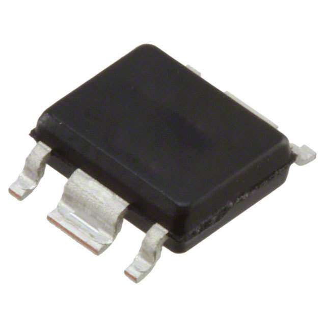
| 描述 | IC REG LDO 1.8V 0.15A SOT23-5低压差稳压器 150Ma CMOS LDO Reg |
| 产品分类 | |
| 品牌 | Texas Instruments |
| 产品手册 | |
| 产品图片 |
|
| rohs | 符合RoHS无铅 / 符合限制有害物质指令(RoHS)规范要求 |
| 产品系列 | 电源管理 IC,低压差稳压器,Texas Instruments LP3990MF-1.8/NOPB- |
| 数据手册 | |
| 产品型号 | LP3990MF-1.8/NOPB |
| PCN设计/规格 | |
| PSRR/纹波抑制—典型值 | 55 dB |
| 产品 | Linear Voltage Regulators |
| 产品目录页面 | |
| 产品种类 | 低压差稳压器 |
| 供应商器件封装 | SOT-23-5 |
| 其它名称 | LP3990MF-1.8/NOPBTR |
| 包装 | 带卷 (TR) |
| 商标 | Texas Instruments |
| 回动电压—最大值 | 200 mV |
| 安装类型 | 表面贴装 |
| 安装风格 | SMD/SMT |
| 封装 | Reel |
| 封装/外壳 | SC-74A,SOT-753 |
| 封装/箱体 | SOT-23-5 |
| 工作温度 | -40°C ~ 85°C |
| 工厂包装数量 | 1000 |
| 最大工作温度 | + 125 C |
| 最大输入电压 | 6 V |
| 最小工作温度 | - 40 C |
| 最小输入电压 | 2 V |
| 标准包装 | 1,000 |
| 电压-跌落(典型值) | - |
| 电压-输入 | 2 V ~ 6 V |
| 电压-输出 | 1.8V |
| 电流-输出 | 150mA |
| 电流-限制(最小值) | - |
| 稳压器拓扑 | 正,固定式 |
| 稳压器数 | 1 |
| 类型 | Accurate Output Voltage |
| 系列 | LP3990 |
| 线路调整率 | 0.02 % |
| 设计资源 | http://www.digikey.com/product-highlights/cn/zh/texas-instruments-webench-design-center/3176 |
| 负载调节 | 0.003 %/mA |
| 输出电压 | 1.8 V |
| 输出电压容差 | +/- 4 % |
| 输出电流 | 150 mA |
| 输出端数量 | 1 Output |
| 输出类型 | Fixed |


- 商务部:美国ITC正式对集成电路等产品启动337调查
- 曝三星4nm工艺存在良率问题 高通将骁龙8 Gen1或转产台积电
- 太阳诱电将投资9.5亿元在常州建新厂生产MLCC 预计2023年完工
- 英特尔发布欧洲新工厂建设计划 深化IDM 2.0 战略
- 台积电先进制程称霸业界 有大客户加持明年业绩稳了
- 达到5530亿美元!SIA预计今年全球半导体销售额将创下新高
- 英特尔拟将自动驾驶子公司Mobileye上市 估值或超500亿美元
- 三星加码芯片和SET,合并消费电子和移动部门,撤换高东真等 CEO
- 三星电子宣布重大人事变动 还合并消费电子和移动部门
- 海关总署:前11个月进口集成电路产品价值2.52万亿元 增长14.8%


PDF Datasheet 数据手册内容提取
Product Sample & Technical Tools & Support & Folder Buy Documents Software Community LP3990 SNVS251J–MAY2004–REVISEDSEPTEMBER2014 LP3990 150-mA Linear Voltage Regulator for Digital Applications 1 Features 3 Description • 1%VoltageAccuracyatRoomTemperature The LP3990 regulator is designed to meet the 1 requirements of portable, battery-powered systems • StablewithCeramicCapacitor providing an accurate output voltage, low-noise, and • LogicControlledEnable low-quiescent current. The LP3990 will provide a 0.8- • NoNoiseBypassCapacitorRequired V output from the low input voltage of 2 V at up to a 150-mA load current. When switched into shutdown • Thermal-OverloadandShort-CircuitProtection mode via a logic signal at the enable pin (EN), the • InputVoltageRange,2Vto6V powerconsumptionisreducedtovirtuallyzero. • OutputVoltageRange,0.8Vto3.3V The LP3990 is designed to be stable with space- • OutputCurrent,150mA savingceramiccapacitorswithvaluesaslowas1µF. • OutputStable-Capacitors,1 µF Performance is specified for a –40°C to 125°C • VirtuallyZeroIQ(Disabled),<10nA junctiontemperaturerange. • VeryLowI (Enabled),43µA Q For output voltages other than 0.8 V, 1.2 V, 1.35 V, • LowOutputNoise,150µVRMS 1.5 V, 1.8 V, 2.5 V, 2.8 V, or 3.3 V, please contact • PSRR,55dBat1kHz theTexasInstrumentssalesoffice. • FastStart-Up,105 µs DeviceInformation(1) 2 Applications PARTNUMBER PACKAGE BODYSIZE(NOM) DSBGA(4) 1.324mmx1.045mm(MAX) • CellularHandsets LP3990 WSON(6) 2.90mmx1.60mm • Hand-HeldInformationAppliances SOT-23(5) 3.00mmx3.00mm (1) For all available packages, see the orderable addendum at theendofthedatasheet. SimplifiedSchematic V V IN OUT IN OUT C C IN OUT 1 µF LP3990 1 µF V EN EN ON OFF GND GND GND 1 An IMPORTANT NOTICE at the end of this data sheet addresses availability, warranty, changes, use in safety-critical applications, intellectualpropertymattersandotherimportantdisclaimers.PRODUCTIONDATA.
LP3990 SNVS251J–MAY2004–REVISEDSEPTEMBER2014 www.ti.com Table of Contents 1 Features.................................................................. 1 7.3 FeatureDescription...................................................9 2 Applications........................................................... 1 7.4 DeviceFunctionalModes........................................10 3 Description............................................................. 1 8 ApplicationandImplementation........................ 11 4 RevisionHistory..................................................... 2 8.1 ApplicationInformation............................................11 8.2 TypicalApplication .................................................11 5 PinConfigurationandFunctions......................... 3 9 PowerSupplyRecommendations...................... 14 6 Specifications......................................................... 4 10 Layout................................................................... 14 6.1 AbsoluteMaximumRatings......................................4 6.2 HandlingRatings......................................................4 10.1 LayoutGuidelines.................................................14 6.3 RecommendedOperatingConditions.......................4 10.2 LayoutExamples...................................................15 6.4 ThermalInformation..................................................4 10.3 DSBGAMounting..................................................16 6.5 ElectricalCharacteristics...........................................5 10.4 DSBGALightSensitivity.......................................16 6.6 OutputCapacitor,RecommendedSpecifications.....6 11 DeviceandDocumentationSupport................. 17 6.7 TimingRequirements................................................6 11.1 Trademarks...........................................................17 6.8 TypicalPerformanceCharacteristics........................7 11.2 ElectrostaticDischargeCaution............................17 7 DetailedDescription.............................................. 9 11.3 Glossary................................................................17 7.1 Overview...................................................................9 12 Mechanical,Packaging,andOrderable Information........................................................... 17 7.2 FunctionalBlockDiagram.........................................9 4 Revision History ChangesfromRevisionI(May2013)toRevisionJ Page • AddedDeviceInformationandHandlingRatingtables,FeatureDescription,DeviceFunctionalModes,Application andImplementation,PowerSupplyRecommendations,Layout,DeviceandDocumentationSupport,and Mechanical,Packaging,andOrderableInformationsections;movedsomecurvestoApplicationCurvessection..............1 2 SubmitDocumentationFeedback Copyright©2004–2014,TexasInstrumentsIncorporated ProductFolderLinks:LP3990
LP3990 www.ti.com SNVS251J–MAY2004–REVISEDSEPTEMBER2014 5 Pin Configuration and Functions 4Pins 5Pins DSBGA(YZR) SOT-23(DBV) EN IN IN EN EN GND IN A2 B2 B2 A2 3 2 1 A1 B1 B1 A1 GND OUT OUT GND TOP VIEW BOTTOM VIEW 4 5 N/C OUT WSON(NGG) 6Pins IN EN N/C N/C EN IN 6 5 4 4 5 6 (Thermal DAP) Thermal DAP 1 2 3 3 2 1 OUT GND N/C N/C GND OUT TOP VIEW BOTTOM VIEW PinFunctions PIN DSBGA SOT-23 WSON I/O DESCRIPTION NAME YZR DBV NGG GND A1 2 2 — CommonGround. EN A2 3 5 EnableInput;EnablestheRegulatorwhen≥0.95V. I DisablestheRegulatorwhen≤0.4V. EnableInputhas1-MΩ(typical)pull-downresistortoGND. OUT B1 5 1 Voltageoutput.A1-µFLowESRCapacitorshouldbeconnectedtothisPin. O Connectthisoutputtotheloadcircuit. IN B2 1 6 I VoltagesupplyInput.A1-µFcapacitorshouldbeconnectedatthisinput. 4 3 I Nointernalconnection. N/C N/A 4 I Nointernalconnection. N/A N/C Pad — Thermalpad.ConnecttoPin2. Copyright©2004–2014,TexasInstrumentsIncorporated SubmitDocumentationFeedback 3 ProductFolderLinks:LP3990
LP3990 SNVS251J–MAY2004–REVISEDSEPTEMBER2014 www.ti.com 6 Specifications 6.1 Absolute Maximum Ratings(1)(2)(3) overoperatingfree-airtemperaturerange(unlessotherwisenoted) MIN MAX UNIT Inputvoltage –0.3 6.5 Outputvoltage –0.3 Note(4) V ENABLEinputvoltage –0.3 6.5 Continuouspowerdissipationinternallylimited Note(5) (1) StressesbeyondthoselistedunderAbsoluteMaximumRatingsmaycausepermanentdamagetothedevice.Thesearestressratings only,whichdonotimplyfunctionaloperationofthedeviceattheseoranyotherconditionsbeyondthoseindicatedunderRecommended OperatingConditions.Exposuretoabsolute-maximum-ratedconditionsforextendedperiodsmayaffectdevicereliability. (2) IfMilitary/Aerospacespecifieddevicesarerequired,pleasecontacttheTISalesOffice/Distributorsforavailabilityandspecifications. (3) AllvoltagesarewithrespecttothepotentialattheGNDpin. (4) ThelowerofV +0.3Vor6.5V. IN (5) Internalthermalshutdowncircuitryprotectsthedevicefrompermanentdamage. 6.2 Handling Ratings MIN MAX UNIT T Storagetemperaturerange –65 150 °C stg Humanbodymodel(HBM),perANSI/ESDA/JEDECJS-001,all pins(1) –2000 2000 V Electrostaticdischarge Chargeddevicemodel(CDM),perJEDECspecificationJESD22- V (ESD) 250 1500 C101,allpins Machinemodel –200 200 (1) JEDECdocumentJEP155statesthat2000-VHBMallowssafemanufacturingwithastandardESDcontrolprocess. 6.3 Recommended Operating Conditions overoperatingfree-airtemperaturerange(unlessotherwisenoted) MIN NOM MAX UNIT Inputvoltage,V 2 6 IN V Enableinputvoltage,V 0.0 V EN IN Junctiontemperature,T (1) –40 125 °C J (1) T =(T +(R ×P )) J(max) A(max) θJA D(max) 6.4 Thermal Information LP3990 THERMALMETRIC(1) YZR(DSBGA) DBV(SOT-23) NGG(WSON) UNIT 4PINS 5PINS 6PINS R Junction-to-ambientthermalresistance 188.9 165.2 53.9 θJA R Junction-to-case(top)thermalresistance 1.0 69.9 51.2 θJC(top) R Junction-to-boardthermalresistance 105.3 27.3 28.2 θJB °C/W ψ Junction-to-topcharacterizationparameter 0.7 1.8 0.6 JT ψ Junction-to-boardcharacterizationparameter 105.2 26.8 28.3 JB R Junction-to-case(bottom)thermalresistance N/A N/A 8.1 θJC(bot) (1) Formoreinformationabouttraditionalandnewthermalmetrics,seetheICPackageThermalMetricsapplicationreport,SPRA953. 4 SubmitDocumentationFeedback Copyright©2004–2014,TexasInstrumentsIncorporated ProductFolderLinks:LP3990
LP3990 www.ti.com SNVS251J–MAY2004–REVISEDSEPTEMBER2014 6.5 Electrical Characteristics(1)(2) Unlessotherwisenoted,V =950mV,V =V +1VorV =2V,whicheverishigher.C =1µF,I =1mA,C = EN IN OUT IN IN OUT OUT 0.47µF. PARAMETER TESTCONDITIONS MIN TYP MAX UNIT V Inputvoltage Note (3),T =25°C 2 6 V IN J DSBGA –1 1% I =1mA LOAD WQFN –1.5% 1.5% T =25°C J SOT-23 –1.5% 1.5% Outputvoltagetolerance DSBGA –2.5% 2.5% Overfulllineandload WQFN –3% 3% regulation SOT-23 –4% 4% Lineregulationerror V =(V +1V)to6V 0.1 0.02 0.1 %/V IN OUT(NOM) ΔVOUT VOUT=0.8Vto1.95 V –0.005 0.002 0.005 DSBGA V =0.8Vto1.95 OUT I =1mA V –0.008 0.003 0.008 Loadregulationerror tOoU1T50mA WQFN,SOT-23 %/mA V =2Vto3.3V OUT –0.002 0.0005 0.002 DSBGA V =2Vto3.3V OUT –0.005 0.002 0.005 WQFN,SOT-23 V Dropoutvoltage I =150mA(4) (5) 120 200 mV DO OUT I Loadcurrent Note (5)(6),T =25°C 0 µA LOAD J V =950mV,I =0mA 43 80 EN OUT I Quiescentcurrent V =950mV,I =150mA 65 120 µA Q EN OUT V =0.4V(outputdisabled),T =25°C 0.002 0.2 EN J I Shortcircuitcurrentlimit Note (7) 550 1000 SC mA I Maximumoutputcurrent 150 OUT PowerSupplyRejection ƒ=1kHz,IOUT=1mAto150mA 55 PSRR dB Ratio ƒ=10kHz,I =150mA 35 OUT V =0.8V 60 OUT e Outputnoisevoltage(5) BW=10Hzto100 V =1.5V 125 µV η kHz OUT RMS V =3.3V 180 OUT Junctiontemperature(T)risinguntilthe T Thermalshutdown outputisdisabled J 155 °C SHUTDOWN junctiontemperature Hysteresis 15 (1) AllvoltagesarewithrespecttothedeviceGNDterminal,unlessotherwisestated. (2) MinimumandMaximumlimitsareensuredthroughtest,design,orstatisticalcorrelationovertheoperatingjunctiontemperaturerange (T)of–40°Cto125°C,unlessotherwisestated.TypicalvaluesrepresentthemostlikelyparametricnormatT =25°C,andare J J providedforreferencepurposesonly. (3) V =V +0.5V,or2V,whicheverishigher. IN(MIN) OUT(NOM) (4) Dropoutvoltageisvoltagedifferencebetweeninputandoutputatwhichtheoutputvoltagedropsto100mVbelowitsnominalvalue. Thisparameterappliesonlyforoutputvoltagesabove2V. (5) Thiselectricalspecificationisverifiedbydesign. (6) Thedevicemaintainstheregulatedoutputvoltagewithouttheload. (7) Short-circuitcurrentismeasuredwithV pulledto0VandV worstcase=6V. OUT IN Copyright©2004–2014,TexasInstrumentsIncorporated SubmitDocumentationFeedback 5 ProductFolderLinks:LP3990
LP3990 SNVS251J–MAY2004–REVISEDSEPTEMBER2014 www.ti.com Electrical Characteristics(1)(2) (continued) Unlessotherwisenoted,V =950mV,V =V +1VorV =2V,whicheverishigher.C =1µF,I =1mA,C = EN IN OUT IN IN OUT OUT 0.47µF. PARAMETER TESTCONDITIONS MIN TYP MAX UNIT ENABLECONTROLCHARACTERISTICS V =0V(Outputisdisabled) IEN(8) MataExNimpuimn inputcurrent TJEN=25°C 0.001 0.1 µA V =6V 2.5 6 10 EN V =2Vto6V IN V Lowinputthreshold V fallingfrom≥V untiltheoutputis 0.4 IL EN IH disabled V V =2Vto6V IN V Highinputthreshold V risingfrom≤V untiltheoutputis 0.95 IH EN IL enabled (8) ENABLEPinhas1-MΩ(typical)resistorconnectedtoGND. 6.6 Output Capacitor, Recommended Specifications(1) PARAMETER TESTCONDITIONS MIN TYP MAX UNIT Capacitance(2) 0.7(3) 1 500 µF C Outputcapacitance OUT ESR 5 mΩ (1) Unlessotherwisespecified,valuesandlimitsapplyforT =25°C. J (2) Thefulloperatingconditionsfortheapplicationshouldbeconsideredwhenselectingasuitablecapacitortoensurethattheminimum valueofcapacitanceisalwaysmet.RecommendedcapacitortypeisX7R.However,dependentonapplication,X5R,Y5V,andZ5Ucan alsobeused.(SeeDetailedDesignProcedure.) (3) Limitappliesoverthefulloperatingjunctiontemperaturerange(T)of−40°Cto125°C. J 6.7 Timing Requirements MIN NOM(1) MAX(2) UNIT V =0.8V 80 150 FromV ↑V to OUT EN IH T Turnontime (3) V 95%level V =1.5V 105 200 µs ON OUT OUT (V )to6V) IN(MIN V =3.3V 175 250 OUT Linetransientresponse T =T =30µs(3), mV(pk- rise fall 8 16 (ΔV ) ΔV =600mV pk) OUT IN Transient response Loadtransientresponse Trise=Tfall=1µs(3), I =1mAto150mA 55 100 mV (ΔV ) OUT OUT C =1µF OUT (1) NomvaluesapplyforT =25°C. J (2) Maximumlimitsapplyoverthefulloperatingjunctiontemperature(T)rangeof−40°Cto125°C. J (3) Thiselectricalspecificationisverifiedbydesign. 6 SubmitDocumentationFeedback Copyright©2004–2014,TexasInstrumentsIncorporated ProductFolderLinks:LP3990
LP3990 www.ti.com SNVS251J–MAY2004–REVISEDSEPTEMBER2014 6.8 Typical Performance Characteristics Unlessotherwisespecified,C =1µFceramic,C =0.47µFceramic,V =V +1V,T =25°C,V =1.5V; IN OUT IN OUT(NOM) A OUT(NOM) V =V . EN IN 2.00 80 1.50 70 TJ = 125°C )%( EGNAHC TU -0010....05050000 )A( TNERRUPC DN 34560000 TJ = -40°C VO -1.00 UOR 20 TJ = 25°C G -1.50 10 -2.00 0 -40 -25 0 25 50 75 100 125 0 25 50 75 100 125 150 TEMPERATURE (°C) LOAD CURRENT (mA) Figure1.OutputVoltageChangevsTemperature Figure2.GroundCurrentvsLoadCurrent 100 100 90 90 80 80 )A 70 )A 70 P P ( I D 60 ( I D 60 N TJ = 125°C N TJ = 125°C G 50 G 50 TJ = 25°C TJ = 25°C 40 40 30 TJ = -40°C 30 TJ = -40°C 20 20 2 2.5 3 3.5 4 4.5 5 5.5 6 2 2.5 3 3.5 4 4.5 5 5.5 6 VIN VIN I =0mA I =1mA LOAD LOAD Figure3.GroundCurrentvsV Figure4.GroundCurrentvsV IN IN 100 VIN = 2.5V 90 800 80 TJ = 125°C T 600 N )A( I Dµ 6700 TJ = 25°C CURRE(mA) 420000 NG 50 TJ = -40°C 0 40 30 UTDiv) 20 VO1V/ 2 2.5 3 3.5 4 4.5 5 5.5 6 ( VIN TIME (100 Ps/DIV) I =150mA LOAD Figure5.GroundCurrentvsV Figure6.ShortCircuitCurrent IN Copyright©2004–2014,TexasInstrumentsIncorporated SubmitDocumentationFeedback 7 ProductFolderLinks:LP3990
LP3990 SNVS251J–MAY2004–REVISEDSEPTEMBER2014 www.ti.com Typical Performance Characteristics (continued) Unlessotherwisespecified,C =1µFceramic,C =0.47µFceramic,V =V +1V,T =25°C,V =1.5V; IN OUT IN OUT(NOM) A OUT(NOM) V =V . EN IN VIN = 6V CIN = 1 PF 800 COUT = 0.47 PF IL = 1 to 150 mA 600 NT V) URRE(mA) 400 V(IN 3.1 C 200 2.5 0 v) TDi VOUmV/ VOUT1V/Div) ' (10 ( TIME (100 Ps/DIV) TIME (100 Ps/DIV) Figure7.ShortCircuitCurrent Figure8.LineTransient 0 0 -10 -10 COUT = 0.47 PF COUT = 1 PF )B -20 )B -20 d( NOIT --4300 IL = 1 mA d( NOIT --4300 ILOAD = 150 mA C C EJER E --6500 COUT = 1 PF EJER E --6500 COUT = 0.47 PF LP -70 LP -70 PIR -80 PIR -80 -90 -90 100 1k 10k 100k 1M 100 1k 10k 100k 1M FREQUENCY (Hz) FREQUENCY (Hz) Figure9.PowerSupplyRejectionRatio Figure10.PowerSupplyRejectionRatio IL = 1 mA 10 Div) VOUT = 3.3V UTV/ Om V 500 )zH 1 VOUT = 1.5V ( /V P ( E S ION 0.1 v) VENV/Di 0.01 (1 0.1 1 10 100 TIME (50 Ps/DIV) FREQUENCY (kHz) Figure11.EnableStart-UpTime Figure12.NoiseDensity 8 SubmitDocumentationFeedback Copyright©2004–2014,TexasInstrumentsIncorporated ProductFolderLinks:LP3990
LP3990 www.ti.com SNVS251J–MAY2004–REVISEDSEPTEMBER2014 7 Detailed Description 7.1 Overview Designed meet the requirements of portable, battery-powered digital systems providing an accurate output voltage with fast start-up. When disabled via a low logic signal at the enable pin (EN), the power consumption is reducedtovirtuallyzero The LP3990 is designed to perform with a single 1-μF input capacitor and a single 1-μF ceramic output capacitor. 7.2 Functional Block Diagram LP3990 IN OUT Current Thermal Limit Shutdown + ON OFF VREF 800 mV EN 1 M(cid:13)(cid:3) GND 7.3 Feature Description 7.3.1 Enable(EN) The LP3990 Enable (EN) pin is internally held low by a 1-MΩ resistor to GND. The EN pin voltage must be higher than the V threshold to ensure that the device is fully enabled under all operating conditions. The EN pin IH voltage must be lower than the V threshold to ensure that the device is fully disabled. If the EN pin is left open IL theLP3990outputwillbedisabled. 7.3.2 ThermalOverloadProtection(T ) SD Thermal Shutdown disables the output when the junction temperature rises to approximately 155°C which allows the device to cool. When the junction temperature cools to approximately 140°C, the output circuitry enables. Based on power dissipation, thermal resistance, and ambient temperature, the thermal protection circuit may cycle on and off. This thermal cycling limits the dissipation of the regulator and protects it from damage as a resultofoverheating. The Thermal Shutdown circuitry of the LP3990 has been designed to protect against temporary thermal overload conditions. The Thermal Shutdown circuitry was not intended to replace proper heat-sinking. Continuously runningtheLP3990deviceintothermalshutdownmaydegradedevicereliability. Copyright©2004–2014,TexasInstrumentsIncorporated SubmitDocumentationFeedback 9 ProductFolderLinks:LP3990
LP3990 SNVS251J–MAY2004–REVISEDSEPTEMBER2014 www.ti.com 7.4 Device Functional Modes 7.4.1 Enable(EN) TheLP3990ENpinisinternallyheldlowbya1-MΩresistortoGND.TheENpinvoltagemustbehigherthanthe V thresholdtoensurethatthedeviceisfullyenabledunderalloperatingconditions. IH 7.4.2 MinimumOperatingInputVoltage(V ) IN The LP3990 does not include any dedicated UVLO circuitry. The LP3990 internal circuitry is not fully functional untilV isatleast2V.TheoutputvoltageisnotregulateduntilV ≥(V +V ),or2V,whicheverishigher. IN IN OUT DO 10 SubmitDocumentationFeedback Copyright©2004–2014,TexasInstrumentsIncorporated ProductFolderLinks:LP3990
LP3990 www.ti.com SNVS251J–MAY2004–REVISEDSEPTEMBER2014 8 Application and Implementation NOTE Information in the following applications sections is not part of the TI component specification, and TI does not warrant its accuracy or completeness. TI’s customers are responsible for determining suitability of components for their purposes. Customers should validateandtesttheirdesignimplementationtoconfirmsystemfunctionality. 8.1 Application Information The LP3990 is a linear voltage regulator for digital applications designed to be stable with space-saving ceramic capacitorsassmallas1µF. 8.2 Typical Application Figure13showsthetypicalapplicationcircuitfortheLP3990.Theinputandoutputcapacitancesmayneedtobe increasedabovethe1μFshownforsomeapplications. VIN VOUT IN OUT CIN COUT 1 µF LP3990 1 µF VEN EN ON OFF GND GND GND Figure13. LP3990TypicalApplication 8.2.1 DesignRequirements DESIGNPARAMETER EXAMPLEVALUE Inputvoltagerange 2Vto6V Outputvoltage 1.8V Outputcurrent 100mA Outputcapacitorrange 1µF Input/outputcapacitorESRrange 5mΩto500mΩ 8.2.2 DetailedDesignProcedure Tobeginthedesignprocess,determinethefollowing: • Availableinputvoltagerange • Outputvoltageneeded • Outputcurrentneeded • Inputandoutputcapacitors 8.2.2.1 PowerDissipationandDeviceOperation The permissible power dissipation for any package is a measure of the capability of the device to pass heat from the power source, the junctions of the IC, to the ultimate heat sink, the ambient environment. Thus, the power dissipation is dependent on the ambient temperature and the thermal resistance across the various interfaces betweenthediejunctionandambientair. ThemaximumallowablepowerdissipationforthedeviceinagivenpackagecanbecalculatedusingEquation1: P =((T -T )/R ) (1) D-MAX J-MAX A θJA Copyright©2004–2014,TexasInstrumentsIncorporated SubmitDocumentationFeedback 11 ProductFolderLinks:LP3990
LP3990 SNVS251J–MAY2004–REVISEDSEPTEMBER2014 www.ti.com TheactualpowerbeingdissipatedinthedevicecanberepresentedbyEquation2: P =(V -V )xI (2) D IN OUT OUT These two equations establish the relationship between the maximum power dissipation allowed due to thermal consideration, the voltage drop across the device, and the continuous current capability of the device. These two equationsshouldbeusedtodeterminetheoptimumoperatingconditionsforthedeviceintheapplication. In applications where lower power dissipation (P ) and/or excellent package thermal resistance (R ) is present, D θJA themaximumambienttemperature(T )maybeincreased. A-MAX In applications where high power dissipation and/or poor package thermal resistance is present, the maximum ambient temperature (T ) may have to be derated. T is dependent on the maximum operating junction A-MAX A-MAX temperature (T = 125°C), the maximum allowable power dissipation in the device package in the J-MAX-OP application (P ), and the junction-to ambient thermal resistance of the part/package in the application (R ), D-MAX θJA asgivenbyEquation3: T =(T –(R ×P )) (3) A-MAX J-MAX-OP θJA D-MAX Alternately, if T can not be derated, the P value must be reduced. This can be accomplished by reducing A-MAX D V in the 'V –V ' term as long as the minimum V is met, or by reducing the I term, or by some IN IN OUT IN OUT combinationofthetwo. 8.2.2.2 ExternalCapacitors In common with most regulators, the LP3990 requires external capacitors for regulator stability. The LP3990 is specifically designed for portable applications requiring minimum board space and smallest components. These capacitorsmustbecorrectlyselectedforgoodperformance. 8.2.2.3 InputCapacitor An input capacitor is required for stability. It is recommended that a 1-µF capacitor be connected between the LP3990INpinandGNDpin(thiscapacitancevaluemaybeincreasedwithoutlimit). This capacitor must be located a distance of not more than 1 cm from the IN pin and returned to a clean analogueground.Anygoodqualityceramic,tantalum,orfilmcapacitormaybeusedattheinput. Important: To ensure stable operation it is essential that good PCB design practices are employed to minimize ground impedance and keep input inductance low. If these conditions cannot be met, or if long leads are used to connect the battery or other power source to the LP3990, then it is recommended that the input capacitor is increased. Also, tantalum capacitors can suffer catastrophic failures due to surge current when connected to a low-impedance source of power (like a battery or a very large capacitor). If a tantalum capacitor is used at the input,itmustbeensuredbythemanufacturertohaveasurgecurrentratingsufficientfortheapplication. There are no requirements for the ESR (Equivalent Series Resistance) on the input capacitor, but tolerance and temperature coefficient must be considered when selecting the capacitor to ensure the capacitance will remain approximately1 µFovertheentireoperatingtemperaturerange. 8.2.2.4 OutputCapacitor The LP3990 is designed specifically to work with very small ceramic output capacitors. A 1-µF ceramic capacitor (temperature types Z5U, Y5V or X7R/X5R) with ESR between 5 mΩ to 500 mΩ, is suitable in the LP3990 applicationcircuit. ForthisdevicetheoutputcapacitorshouldbeconnectedbetweentheOUTpinandGNDpin. It is also possible to use tantalum or film capacitors at the device output, but these are not as attractive for reasonsofsizeandcost(seeCapacitorCharacteristics). The output capacitor must meet the requirement for the minimum value of capacitance and also have an ESR valuethatiswithintherange5mΩ to500mΩ forstability. 8.2.2.5 No-LoadStability The LP3990 will remain stable and in regulation with no external load. This is an important consideration in some circuits,forexampleCMOSRAMkeep-aliveapplications. 12 SubmitDocumentationFeedback Copyright©2004–2014,TexasInstrumentsIncorporated ProductFolderLinks:LP3990
LP3990 www.ti.com SNVS251J–MAY2004–REVISEDSEPTEMBER2014 8.2.2.6 CapacitorCharacteristics The LP3990 is designed to work with ceramic capacitors on the output to take advantage of the benefits they offer. For capacitance values in the range of 0.47 µF to 4.7 µF, ceramic capacitors are the smallest, least expensive and have the lowest ESR values, thus making them best for eliminating high frequency noise. The ESR of a typical 1-µF ceramic capacitor is in the range of 20 mΩ to 40 mΩ, which easily meets the ESR requirementforstabilityfortheLP3990. For both input and output capacitors, careful interpretation of the capacitor specification is required to ensure correct device operation. The capacitor value can change greatly, depending on the operating conditions and capacitortype. Inparticular,theoutputcapacitorselectionshouldtakeaccountofallthecapacitorparameters,toensurethatthe specification is met within the application. The capacitance can vary with DC bias conditions as well as temperature and frequency of operation. Capacitor values will also show some decrease over time due to aging. The capacitor parameters are also dependant on the particular case size, with smaller sizes giving poorer performance figures in general. As an example, Figure 14 shows a typical graph comparing different capacitor casesizesinaCapacitancevs.DCBiasplot.Asshowninthegraph,increasingtheDCBiasconditioncanresult in the capacitance value falling below the minimum value given in the recommended capacitor specifications table (0.7 µF in this case). Note that the graph shows the capacitance out of spec for the 0402 case size capacitorathigherbiasvoltages.Itisthereforerecommendedthatthecapacitormanufacturers’specificationsfor thenominalvaluecapacitorareconsultedforallconditions,assomecapacitorsizes(forexample,0402)maynot besuitableintheactualapplication. )F 0603, 10V, X5R P 1 100% L A N IM O 80% N fo % ( E 60% U L 0402, 6.3V, X5R A V P 40% A C 20% 0 1.0 2.0 3.0 4.0 5.0 DC BIAS (V) Figure14. GraphShowingATypicalVariationInCapacitancevsDCBias The ceramic capacitor’s capacitance can vary with temperature. The capacitor type X7R, which operates over a temperature range of –55°C to 125°C, will only vary the capacitance to within ±15%. The capacitor type X5R has a similar tolerance over a reduced temperature range of –55°C to 85°C. Many large value ceramic capacitors, larger than 1 µF are manufactured with Z5U or Y5V temperature characteristics. Their capacitance can drop by more than 50% as the temperature varies from 25°C to 85°C. Therefore, X7R and X5R types are recommended overZ5UandY5Vinapplicationswheretheambienttemperaturewillchangesignificantlyaboveorbelow25°C. Tantalum capacitors are less desirable than ceramic for use as output capacitors because they are more expensivewhencomparingequivalentcapacitanceandvoltageratingsinthe0.47-µFto4.7-µFrange. Another important consideration is that tantalum capacitors have higher ESR values than equivalent size ceramics. This means that while it may be possible to find a tantalum capacitor with an ESR value within the stable range, it would have to be larger in capacitance (which means bigger and more costly) than a ceramic capacitor with the same ESR value. It should also be noted that the ESR of a typical tantalum will increase about 2:1asthetemperaturegoesfrom25°Cdownto-40°C,sosomeguardbandmustbeallowed. 8.2.2.7 EnableControl The LP3990 features an active high Enable pin, EN, which turns the device on when pulled high. When not enabledtheregulatoroutputisoffandthedevicetypicallyconsumes2nA. If the application does not require the Enable switching feature, the EN pin should be tied to V to keep the IN regulatoroutputpermanentlyon. Copyright©2004–2014,TexasInstrumentsIncorporated SubmitDocumentationFeedback 13 ProductFolderLinks:LP3990
LP3990 SNVS251J–MAY2004–REVISEDSEPTEMBER2014 www.ti.com Toensureproperoperation,thesignalsourceusedtodrivetheENinputmustbeabletoswingaboveandbelow thespecifiedturn-on/offvoltagethresholdslistedintheElectricalCharacteristics sectionunderV andV . IL IH Aninternal1-MΩ pull-downresistortiestheENinputtoground,ensuringthatthedeviceremainsoffiftheENpin isleftopencircuit. 8.2.3 ApplicationCurves IL = 150 mA CIN = 1 PF Div) COUT = 0.47 PF UTV/ Om V (500 VOUTmV/Div) '0 5 ( T N E R VEN(1V/Div) OAD CUR(mA)1501 TIME (50 Ps/DIV) L TIME (20 Ps/DIV) Figure15.EnableStart-UpTime Figure16.LoadTransient 9 Power Supply Recommendations This device is designed to operate from an input supply voltage range of 2 V to 6 V. The input supply should be well regulated and free of spurious noise. To ensure that the LP3990 output voltage is well regulated, the input supply should be at least V + 0.5 V, or 2 V, whichever is higher. A minimum capacitor value of 1-μF is OUT requiredtobewithin1cmoftheINpin. 10 Layout 10.1 Layout Guidelines The dynamic performance of the LP3990 is dependant on the layout of the PCB. PCB layout practices that are adequate for typical LDO's may degrade the load regulation, PSRR, noise, or transient performance of the LP3990. Best performance is achieved by placing C and C on the same side of the PCB as the LP3990, and as IN OUT close as is practical to the package. The ground connections for C and C should be back to the LP3990 IN OUT groundpinusingaswide,andasshort,ofacoppertraceasispractical. Connections using long trace lengths, narrow trace widths, and/or connections through vias should be avoided. Thesewilladdparasiticinductancesandresistancethatresultsininferiorperformanceespeciallyduringtransient conditions. A Ground Plane, either on the opposite side of a two-layer PCB, or embedded in a multi-layer PCB, is strongly recommended.ThisGroundPlaneservestwopurposes:1)Provideacircuitreferenceplanetoassureaccuracy, and2)providesathermalplanetoremoveheatfromtheLP3990WSONpackagethroughthermalviasunderthe packageDAP. 14 SubmitDocumentationFeedback Copyright©2004–2014,TexasInstrumentsIncorporated ProductFolderLinks:LP3990
LP3990 www.ti.com SNVS251J–MAY2004–REVISEDSEPTEMBER2014 10.2 Layout Examples VIN LP3990TL VOUT B2 B1 CIN COUT A2 A1 Power Ground V EN Figure17. LP3990DSBGALayout LP3990MF VIN VOUT 1 IN OUT 5 C C IN OUT 2 GND Power Ground V 3 EN N/C 4 EN Figure18. LP3990SOT-23Layout LP3990SD C IN V V IN OUT C 1 6 OUT Power Ground 2 Thermal 5 VEN Pad 3 4 Figure19. LP3990WSONLayout Copyright©2004–2014,TexasInstrumentsIncorporated SubmitDocumentationFeedback 15 ProductFolderLinks:LP3990
LP3990 SNVS251J–MAY2004–REVISEDSEPTEMBER2014 www.ti.com 10.3 DSBGA Mounting The DSBGA package requires specific mounting techniques, which are detailed in TI Application Note DSBGA WaferLevelChipScalePackageSNVA009. For best results during assembly, alignment ordinals on the PC board may be used to facilitate placement of the DSBGAdevice. 10.4 DSBGA Light Sensitivity ExposingtheDSBGAdevicetodirectlightmayaffecttheoperationofthedevice.Lightsources,suchashalogen lamps,canaffectelectricalperformance,ifplacedincloseproximitytothedevice. Light with wavelengths in the infra-red portion of the spectrum is the most detrimental, and so, fluorescent lightingusedinsidemostbuildings,haslittleornoeffectonperformance. 16 SubmitDocumentationFeedback Copyright©2004–2014,TexasInstrumentsIncorporated ProductFolderLinks:LP3990
LP3990 www.ti.com SNVS251J–MAY2004–REVISEDSEPTEMBER2014 11 Device and Documentation Support 11.1 Trademarks Alltrademarksarethepropertyoftheirrespectiveowners. 11.2 Electrostatic Discharge Caution Thesedeviceshavelimitedbuilt-inESDprotection.Theleadsshouldbeshortedtogetherorthedeviceplacedinconductivefoam duringstorageorhandlingtopreventelectrostaticdamagetotheMOSgates. 11.3 Glossary SLYZ022—TIGlossary. Thisglossarylistsandexplainsterms,acronyms,anddefinitions. 12 Mechanical, Packaging, and Orderable Information The following pages include mechanical, packaging, and orderable information. This information is the most current data available for the designated devices. This data is subject to change without notice and revision of thisdocument.Forbrowser-basedversionsofthisdatasheet,refertotheleft-handnavigation. Copyright©2004–2014,TexasInstrumentsIncorporated SubmitDocumentationFeedback 17 ProductFolderLinks:LP3990
PACKAGE OPTION ADDENDUM www.ti.com 22-Nov-2018 PACKAGING INFORMATION Orderable Device Status Package Type Package Pins Package Eco Plan Lead/Ball Finish MSL Peak Temp Op Temp (°C) Device Marking Samples (1) Drawing Qty (2) (6) (3) (4/5) LP3990MF-1.2/NOPB ACTIVE SOT-23 DBV 5 1000 Green (RoHS CU SN Level-1-260C-UNLIM -40 to 125 SCDB & no Sb/Br) LP3990MF-1.8/NOPB ACTIVE SOT-23 DBV 5 1000 Green (RoHS CU SN Level-1-260C-UNLIM -40 to 125 SCFB & no Sb/Br) LP3990MF-2.5/NOPB ACTIVE SOT-23 DBV 5 1000 Green (RoHS CU SN Level-1-260C-UNLIM -40 to 125 SCJB & no Sb/Br) LP3990MF-2.8/NOPB ACTIVE SOT-23 DBV 5 1000 Green (RoHS CU SN Level-1-260C-UNLIM -40 to 125 SCKB & no Sb/Br) LP3990MF-3.3/NOPB ACTIVE SOT-23 DBV 5 1000 Green (RoHS CU SN Level-1-260C-UNLIM -40 to 125 SCLB & no Sb/Br) LP3990MFX-1.2/NOPB ACTIVE SOT-23 DBV 5 3000 Green (RoHS CU SN Level-1-260C-UNLIM -40 to 125 SCDB & no Sb/Br) LP3990MFX-1.8/NOPB ACTIVE SOT-23 DBV 5 3000 Green (RoHS CU SN Level-1-260C-UNLIM -40 to 125 SCFB & no Sb/Br) LP3990MFX-3.3/NOPB ACTIVE SOT-23 DBV 5 3000 Green (RoHS CU SN Level-1-260C-UNLIM -40 to 125 SCLB & no Sb/Br) LP3990SD-1.2/NOPB ACTIVE WSON NGG 6 1000 Green (RoHS CU SN Level-1-260C-UNLIM -40 to 125 L086B & no Sb/Br) LP3990SD-1.5/NOPB ACTIVE WSON NGG 6 1000 Green (RoHS CU SN Level-1-260C-UNLIM -40 to 125 L087B & no Sb/Br) LP3990SD-1.8/NOPB ACTIVE WSON NGG 6 1000 Green (RoHS CU SN Level-1-260C-UNLIM -40 to 125 L088B & no Sb/Br) LP3990TL-0.8/NOPB ACTIVE DSBGA YZR 4 250 Green (RoHS SNAGCU Level-1-260C-UNLIM -40 to 125 & no Sb/Br) LP3990TL-1.2/NOPB ACTIVE DSBGA YZR 4 250 Green (RoHS SNAGCU Level-1-260C-UNLIM -40 to 125 & no Sb/Br) LP3990TL-1.35/NOPB ACTIVE DSBGA YZR 4 250 Green (RoHS SNAGCU Level-1-260C-UNLIM -40 to 125 & no Sb/Br) LP3990TL-1.5/NOPB ACTIVE DSBGA YZR 4 250 Green (RoHS SNAGCU Level-1-260C-UNLIM -40 to 125 & no Sb/Br) LP3990TL-1.8/NOPB ACTIVE DSBGA YZR 4 250 Green (RoHS SNAGCU Level-1-260C-UNLIM -40 to 125 & no Sb/Br) LP3990TL-2.5/NOPB ACTIVE DSBGA YZR 4 250 Green (RoHS SNAGCU Level-1-260C-UNLIM -40 to 125 & no Sb/Br) Addendum-Page 1
PACKAGE OPTION ADDENDUM www.ti.com 22-Nov-2018 Orderable Device Status Package Type Package Pins Package Eco Plan Lead/Ball Finish MSL Peak Temp Op Temp (°C) Device Marking Samples (1) Drawing Qty (2) (6) (3) (4/5) LP3990TL-2.8/NOPB ACTIVE DSBGA YZR 4 250 Green (RoHS SNAGCU Level-1-260C-UNLIM -40 to 125 & no Sb/Br) LP3990TLX-0.8/NOPB ACTIVE DSBGA YZR 4 3000 Green (RoHS SNAGCU Level-1-260C-UNLIM -40 to 125 & no Sb/Br) LP3990TLX-1.2/NOPB ACTIVE DSBGA YZR 4 3000 Green (RoHS SNAGCU Level-1-260C-UNLIM -40 to 125 & no Sb/Br) LP3990TLX-1.5/NOPB ACTIVE DSBGA YZR 4 3000 Green (RoHS SNAGCU Level-1-260C-UNLIM -40 to 125 & no Sb/Br) LP3990TLX-1.8/NOPB ACTIVE DSBGA YZR 4 3000 Green (RoHS SNAGCU Level-1-260C-UNLIM -40 to 125 & no Sb/Br) LP3990TLX-2.5/NOPB ACTIVE DSBGA YZR 4 3000 Green (RoHS SNAGCU Level-1-260C-UNLIM -40 to 125 & no Sb/Br) LP3990TLX-2.8/NOPB ACTIVE DSBGA YZR 4 3000 Green (RoHS SNAGCU Level-1-260C-UNLIM -40 to 125 & no Sb/Br) (1) The marketing status values are defined as follows: ACTIVE: Product device recommended for new designs. LIFEBUY: TI has announced that the device will be discontinued, and a lifetime-buy period is in effect. NRND: Not recommended for new designs. Device is in production to support existing customers, but TI does not recommend using this part in a new design. PREVIEW: Device has been announced but is not in production. Samples may or may not be available. OBSOLETE: TI has discontinued the production of the device. (2) RoHS: TI defines "RoHS" to mean semiconductor products that are compliant with the current EU RoHS requirements for all 10 RoHS substances, including the requirement that RoHS substance do not exceed 0.1% by weight in homogeneous materials. Where designed to be soldered at high temperatures, "RoHS" products are suitable for use in specified lead-free processes. TI may reference these types of products as "Pb-Free". RoHS Exempt: TI defines "RoHS Exempt" to mean products that contain lead but are compliant with EU RoHS pursuant to a specific EU RoHS exemption. Green: TI defines "Green" to mean the content of Chlorine (Cl) and Bromine (Br) based flame retardants meet JS709B low halogen requirements of <=1000ppm threshold. Antimony trioxide based flame retardants must also meet the <=1000ppm threshold requirement. (3) MSL, Peak Temp. - The Moisture Sensitivity Level rating according to the JEDEC industry standard classifications, and peak solder temperature. (4) There may be additional marking, which relates to the logo, the lot trace code information, or the environmental category on the device. (5) Multiple Device Markings will be inside parentheses. Only one Device Marking contained in parentheses and separated by a "~" will appear on a device. If a line is indented then it is a continuation of the previous line and the two combined represent the entire Device Marking for that device. Addendum-Page 2
PACKAGE OPTION ADDENDUM www.ti.com 22-Nov-2018 (6) Lead/Ball Finish - Orderable Devices may have multiple material finish options. Finish options are separated by a vertical ruled line. Lead/Ball Finish values may wrap to two lines if the finish value exceeds the maximum column width. Important Information and Disclaimer:The information provided on this page represents TI's knowledge and belief as of the date that it is provided. TI bases its knowledge and belief on information provided by third parties, and makes no representation or warranty as to the accuracy of such information. Efforts are underway to better integrate information from third parties. TI has taken and continues to take reasonable steps to provide representative and accurate information but may not have conducted destructive testing or chemical analysis on incoming materials and chemicals. TI and TI suppliers consider certain information to be proprietary, and thus CAS numbers and other limited information may not be available for release. In no event shall TI's liability arising out of such information exceed the total purchase price of the TI part(s) at issue in this document sold by TI to Customer on an annual basis. OTHER QUALIFIED VERSIONS OF LP3990 : •Automotive: LP3990-Q1 NOTE: Qualified Version Definitions: •Automotive - Q100 devices qualified for high-reliability automotive applications targeting zero defects Addendum-Page 3
PACKAGE MATERIALS INFORMATION www.ti.com 15-Sep-2018 TAPE AND REEL INFORMATION *Alldimensionsarenominal Device Package Package Pins SPQ Reel Reel A0 B0 K0 P1 W Pin1 Type Drawing Diameter Width (mm) (mm) (mm) (mm) (mm) Quadrant (mm) W1(mm) LP3990MF-1.2/NOPB SOT-23 DBV 5 1000 178.0 8.4 3.2 3.2 1.4 4.0 8.0 Q3 LP3990MF-1.8/NOPB SOT-23 DBV 5 1000 178.0 8.4 3.2 3.2 1.4 4.0 8.0 Q3 LP3990MF-2.5/NOPB SOT-23 DBV 5 1000 178.0 8.4 3.2 3.2 1.4 4.0 8.0 Q3 LP3990MF-2.8/NOPB SOT-23 DBV 5 1000 178.0 8.4 3.2 3.2 1.4 4.0 8.0 Q3 LP3990MF-3.3/NOPB SOT-23 DBV 5 1000 178.0 8.4 3.2 3.2 1.4 4.0 8.0 Q3 LP3990MFX-1.2/NOPB SOT-23 DBV 5 3000 178.0 8.4 3.2 3.2 1.4 4.0 8.0 Q3 LP3990MFX-1.8/NOPB SOT-23 DBV 5 3000 178.0 8.4 3.2 3.2 1.4 4.0 8.0 Q3 LP3990MFX-3.3/NOPB SOT-23 DBV 5 3000 178.0 8.4 3.2 3.2 1.4 4.0 8.0 Q3 LP3990SD-1.2/NOPB WSON NGG 6 1000 178.0 12.4 3.3 3.3 1.0 8.0 12.0 Q1 LP3990SD-1.5/NOPB WSON NGG 6 1000 178.0 12.4 3.3 3.3 1.0 8.0 12.0 Q1 LP3990SD-1.8/NOPB WSON NGG 6 1000 178.0 12.4 3.3 3.3 1.0 8.0 12.0 Q1 LP3990TL-0.8/NOPB DSBGA YZR 4 250 178.0 8.4 1.09 1.35 0.76 4.0 8.0 Q1 LP3990TL-1.2/NOPB DSBGA YZR 4 250 178.0 8.4 1.09 1.35 0.76 4.0 8.0 Q1 LP3990TL-1.35/NOPB DSBGA YZR 4 250 178.0 8.4 1.09 1.35 0.76 4.0 8.0 Q1 LP3990TL-1.5/NOPB DSBGA YZR 4 250 178.0 8.4 1.09 1.35 0.76 4.0 8.0 Q1 LP3990TL-1.8/NOPB DSBGA YZR 4 250 178.0 8.4 1.09 1.35 0.76 4.0 8.0 Q1 LP3990TL-2.5/NOPB DSBGA YZR 4 250 178.0 8.4 1.09 1.35 0.76 4.0 8.0 Q1 LP3990TL-2.8/NOPB DSBGA YZR 4 250 178.0 8.4 1.09 1.35 0.76 4.0 8.0 Q1 PackMaterials-Page1
PACKAGE MATERIALS INFORMATION www.ti.com 15-Sep-2018 Device Package Package Pins SPQ Reel Reel A0 B0 K0 P1 W Pin1 Type Drawing Diameter Width (mm) (mm) (mm) (mm) (mm) Quadrant (mm) W1(mm) LP3990TLX-0.8/NOPB DSBGA YZR 4 3000 178.0 8.4 1.09 1.35 0.76 4.0 8.0 Q1 LP3990TLX-1.2/NOPB DSBGA YZR 4 3000 178.0 8.4 1.09 1.35 0.76 4.0 8.0 Q1 LP3990TLX-1.5/NOPB DSBGA YZR 4 3000 178.0 8.4 1.09 1.35 0.76 4.0 8.0 Q1 LP3990TLX-1.8/NOPB DSBGA YZR 4 3000 178.0 8.4 1.09 1.35 0.76 4.0 8.0 Q1 LP3990TLX-2.5/NOPB DSBGA YZR 4 3000 178.0 8.4 1.09 1.35 0.76 4.0 8.0 Q1 LP3990TLX-2.8/NOPB DSBGA YZR 4 3000 178.0 8.4 1.09 1.35 0.76 4.0 8.0 Q1 *Alldimensionsarenominal Device PackageType PackageDrawing Pins SPQ Length(mm) Width(mm) Height(mm) LP3990MF-1.2/NOPB SOT-23 DBV 5 1000 210.0 185.0 35.0 LP3990MF-1.8/NOPB SOT-23 DBV 5 1000 210.0 185.0 35.0 LP3990MF-2.5/NOPB SOT-23 DBV 5 1000 210.0 185.0 35.0 LP3990MF-2.8/NOPB SOT-23 DBV 5 1000 210.0 185.0 35.0 LP3990MF-3.3/NOPB SOT-23 DBV 5 1000 210.0 185.0 35.0 LP3990MFX-1.2/NOPB SOT-23 DBV 5 3000 210.0 185.0 35.0 LP3990MFX-1.8/NOPB SOT-23 DBV 5 3000 210.0 185.0 35.0 LP3990MFX-3.3/NOPB SOT-23 DBV 5 3000 210.0 185.0 35.0 LP3990SD-1.2/NOPB WSON NGG 6 1000 210.0 185.0 35.0 LP3990SD-1.5/NOPB WSON NGG 6 1000 210.0 185.0 35.0 LP3990SD-1.8/NOPB WSON NGG 6 1000 210.0 185.0 35.0 PackMaterials-Page2
PACKAGE MATERIALS INFORMATION www.ti.com 15-Sep-2018 Device PackageType PackageDrawing Pins SPQ Length(mm) Width(mm) Height(mm) LP3990TL-0.8/NOPB DSBGA YZR 4 250 210.0 185.0 35.0 LP3990TL-1.2/NOPB DSBGA YZR 4 250 210.0 185.0 35.0 LP3990TL-1.35/NOPB DSBGA YZR 4 250 210.0 185.0 35.0 LP3990TL-1.5/NOPB DSBGA YZR 4 250 210.0 185.0 35.0 LP3990TL-1.8/NOPB DSBGA YZR 4 250 210.0 185.0 35.0 LP3990TL-2.5/NOPB DSBGA YZR 4 250 210.0 185.0 35.0 LP3990TL-2.8/NOPB DSBGA YZR 4 250 210.0 185.0 35.0 LP3990TLX-0.8/NOPB DSBGA YZR 4 3000 210.0 185.0 35.0 LP3990TLX-1.2/NOPB DSBGA YZR 4 3000 210.0 185.0 35.0 LP3990TLX-1.5/NOPB DSBGA YZR 4 3000 210.0 185.0 35.0 LP3990TLX-1.8/NOPB DSBGA YZR 4 3000 210.0 185.0 35.0 LP3990TLX-2.5/NOPB DSBGA YZR 4 3000 210.0 185.0 35.0 LP3990TLX-2.8/NOPB DSBGA YZR 4 3000 210.0 185.0 35.0 PackMaterials-Page3
MECHANICAL DATA NGG0006A SDE06A (Rev A) www.ti.com
MECHANICAL DATA YZR0004xxx D 0.600±0.075 E TLA04XXX (Rev D) D: Max = 1.324 mm, Min =1 .263 mm E: Max = 1.045 mm, Min =0 .984 mm 4215042/A 12/12 NOTES: A. All linear dimensions are in millimeters. Dimensioning and tolerancing per ASME Y14.5M-1994. B. This drawing is subject to change without notice. www.ti.com
PACKAGE OUTLINE DBV0005A SOT-23 - 1.45 mm max height SCALE 4.000 SMALL OUTLINE TRANSISTOR C 3.0 2.6 0.1 C 1.75 1.45 B A 1.45 MAX PIN 1 INDEX AREA 1 5 2X 0.95 3.05 2.75 1.9 1.9 2 4 3 0.5 5X 0.3 0.15 0.2 C A B (1.1) TYP 0.00 0.25 GAGE PLANE 0.22 TYP 0.08 8 TYP 0.6 0 0.3 TYP SEATING PLANE 4214839/D 11/2018 NOTES: 1. All linear dimensions are in millimeters. Any dimensions in parenthesis are for reference only. Dimensioning and tolerancing per ASME Y14.5M. 2. This drawing is subject to change without notice. 3. Refernce JEDEC MO-178. 4. Body dimensions do not include mold flash, protrusions, or gate burrs. Mold flash, protrusions, or gate burrs shall not exceed 0.15 mm per side. www.ti.com
EXAMPLE BOARD LAYOUT DBV0005A SOT-23 - 1.45 mm max height SMALL OUTLINE TRANSISTOR PKG 5X (1.1) 1 5 5X (0.6) SYMM (1.9) 2 2X (0.95) 3 4 (R0.05) TYP (2.6) LAND PATTERN EXAMPLE EXPOSED METAL SHOWN SCALE:15X SOLDER MASK SOLDER MASK METAL UNDER METAL OPENING OPENING SOLDER MASK EXPOSED METAL EXPOSED METAL 0.07 MAX 0.07 MIN ARROUND ARROUND NON SOLDER MASK SOLDER MASK DEFINED DEFINED (PREFERRED) SOLDER MASK DETAILS 4214839/D 11/2018 NOTES: (continued) 5. Publication IPC-7351 may have alternate designs. 6. Solder mask tolerances between and around signal pads can vary based on board fabrication site. www.ti.com
EXAMPLE STENCIL DESIGN DBV0005A SOT-23 - 1.45 mm max height SMALL OUTLINE TRANSISTOR PKG 5X (1.1) 1 5 5X (0.6) SYMM 2 (1.9) 2X(0.95) 3 4 (R0.05) TYP (2.6) SOLDER PASTE EXAMPLE BASED ON 0.125 mm THICK STENCIL SCALE:15X 4214839/D 11/2018 NOTES: (continued) 7. Laser cutting apertures with trapezoidal walls and rounded corners may offer better paste release. IPC-7525 may have alternate design recommendations. 8. Board assembly site may have different recommendations for stencil design. www.ti.com
IMPORTANTNOTICEANDDISCLAIMER TIPROVIDESTECHNICALANDRELIABILITYDATA(INCLUDINGDATASHEETS),DESIGNRESOURCES(INCLUDINGREFERENCE DESIGNS),APPLICATIONOROTHERDESIGNADVICE,WEBTOOLS,SAFETYINFORMATION,ANDOTHERRESOURCES“ASIS” ANDWITHALLFAULTS,ANDDISCLAIMSALLWARRANTIES,EXPRESSANDIMPLIED,INCLUDINGWITHOUTLIMITATIONANY IMPLIEDWARRANTIESOFMERCHANTABILITY,FITNESSFORAPARTICULARPURPOSEORNON-INFRINGEMENTOFTHIRD PARTYINTELLECTUALPROPERTYRIGHTS. TheseresourcesareintendedforskilleddevelopersdesigningwithTIproducts.Youaresolelyresponsiblefor(1)selectingtheappropriate TIproductsforyourapplication,(2)designing,validatingandtestingyourapplication,and(3)ensuringyourapplicationmeetsapplicable standards,andanyothersafety,security,orotherrequirements.Theseresourcesaresubjecttochangewithoutnotice.TIgrantsyou permissiontousetheseresourcesonlyfordevelopmentofanapplicationthatusestheTIproductsdescribedintheresource.Other reproductionanddisplayoftheseresourcesisprohibited.NolicenseisgrantedtoanyotherTIintellectualpropertyrightortoanythird partyintellectualpropertyright.TIdisclaimsresponsibilityfor,andyouwillfullyindemnifyTIanditsrepresentativesagainst,anyclaims, damages,costs,losses,andliabilitiesarisingoutofyouruseoftheseresources. TI’sproductsareprovidedsubjecttoTI’sTermsofSale(www.ti.com/legal/termsofsale.html)orotherapplicabletermsavailableeitheron ti.comorprovidedinconjunctionwithsuchTIproducts.TI’sprovisionoftheseresourcesdoesnotexpandorotherwisealterTI’sapplicable warrantiesorwarrantydisclaimersforTIproducts. MailingAddress:TexasInstruments,PostOfficeBox655303,Dallas,Texas75265 Copyright©2019,TexasInstrumentsIncorporated