ICGOO在线商城 > 集成电路(IC) > PMIC - 稳压器 - 线性 > TPS7A6050QKTTRQ1
 Datasheet下载
- 型号: TPS7A6050QKTTRQ1
- 制造商: Texas Instruments
- 库位|库存: xxxx|xxxx
- 要求:
| 数量阶梯 | 香港交货 | 国内含税 |
| +xxxx | $xxxx | ¥xxxx |
查看当月历史价格
查看今年历史价格
TPS7A6050QKTTRQ1产品简介:
ICGOO电子元器件商城为您提供TPS7A6050QKTTRQ1由Texas Instruments设计生产,在icgoo商城现货销售,并且可以通过原厂、代理商等渠道进行代购。 TPS7A6050QKTTRQ1价格参考。Texas InstrumentsTPS7A6050QKTTRQ1封装/规格:PMIC - 稳压器 - 线性, Linear Voltage Regulator IC 1 Output 300mA DDPAK/TO-263-5。您可以下载TPS7A6050QKTTRQ1参考资料、Datasheet数据手册功能说明书,资料中有TPS7A6050QKTTRQ1 详细功能的应用电路图电压和使用方法及教程。
TPS7A6050QKTTRQ1是德州仪器(Texas Instruments)推出的一款符合汽车级标准的低压差线性稳压器(LDO),属于PMIC中的线性稳压器类别。该器件主要面向汽车电子应用,适用于对可靠性、稳定性和工作温度范围要求较高的环境。

其典型应用场景包括:车载信息娱乐系统、高级驾驶辅助系统(ADAS)、仪表盘模块、车身控制模块(BCM)、远程信息处理单元以及车载网络节点(如CAN、LIN总线供电)。由于该LDO具备宽输入电压范围(最高可达40V)、高抗噪能力和出色的瞬态响应性能,可有效应对汽车点火过程中的冷启动和负载突降等严苛电压波动情况。

此外,TPS7A6050QKTTRQ1输出电压为5.0V,最大输出电流可达500mA,具备低静态电流特性,适合需要节能待机模式的汽车电子模块。器件采用小型热增强型封装(DDPAK),便于散热管理,并通过AEC-Q100认证,确保在-40°C至+125°C的宽温范围内稳定运行。

综上所述,TPS7A6050QKTTRQ1广泛应用于各类汽车电子控制系统中,作为关键电源管理元件,为敏感模拟或数字电路提供稳定、低噪声的供电解决方案。
| 参数 | 数值 |
| 产品目录 | 集成电路 (IC)半导体 |
| 描述 | IC REG LDO 5V 0.3A DDPAK低压差稳压器 AC 300mA 40V LDO Reg |
| 产品分类 | |
| 品牌 | Texas Instruments |
| 产品手册 | |
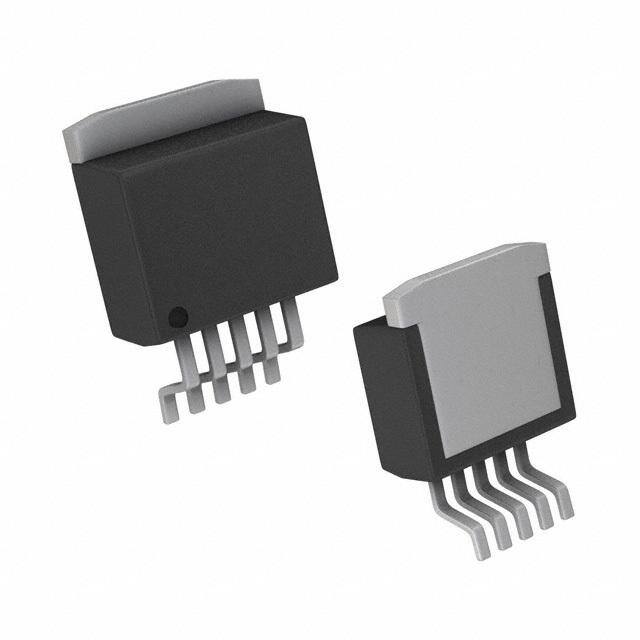
| 产品图片 |
|
| rohs | 符合RoHS无铅 / 符合限制有害物质指令(RoHS)规范要求 |
| 产品系列 | 电源管理 IC,低压差稳压器,Texas Instruments TPS7A6050QKTTRQ1自动,AEC-Q100 |
| 数据手册 | |
| 产品型号 | TPS7A6050QKTTRQ1 |
| PCN封装 | |
| PSRR/纹波抑制—典型值 | 60 dB |
| 产品种类 | 低压差稳压器 |
| 供应商器件封装 | DDPAK/TO-263-5 |
| 其它名称 | 296-27206-1 |
| 包装 | 剪切带 (CT) |
| 商标 | Texas Instruments |
| 回动电压—最大值 | 500 mV |
| 安装类型 | 表面贴装 |
| 安装风格 | SMD/SMT |
| 封装 | Reel |
| 封装/外壳 | TO-263-6,D²Pak(5 引线+接片),TO-263BA |
| 封装/箱体 | TO-263-5 |
| 工作温度 | -40°C ~ 150°C |
| 工厂包装数量 | 500 |
| 最大功率耗散 | 3.63 W |
| 最大工作温度 | + 125 C |
| 最大输入电压 | 40 V |
| 最小工作温度 | - 40 C |
| 最小输入电压 | 5.3 V |
| 标准包装 | 1 |
| 电压-跌落(典型值) | - |
| 电压-输入 | 5.3 V ~ 40 V |
| 电压-输出 | 5V |
| 电流-输出 | 300mA |
| 电流-限制(最小值) | 350mA |
| 稳压器拓扑 | 正,固定式 |
| 稳压器数 | 1 |
| 系列 | TPS7A6050-Q1 |
| 线路调整率 | 15 mV |
| 负载调节 | 25 mV |
| 输出电压 | 5 V |
| 输出电流 | 300 mA |
| 输出端数量 | 1 Output |
| 输出类型 | Fixed |


PDF Datasheet 数据手册内容提取
Product Order Technical Tools & Support & Folder Now Documents Software Community TPS7A60-Q1,TPS7A61-Q1 SLVSA62J–MARCH2010–REVISEDMARCH2020 TPS7A6x-Q1 300-mA, 40-V Low-Dropout Regulator With 25-µA Quiescent Current 1 Features 3 Description • AEC-Q100qualifiedforautomotiveapplications: The TPS7A60-Q1 and TPS7A61-Q1 comprise a 1 family of low-dropout linear voltage regulators – Temperaturegrade1: –40°Cto125°C,T A designed for low power consumption and quiescent – JunctionTemperature: –40°Cto150°C,T current less than 25 µA in light-load applications. J • Lowdropoutvoltage: These devices feature integrated overcurrent protection and are designed to achieve stable – 300mVatI =150mA OUT operation even with low-ESR ceramic capacitors. • 7-Vto40-Vwideinputvoltagerangewithupto Power-on-reset delay is implemented during device 45-Vtransients start-up to indicate that the output voltage is stable • 300-mAmaximumoutputcurrent and in regulation. The power-on-reset delay is fixed (250 µs typical), and can also be programmed by an • Ultralowquiescentcurrent: external capacitor. A low-voltage tracking feature – IQUIESCENT =25 µA(typical)atlightloads allows for a smaller input capacitor and can possibly – I < 2µAwhenENABLE=low eliminate the need of using a boost converter during SLEEP cold-crank conditions. Because of these features, • 3.3-Vand5-Vfixedoutputvoltage these devices are well-suited in power supplies for • Low-ESRceramicoutputstabilitycapacitor variousautomotiveapplications. • Integratedpower-onreset: – Programmabledelay DeviceInformation(1) – Open-drainresetoutput PARTNUMBER PACKAGE BODYSIZE(NOM) TO-263(5) 10.16mm×9.15mm • Integratedfaultprotection: TPS7A6033-Q1 TO-252(5) 6.10mm×6.60mm – Short-circuitandovercurrentprotection TO-263(5) 10.16mm×9.15mm – Thermalshutdown TPS7A6050-Q1 TO-252(5) 6.10mm×6.60mm • Low-input-voltagetracking TPS7A6133-Q1 TO-252(5) 6.10mm×6.60mm • Thermallyenhancedpowerpackages: TPS7A6150-Q1 TO-252(5) 6.10mm×6.60mm – 5-pinTO-263(KTT,D2PAK) (1) For all available packages, see the orderable addendum at – 5-pinTO-252(KVU,DPAK) theendofthedatasheet. 2 Applications • Automotiveheadunits • Automotivecenterinformationdisplays • Hybridinstrumentclusters ProgrammableResetDelayOption EnableOption TPS7A60-Q1 TPS7A61-Q1 VIN VIN VOUT VOUT VIN VIN VOUT VOUT C OUT C C C OUT IN IN RDELAY RRST VIN ENABLE RRST C DLY GND nRST RESET GND nRST RESET 1 An IMPORTANT NOTICE at the end of this data sheet addresses availability, warranty, changes, use in safety-critical applications, intellectualpropertymattersandotherimportantdisclaimers.PRODUCTIONDATA.
TPS7A60-Q1,TPS7A61-Q1 SLVSA62J–MARCH2010–REVISEDMARCH2020 www.ti.com Table of Contents 1 Features.................................................................. 1 8.3 FeatureDescription.................................................13 2 Applications........................................................... 1 8.4 DeviceFunctionalModes........................................17 3 Description............................................................. 1 9 ApplicationandImplementation........................ 18 4 RevisionHistory..................................................... 2 9.1 ApplicationInformation............................................18 9.2 TypicalApplications................................................18 5 DeviceComparisonTable..................................... 4 10 PowerSupplyRecommendations..................... 22 6 PinConfigurationandFunctions......................... 5 11 Layout................................................................... 22 7 Specifications......................................................... 6 11.1 LayoutGuidelines.................................................22 7.1 AbsoluteMaximumRatings......................................6 11.2 LayoutExamples...................................................25 7.2 ESDRatings..............................................................6 12 DeviceandDocumentationSupport................. 27 7.3 RecommendedOperatingConditions.......................6 7.4 ThermalInformation..................................................7 12.1 RelatedLinks........................................................27 7.5 ElectricalCharacteristics...........................................7 12.2 ReceivingNotificationofDocumentationUpdates27 7.6 SwitchingCharacteristics..........................................8 12.3 CommunityResources..........................................27 7.7 TypicalCharacteristics..............................................9 12.4 Trademarks...........................................................27 12.5 ElectrostaticDischargeCaution............................27 8 DetailedDescription............................................ 12 12.6 Glossary................................................................27 8.1 Overview.................................................................12 13 Mechanical,Packaging,andOrderable 8.2 FunctionalBlockDiagrams.....................................12 Information........................................................... 27 4 Revision History NOTE:Pagenumbersforpreviousrevisionsmaydifferfrompagenumbersinthecurrentversion. ChangesfromRevisionI(May2018)toRevisionJ Page • ChangedAEC-Q100Featuresbulletstoconformtonewstandard ...................................................................................... 1 • Changedinputvoltagerangefrom11Vto7Vthroughoutdocument................................................................................... 1 • ChangedApplicationssection ............................................................................................................................................... 1 • AddedfootnotetoV rowinRecommendedOperatingConditionstable ............................................................................ 6 IN • AddedfootnotetoV rowinElectricalCharacteristicstable ................................................................................................ 7 IN ChangesfromRevisionH(March2016)toRevisionI Page • ChangeddevicenamesfromTPS7A6033-Q1,TPS7A6050-Q1,TPS7A6133-Q1,andTPS7A6150-Q1toTPS7A60- Q1andTPS7A61-Q1............................................................................................................................................................. 1 • Changed4Vto11VinfourthFeaturesbullet ...................................................................................................................... 1 • ChangedV minimumspecificationfrom4Vto11VinRecommendedOperatingConditionstable.................................. 6 IN • ChangedV andV parameterstobeseparaterows,changedV descriptiontoEnablepinvoltage ................6 IN ENABLE ENABLE • ChangedV parameter:condensedtestconditionstoonerowandchangedminimumspecificationfrom5.3Vto11V...7 IN • Changed4V(3.3-Vversion)or5.3V(5-Vversion)to11VinRegulationModesection .................................................. 17 • ChangedInputvoltagerangeparameterexamplevalueinTPS7A60-Q1DesignParameterstable.................................. 18 • ChangedInputvoltagerangeparameterexamplevalueinTPS7A61-Q1DesignParameterstable ................................. 20 ChangesfromRevisionG(April2012)toRevisionH Page • AddednewbulletstotopofFeatureslist............................................................................................................................... 1 • Appended"-Q1"tothepartnumberinnumerouslocationsthroughoutthedatasheet......................................................... 1 • AddedESDRatingtable,SwitchingCharacteristicstableFeatureDescriptionsection,DeviceFunctionalModes, ApplicationandImplementationsection,PowerSupplyRecommendationssection,Layoutsection,Deviceand DocumentationSupportsection,andMechanical,Packaging,andOrderableInformationsection....................................... 1 • AddedMINvaluesforVIN,RDELAY,andVOUTinAbsoluteMaximumRatingstable......................................................... 6 2 SubmitDocumentationFeedback Copyright©2010–2020,TexasInstrumentsIncorporated ProductFolderLinks:TPS7A60-Q1 TPS7A61-Q1
TPS7A60-Q1,TPS7A61-Q1 www.ti.com SLVSA62J–MARCH2010–REVISEDMARCH2020 • DeletedtwographsfromtheTypicalCharacteristicssection................................................................................................. 9 • UpdatedTypicalApplicationSchematicfortheTPS7A61xx-Q1Deviceimage. ................................................................. 20 Copyright©2010–2020,TexasInstrumentsIncorporated SubmitDocumentationFeedback 3 ProductFolderLinks:TPS7A60-Q1 TPS7A61-Q1
TPS7A60-Q1,TPS7A61-Q1 SLVSA62J–MARCH2010–REVISEDMARCH2020 www.ti.com 5 Device Comparison Table PROGRAMMABLERESET PARTNUMBER OUTPUTVOLTAGE ENABLE RESET DELAY No Yes Yes TPS7A6033-Q1 3.3V No Yes Yes No Yes Yes TPS7A6050-Q1 5V No Yes Yes TPS7A6133-Q1 3.3V Yes Yes No TPS7A6150-Q1 5V Yes Yes No 4 SubmitDocumentationFeedback Copyright©2010–2020,TexasInstrumentsIncorporated ProductFolderLinks:TPS7A60-Q1 TPS7A61-Q1
TPS7A60-Q1,TPS7A61-Q1 www.ti.com SLVSA62J–MARCH2010–REVISEDMARCH2020 6 Pin Configuration and Functions KTTPackage KVUPackage 5-PinTO-263WithExposedThermalPad 5-PinTO-252WithExposedThermalPad TopView TopView Thermal Thermal Pad Pad 1 2 3 4 5 1 2 3 4 5 N T D Y T N T D Y T VI nRS GN RDELA VOU VI nRS GN RDELA VOU E, E, L L B B A A N N E E PinFunctions PIN TYPE DESCRIPTION NAME NO. Enablepin(forTPS7A61-Q1only):Thisisahigh-voltage-tolerantinputpinwithaninternalpulldown.Ahigh ENABLE 4 I inputtothispinactivatesthedeviceandturnstheregulatorON.ThisinputcanbeconnectedtotheVINpin forself-biasapplications.Ifthispinisnotconnected,thedevicestaysdisabled. GND 3 I/O Groundpin:Thisisthesignal-groundpinoftheIC. nRST 2 O Resetpin:ThisisanoutputpinwithanexternalpullupresistorconnectedtotheVOUTpin. Resetdelaytimerpin(forTPS7A60-Q1only):Thispinisusedtoprogramtheresetdelaytimerusingan RDELAY 4 O externalcapacitor(C )toground. DLY Inputvoltagepin:Theunregulatedinputvoltageissuppliedtothispin.Abypasscapacitorisconnected VIN 1 I betweentheVINpinandtheGNDpintodampeninputlinetransients. Regulatedoutput-voltagepin:Thisisaregulatedvoltageoutput(V =3.3Vor5V,asapplicable)pinwith OUT VOUT 5 O alimitationonmaximumoutputcurrent.Inordertoachievestableoperationandpreventoscillation,an externaloutputcapacitor(C )withlowESRisconnectedbetweenthispinandtheGNDpin. OUT Copyright©2010–2020,TexasInstrumentsIncorporated SubmitDocumentationFeedback 5 ProductFolderLinks:TPS7A60-Q1 TPS7A61-Q1
TPS7A60-Q1,TPS7A61-Q1 SLVSA62J–MARCH2010–REVISEDMARCH2020 www.ti.com 7 Specifications 7.1 Absolute Maximum Ratings overoperatingfree-airtemperaturerange(unlessotherwisenoted)(1) MIN MAX UNIT Unregulatedinputs(2) VIN,ENABLE –0.3 45 V Regulatedoutput VOUT –0.3 7 V Open-drainresetoutput nRST –0.3 7 V Outputtochargeanexternalcapacitor RDELAY –0.3 7 V Operatingambienttemperature,T –40 150 °C J Storagetemperature,T –65 150 °C stg (1) StressesbeyondthoselistedunderAbsoluteMaximumRatingsmaycausepermanentdamagetothedevice.Thesearestressratings only,whichdonotimplyfunctionaloperationofthedeviceattheseoranyotherconditionsbeyondthoseindicatedunderRecommended OperatingConditions.Exposuretoabsolute-maximum-ratedconditionsforextendedperiodsmayaffectdevicereliability. (2) Absolutemaximumvoltagefordurationlessthan480ms 7.2 ESD Ratings VALUE UNIT TPS7A60-Q1andTPS7A61-Q1DevicesinKVUPackage Human-bodymodel(HBM),perAECQ100-002(1) ±4000 V Electrostaticdischarge V (ESD) Charged-devicemodel(CDM),perAECQ100-011 ±1000 TPS7A60-Q1DeviceinKTTPackage Human-bodymodel(HBM),perAECQ100-002(1) ±4000 V Electrostaticdischarge V (ESD) Charged-devicemodel(CDM),perAECQ100-011 ±1500 (1) AECQ100-002indicatesthatHBMstressingshallbeinaccordancewiththeANSI/ESDA/JEDECJS-001specification. 7.3 Recommended Operating Conditions overoperatingambienttemperaturerange(unlessotherwisenoted) MIN MAX UNIT V Unregulatedinputvoltage 7(1) 40 V IN V Enablepinvoltage(2) 4 40 V ENABLE V ,V Low-voltageoutputrange(3) 0 5.25 V nRST RDELAY I Outputcurrent 0 300 mA OUT T Operatingambienttemperature –40 150 °C A (1) V cangodownto4Vfor130msorlessandremainfunctional.IfV islessthan7Vforlongerthan130ms,thensomedevicescan IN IN turnoffuntiltheinputvoltagerisesabove7V. (2) ApplicablefortheTPS7A61-Q1only. (3) ApplicablefortheTPS7A60-Q1only. 6 SubmitDocumentationFeedback Copyright©2010–2020,TexasInstrumentsIncorporated ProductFolderLinks:TPS7A60-Q1 TPS7A61-Q1
TPS7A60-Q1,TPS7A61-Q1 www.ti.com SLVSA62J–MARCH2010–REVISEDMARCH2020 7.4 Thermal Information TPS7A60-Q1, TPS7A60-Q1 TPS7A61-Q1 THERMALMETRIC(1)(2) UNIT KVU(TO-252) KTT(TO-263) 5PINS 5PINS R Junction-to-ambientthermalresistance 26.9 24.7 °C/W θJA R Junction-to-case(top)thermalresistance 32.2 38.9 °C/W θJC(top) R Junction-to-boardthermalresistance 6.5 7.4 °C/W θJB ψ Junction-to-topcharacterizationparameter 2.5 3.8 °C/W JT ψ Junction-to-boardcharacterizationparameter 6.5 7.4 °C/W JB R Junction-to-case(bottom)thermalresistance 2.8 1.5 °C/W θJC(bot) (1) ThethermaldataisbasedonJEDECstandardhighKprofileJESD51-5.Thecopperpadissolderedtothethermallandpattern.The correctattachmentproceduremustbeincorporated. (2) Formoreinformationabouttraditionalandnewthermalmetrics,seetheSemiconductorandICPackageThermalMetricsapplication report. 7.5 Electrical Characteristics V =14V,T =–40°Cto150°C(unlessotherwisenoted) IN J PARAMETER TESTCONDITIONS MIN TYP MAX UNIT INPUTVOLTAGE(VINPIN) V Inputvoltage Fixed5-Vor3.3-Voutput,I =1mA 7(1) 40 V IN OUT V =8.2Vto18V,V (2)=5V, I Quiescentcurrent IN ENABLE 25 40 µA QUIESCENT I =0.01mAto0.75mA OUT V =8.2Vto18V,V (2)<0.8V, I (2) Sleeporshutdowncurrent IN ENABLE 3 µA SLEEP I =0mA(noload),T =125°C OUT A V Undervoltagelockoutvoltage RampV downuntiloutputisturnedOFF 3.16 V IN-UVLO IN V Power-upvoltage RampV upuntiloutputisturnedON 3.45 V IN(POWERUP) IN ENABLEINPUT(ENABLEPIN) V (2) Logicinputlowlevel 0 0.8 V IL V (2) Logicinputhighlevel 2.5 40 V IH REGULATEDOUTPUTVOLTAGE(VOUTPIN) FixedV value(3.3Vor5Vasapplicable), V Regulatedoutputvoltage OUT –2% 2% OUT I =10mAto300mA,V =V +1Vto16V OUT IN OUT V =6Vto28V,I =10mA,V =5V 15 mV IN OUT OUT ∆V Lineregulation LINE-REG V =6Vto28V,I =10mA,V =3.3V 20 mV IN OUT OUT I =10mAto300mA,V =14V,V =5V 25 mV OUT IN OUT ∆V Loadregulation LOAD-REG I =10mAto300mA,V =14V,V =3.3V 35 mV OUT IN OUT V (3) Dropoutvoltage IOUT=250mA 500 mV DROPOUT (VIN–VOUT) IOUT=150mA 300 mV R Switchresistance VINtoVOUTresistance 2 Ω SW I Outputcurrentlimit V =0V(VOUTpinisshortedtoground) 350 1000 mA CL OUT V =0.5Vpp,I =300mA, IN-RIPPLE OUT 60 frequency=100Hz,V =5VandV =3.3V OUT OUT PSRR Powersupplyripplerejection dB V =0.5Vpp,I =300mA, IN-RIPPLE OUT 30 frequency=150kHz,V =5VandV =3.3V OUT OUT RESET(nRSTPIN) V Resetpulledlow I =5mA 0.4 V OL OL I Leakagecurrent ResetpulledtoVOUTthrough5-kΩresistor 1 µA OH (1) V cangodownto4Vfor130msorlessandremainfunctional.IfV islessthan7Vforlongerthan130ms,thensomedevicescan IN IN turnoffuntiltheinputvoltagerisesabove7V. (2) ApplicablefortheTPS7A61-Q1only. (3) ThistestisdonewithV inregulationandV –V parameterismeasuredwhenV (3.3Vor5V)dropsby100mVatspecified OUT IN OUT OUT loads. Copyright©2010–2020,TexasInstrumentsIncorporated SubmitDocumentationFeedback 7 ProductFolderLinks:TPS7A60-Q1 TPS7A61-Q1
TPS7A60-Q1,TPS7A61-Q1 SLVSA62J–MARCH2010–REVISEDMARCH2020 www.ti.com Electrical Characteristics (continued) V =14V,T =–40°Cto150°C(unlessotherwisenoted) IN J PARAMETER TESTCONDITIONS MIN TYP MAX UNIT V powerupaboveinternallysettolerance, OUT 4.5 4.65 4.77 V =5V OUT V Power-on-resetthreshold V TH(POR) V powerupaboveinternallysettolerance, OUT 3.07 V =3.3V OUT V fallingbelowinternallysettolerance, OUT 4.5 4.65 4.77 V =5V OUT UV Resetthreshold V THRES V fallingbelowinternallysettolerance, OUT 3.07 V =3.3V OUT RESETDELAY(RDELAYPIN) V (4) ThresholdtoreleasenRST VoltageatRDELAYpinisrampedup. 3 3.3 V TH(RDELAY) high I (4) Delaycapacitorcharging 0.75 1 1.25 µA DLY current I (4) Delaycapacitordischarging VoltageatRDELAYpin=1V 5 mA OL current OPERATINGTEMPERATURERANGE Operatingjunction T –40 150 ºC J temperature T Thermalshutdowntrippoint 165 ºC SHUTDOWN T Thermalshutdownhysteresis 10 ºC HYST (4) ApplicablefortheTPS7A60-Q1only. 7.6 Switching Characteristics overoperatingfree-airtemperaturerange(unlessotherwisenoted) PARAMETER TESTCONDITIONS MIN TYP MAX UNIT RESET(nRSTPIN) C =100pF 300 µs DLY t Power-on-resetdelay POR C =100nF 300 ms DLY Internallypresetpower-on- C notconnectedinTPS7A60xxornotavailable t DLY 250 µs POR-PRESET resetdelay inTPS7A61xx,V =5VandV =3.3V OUT OUT t Resetdeglitchtime 5.5 µs DEGLITCH 8 SubmitDocumentationFeedback Copyright©2010–2020,TexasInstrumentsIncorporated ProductFolderLinks:TPS7A60-Q1 TPS7A61-Q1
TPS7A60-Q1,TPS7A61-Q1 www.ti.com SLVSA62J–MARCH2010–REVISEDMARCH2020 7.7 Typical Characteristics 80 55 VIN= 14V VIN=14V 70 TVAO=U 2T5=° C5V, 3.3V 50 VOUT=5V, 3.3V 60 45 IOUT= 250mA A) A) µ 50 µ 40 ( ( ENT 40 ENT 35 C C S S UIE 30 UIE 30 IQ IQ IOUT= 1mA 20 25 10 20 0 15 0.001 0.01 0.1 1 10 100 1000 -50 0 50 100 150 IOUT(mA) TA(°C) Figure1.QuiescentCurrentvsLoadCurrent Figure2.QuiescentCurrentvsAmbientAirTemperature 700 0.4 VOUT= 5V, 3.3V VOUT= 5V 0.35 600 TA= 25°C 0.3 µA)500 (V)0.25 TA= 125°C (NT 400 OUT 0.2 TA= 25°C SCE 300 ROP TA= -40°C UIE IOUT= 100mA VD0.15 Q I200 0.1 100 No Load 0.05 0 0 4 14 24 34 40 0 50 100 150 200 250 300 VIN(V) IOUT(mA) Figure3.QuiescentCurrentvsInputVoltage Figure4.DropoutVoltage (1)vsLoadCurrent 5.1 6 VIN= 14V IOUT= 100mA 5.08 IOUT = 1mA 5 TA= 25°C 5.06 5.04 4 V) 5.02 V) V(OUT 4.958 V(OUT 3 2 4.96 4.94 1 4.92 4.9 0 -50 0 50 100 150 2 3 4 5 6 7 TA(°C) VIN(V) Figure5.OutputVoltagevsAmbientAirTemperature Figure6.OutputVoltagevsInputVoltage (1) Dropoutvoltageismeasuredwhentheoutputvoltagedropsby100mVfromtheregulatedoutputvoltagelevel.(Forexample,dropout voltagefortheTPS7A6050-Q1ismeasuredwhentheoutputvoltagedropsdownto4.9Vfrom5V.) Copyright©2010–2020,TexasInstrumentsIncorporated SubmitDocumentationFeedback 9 ProductFolderLinks:TPS7A60-Q1 TPS7A61-Q1
TPS7A60-Q1,TPS7A61-Q1 SLVSA62J–MARCH2010–REVISEDMARCH2020 www.ti.com Typical Characteristics (continued) 0.12 750 ILOAD= 100mA VIN= 14V 0.1 VOUT = 5V, 3.3V 700 VOUT= 5V, 3.3V 0.08 650 TA= 125°C (A)OUT0.06 TA= 25°C (mA)CL 600 I0.04 TA= -40°C I 550 0.02 500 0 450 0 10 20 30 40 50 -50 0 50 100 150 VIN(V) TA(°C) Figure7.OutputVoltagevsInputVoltage Figure8.OutputCurrentLimitvsAmbientAirTemperature 12 3 mV)111.51 VVI1O0IONUmUT=TAs =1tt e4o5pVV 3 ,f 0r3o0.3mmVA mV) 2.5 IVV8OVOIUN UTtTos= t= 2e1 85p0VV mf,r Ao3m.3V ulation(101.50 ulation ( 1.52 g g e e R 9.5 R d e 1 a n o 9 Li L 0.5 8.5 8 0 -50 0 50 100 150 -50 0 50 100 150 TA(°C) TA(°C) Figure9.LoadRegulationvsAmbientAirTemperature Figure10.LineRegulationvsAmbientAirTemperature 120 120 VIN= 14V VIN = 14V IOUT= 250mA IOUT= 1mA 100 TA= 25°C 100 TA= 25°C COUT= 10µF COUT= 10µF 80 VOUT= 5V, 3.3V 80 VOUT= 5V, 3.3V B) B) d d R( 60 R( 60 R R S S P P 40 40 20 20 0 0 10 100 1k 10k 100k 1M 10 100 1k 10k 100k 1M Frequency (Hz) Frequency (Hz) Figure11.PSRRatHeavyLoadCurrent Figure12.PSRRatLightLoadCurrent 10 SubmitDocumentationFeedback Copyright©2010–2020,TexasInstrumentsIncorporated ProductFolderLinks:TPS7A60-Q1 TPS7A61-Q1
TPS7A60-Q1,TPS7A61-Q1 www.ti.com SLVSA62J–MARCH2010–REVISEDMARCH2020 Typical Characteristics (continued) 10 VIN= 14V COUT= 10µF, 47µF TA= 27°C VOUT= 5V, 3.3V Ω) 1 ( T U O C Stable Operation of Over Entire Region R S E 0.1 0.01 0.01 0.1 1 10 100 300 IOUT(mA) Figure13.ESRStabilityvsLoadCurrent forTPS7A60-Q1andTPS7A61-Q1 Copyright©2010–2020,TexasInstrumentsIncorporated SubmitDocumentationFeedback 11 ProductFolderLinks:TPS7A60-Q1 TPS7A61-Q1
TPS7A60-Q1,TPS7A61-Q1 SLVSA62J–MARCH2010–REVISEDMARCH2020 www.ti.com 8 Detailed Description 8.1 Overview The TPS7A60-Q1 and TPS7A61-Q1 devices comprise a family of monolithic low-dropout linear voltage regulators with integrated reset functionality. These voltage regulators are designed for low power consumption and quiescent current less than 25 µA in light-load applications. These devices are well-suited in power supplies formicroprocessorsandmicrocontrollersbecauseofanintegratedresetdelay,alsocalledpower-on-resetdelay. Thesedevicesareavailableintwofixedoutput-voltage(3.3-Vand5-V)versionsasfollows: • Programmableresetdelayversion(TPS7A60-Q1) • Enableversion(TPS7A61-Q1) 8.2 Functional Block Diagrams V Band Gap VRef1 TemperatureSensor IN Thermal Shutdown VIN C IN UVLO Com.p With Internal Q1 Reference VRef1 + Error Regulator Logic Amp. Control Control V OUT VOUT C OUT Overcurrent Detection R RDELAY RST Voltage Supervisor With Reset Delay C DLY Charge Oscillator Q2 RESET Pump nRST GND Figure14. TPS7A60-Q1FunctionalBlockDiagram 12 SubmitDocumentationFeedback Copyright©2010–2020,TexasInstrumentsIncorporated ProductFolderLinks:TPS7A60-Q1 TPS7A61-Q1
TPS7A60-Q1,TPS7A61-Q1 www.ti.com SLVSA62J–MARCH2010–REVISEDMARCH2020 Functional Block Diagrams (continued) V Band Gap VRef1 TemperatureSensor IN Thermal Shutdown VIN C IN UVLO Com.p With Internal Q1 Reference VRef1 + Error Regulator Logic Amp. Control Control V V OUT ENABLE ENABLE VOUT C OUT Overcurrent Detection R RST Voltage Supervisor With Reset Delay Charge Oscillator Q2 RESET Pump nRST GND Figure15. TPS7A61-Q1FunctionalBlockDiagram 8.3 Feature Description ThefollowingsectiondescribesthefeaturesofTPS7A60-Q1andTPS7A61-Q1voltageregulatorsindetail. 8.3.1 ResetDelayandResetOutput Reset delay is implemented when the device starts up to indicate that output voltage is stable and in regulation, and also when the output recovers from a negative voltage spike due to a load step or a dip in the input voltage for a specified duration. The reset-delay timer is initialized when the voltage at the output (V ) exceeds 93% of OUT the regulated output voltage (3.3 V or 5 V, as applicable). The reset output (nRST) is asserted high after the power-on-reset delay (t ) has elapsed. If the regulated output voltage falls below 93% of the set level, nRST is POR assertedlowafterashortde-glitchtimeofapproximately5.5 µs(typical). For TPS7A60-Q1 devices, the reset-delay time can be programmed by connecting an external capacitor (C ) DLY totheRDELAYpin.ThedelaytimeisgivenbyEquation1: C ´ 3 t = DLY POR 1´10-6 where • t =resetdelaytimeinseconds POR • C =resetdelaycapacitorvalueinfarads,100pFto100nF (1) DLY InTPS7A61xxdevices,thereisnoRDELAYpin,andthereset-delaytimeispresetinternally(250 µstypical). Copyright©2010–2020,TexasInstrumentsIncorporated SubmitDocumentationFeedback 13 ProductFolderLinks:TPS7A60-Q1 TPS7A61-Q1
TPS7A60-Q1,TPS7A61-Q1 SLVSA62J–MARCH2010–REVISEDMARCH2020 www.ti.com Feature Description (continued) During power up, the regulator incorporates a protection scheme to limit the current through the pass element and output capacitor. When the input voltage exceeds a certain threshold (V ) level, the output voltage IN(POWERUP) begins to ramp as shown in Figure 16 and Figure 17. When the output voltage reaches the power-on-reset threshold (V ) level, a constant output current charges an external capacitor (C ) to an internal threshold TH(POR) DLY (V ) voltage level. Then, nRST is asserted high and C is discharged through an internal load. This TH(RDELAY) DLY allows C to charge from approximately 0 V during the next power cycle. If no external capacitor is connected, DLY thedelaytimeispresetinternally.ThisisshowninFigure16. In TPS7A60-Q1 devices, if the C capacitor is not connected to the RDELAY pin, the reset-delay time is set DLY internally.ThisisshowninFigure17. VIN(POWERUP) VIN VTH(POR)=93%of VOUT VOUT VTH(RDELAY) RDELAY Programmable Reset Delay nRST Figure16. PowerUpandReset-DelayFunctionWiththeC CapacitorConnectedtotheRDELAYPin DLY forTPS7A60-Q1 VIN(POWERUP) VIN VTH(POR)=93%of VOUT VOUT VTH(RDELAY) Internal Reset Delay 250µs (typ) nRST Figure17. PowerUpandResetDelayFunctionWiththeC CapacitorNotConnectedorAvailablein DLY TPS7A60-Q1andTPS7A61-Q1,Respectively 14 SubmitDocumentationFeedback Copyright©2010–2020,TexasInstrumentsIncorporated ProductFolderLinks:TPS7A60-Q1 TPS7A61-Q1
TPS7A60-Q1,TPS7A61-Q1 www.ti.com SLVSA62J–MARCH2010–REVISEDMARCH2020 Feature Description (continued) In case of negative transients in the input voltage (V ), the reset signal is asserted low only if the output (V ) IN OUT drops and stays below the reset threshold level (V ) for more than the de-glitch time (t ). This is TH(POR) DEGLITCH showninFigure18. While nRST is low, if the input voltage returns to the nominal operating voltage, the normal power-up sequence is followed. nRST is asserted high, only if the output voltage exceeds the reset-threshold voltage (V ) and TH(POR) thereset-delaytime(t )haselapsed.ThisisshownintheshadedregionofFigure18. POR VIN t < tDEGLITCH t > tDEGLITCH VTH(POR) UVTHRES VOUT VTH(RDELAY) RDELAY tPOR tPOR tDEGLITCH tDEGLITCH nRST Figure18. ConditionsforActivationofReset 8.3.2 ChargePumpOperation Thesedeviceshaveaninternalchargepumpwhich turns on or off depending on the input voltage and the output current. The charge-pump switching circuitry does not cause conducted emissions to exceed required thresholds on the input-voltage line. For a given output current, the charge pump stays on at lower input voltages and turns off at higher input voltages. The charge-pump switching thresholds are hysteretic. Figure 19 and Figure 20 show typical switching thresholds for the charge pump at light (I < approximately 2 mA) and heavy (I > OUT OUT approximately2mA)loads,respectively. e mp Stat ON p State ON m u ge P Hysteresis e Pu Hysteresis r g a r h a COFF Ch OFF 7.8 7.9 9.2 9.6 V (V) V (V) IN IN Figure19.ChargePumpOperationatLightLoads Figure20.ChargePumpOperationatHeavyLoads Copyright©2010–2020,TexasInstrumentsIncorporated SubmitDocumentationFeedback 15 ProductFolderLinks:TPS7A60-Q1 TPS7A61-Q1
TPS7A60-Q1,TPS7A61-Q1 SLVSA62J–MARCH2010–REVISEDMARCH2020 www.ti.com Feature Description (continued) 8.3.3 UndervoltageShutdown These devices have an integrated undervoltage lockout (UVLO) circuit to shut down the output if the input voltage (V ) falls below an internally fixed UVLO threshold level (V ). This ensures that the regulator is not IN IN-UVLO latched into an unknown state during low-input-voltage conditions. The regulator powers up when the input voltageexceedstheV level. IN(POWERUP) 8.3.4 Low-VoltageTracking At low input voltages, the regulator drops out of regulation, and the output voltage tracks the input minus a voltage based on the load current (I ) and switch resistance (R ). This allows for a smaller input capacitor OUT SW andcanpossiblyeliminatetheneedofusingaboostconverterduringcold-crankconditions. 8.3.5 IntegratedFaultProtection These devices feature integrated fault protection to make them ideal for use in automotive applications. In order to keep them in a safe area of operation during certain fault conditions, internal current-limit protection and current-limit foldback are used to limit the maximum output current. This protects them from excessive power dissipation. For example, during a short-circuit condition on the output, current through the pass element is limitedtoI toprotectthedevicefromexcessivepowerdissipation. CL 8.3.6 ThermalShutdown These devices incorporate a thermal shutdown (TSD) circuit as a protection from overheating. For continuous normal operation, the junction temperature should not exceed the TSD trip point. If the junction temperature exceedsthe TSD trip point, the output is turned off. When the junction temperature falls below the TSD trip point, theoutputisturnedonagain.ThisisshowninFigure21. V =24V I =300mA V =5V IN OUT OUT Figure21. ThermalCyclingWaveformfortheTPS7A6150-Q1 16 SubmitDocumentationFeedback Copyright©2010–2020,TexasInstrumentsIncorporated ProductFolderLinks:TPS7A60-Q1 TPS7A61-Q1
TPS7A60-Q1,TPS7A61-Q1 www.ti.com SLVSA62J–MARCH2010–REVISEDMARCH2020 8.4 Device Functional Modes 8.4.1 Low-PowerMode Atlightloadsandhighinputvoltages(V >approximately8V such that charge pump is off), the device operates IN inlow-powermodeandthequiescentcurrentconsumptionisreducedto25µA(typical)asshowninTable1. Table1.TypicalQuiescentCurrentConsumption I CHARGEPUMPON CHARGEPUMPOFF OUT I <approximately2mA(lightload) 250µA 25µA(low-powermode) OUT I >approximately2mA(heavyload) 280µA 70µA OUT 8.4.2 SleepMode(TPS7A61-Q1Only) The enable falling edge is 0.8 V (minimum). The device operates in the sleep mode by holding the ENABLE pin below that voltage, and the quiescent current consumption is reduced to 3 µA (maximum) as shown in Electrical Characteristics. 8.4.3 RegulationMode When the input voltage is above 7 V, with the ENABLE pin pulled higher than 2.5 V, the device operates in regulationmodeandoutputsthenominalvoltage. Copyright©2010–2020,TexasInstrumentsIncorporated SubmitDocumentationFeedback 17 ProductFolderLinks:TPS7A60-Q1 TPS7A61-Q1
TPS7A60-Q1,TPS7A61-Q1 SLVSA62J–MARCH2010–REVISEDMARCH2020 www.ti.com 9 Application and Implementation NOTE Information in the following applications sections is not part of the TI component specification, and TI does not warrant its accuracy or completeness. TI’s customers are responsible for determining suitability of components for their purposes. Customers should validateandtesttheirdesignimplementationtoconfirmsystemfunctionality. 9.1 Application Information The TPS7A60-Q1 and TPS7A61-Q1 devices are 300-mA low-dropout linear regulators designed for up to 40-V V operation with only 25-µA quiescent current at no load. There are specific EVMs designed for these devices IN to enable evaluation of all the functions of the devices. Both the EVM and its user guide are available on the productfolderaswell. 9.2 Typical Applications Figure 22 and Figure 24 show typical application circuits for the TPS7A60-Q1 and TPS7A61-Q1, respectively. One may use different values of external components, depending on the end application. An application may requirealargeroutput capacitor during fast load steps in order to prevent reset from occurring. TI recommends a low-ESRceramiccapacitorwithdielectricoftypeX5RorX7R. 9.2.1 TPS7A60-Q1TypicalApplication TPS7A60-Q1 VIN VIN VOUT VOUT 10 µF 0.1 µF to 10 µF 0.1 µF 22 µF 1 kΩ RDELAY to 100 pF 5 kΩ to 100 nF GND nRST RESET Figure22. TypicalApplicationSchematicfortheTPS7A60-Q1Device 9.2.1.1 DesignRequirements Forthisdesignexample,usetheparameterslistedinTable2. Table2.TPS7A60-Q1DesignParameters DESIGNPARAMETER EXAMPLEVALUE Inputvoltagerange 7Vto40V Outputvoltage 3.3V(forTPS7A6033-Q1)or5V(forTPS7A6050-Q1) Outputcurrentrating 300mA Outputcapacitorrange 10µFto47µF Output-capacitorESRrange 10mΩto10Ω RESET-delaycapacitorrange 100pFto100nF 18 SubmitDocumentationFeedback Copyright©2010–2020,TexasInstrumentsIncorporated ProductFolderLinks:TPS7A60-Q1 TPS7A61-Q1
TPS7A60-Q1,TPS7A61-Q1 www.ti.com SLVSA62J–MARCH2010–REVISEDMARCH2020 9.2.1.2 DetailedDesignProcedure Tobeginthedesignprocess,determinethefollowing: • Inputvoltagerange • Outputvoltage • Outputcurrentrating • Inputcapacitor • Outputcapacitor 9.2.1.2.1 InputCapacitor The device requires an input bypass capacitor, the value of which depends on the application. The typical recommended value for the bypass capacitor is 10 µF. The voltage rating must be greater than the maximum inputvoltage. 9.2.1.2.2 OutputCapacitor The device requires an output capacitor to stabilize the output voltage. TI recommends to selecting a capacitor between10µFand47µFwithESRrangefrom10mΩto10 Ω. 9.2.1.3 ApplicationCurve Figure23. PowerUp(V =5V)With10-msRESETDelay,10ms/div,I =20mA OUT L Copyright©2010–2020,TexasInstrumentsIncorporated SubmitDocumentationFeedback 19 ProductFolderLinks:TPS7A60-Q1 TPS7A61-Q1
TPS7A60-Q1,TPS7A61-Q1 SLVSA62J–MARCH2010–REVISEDMARCH2020 www.ti.com 9.2.2 TPS7A61-Q1TypicalApplication TPS7A61-Q1 VIN VIN VOUT VOUT 10 µF 10 µF 0.1 µF to 0.1 µF 22 µF 1 kΩ VENABLE ENABLE to 5 kΩ GND nRST RESET Figure24. TypicalApplicationSchematicfortheTPS7A61-Q1Device 9.2.2.1 DesignRequirements Forthisdesignexample,usetheparameterslistedinTable3. Table3.TPS7A61-Q1DesignParameters DESIGNPARAMETER EXAMPLEVALUE Inputvoltagerange 7Vto40V Outputvoltage 3.3V(forTPS7A6133-Q1)or5V(forTPS7A6150-Q1) Outputcurrentrating 300mA Outputcapacitorrange 10µFto47µF Output-capacitorESRrange 10mΩto10Ω 9.2.2.2 DetailedDesignProcedure Tobeginthedesignprocess,determinethefollowing: • Inputvoltagerange • Outputvoltage • Outputcurrentrating • Inputcapacitor • Outputcapacitor 20 SubmitDocumentationFeedback Copyright©2010–2020,TexasInstrumentsIncorporated ProductFolderLinks:TPS7A60-Q1 TPS7A61-Q1
TPS7A60-Q1,TPS7A61-Q1 www.ti.com SLVSA62J–MARCH2010–REVISEDMARCH2020 9.2.2.3 ApplicationCurve Figure25. PowerUp(V =5V),10ms/div,I =20mA OUT L Copyright©2010–2020,TexasInstrumentsIncorporated SubmitDocumentationFeedback 21 ProductFolderLinks:TPS7A60-Q1 TPS7A61-Q1
TPS7A60-Q1,TPS7A61-Q1 SLVSA62J–MARCH2010–REVISEDMARCH2020 www.ti.com 10 Power Supply Recommendations Design of the device is for operation from an input voltage supply with a range between 4 V and 40 V. This input supply must be well regulated. If the input supply is located more than a few inches from the TPS7A60-Q1 or TPS7A61-Q1 device, TI recommends adding an electrolytic capacitor with a value of 22 µF and a ceramic bypasscapacitorattheinput. 11 Layout 11.1 Layout Guidelines For the LDO power supply, especially these high voltage and large current ones, layout is an important step. If layout is not carefully designed, the regulator could not deliver enough output current because of the thermal limitation. To improve the thermal performance of the device, and maximize the current output at high ambient temperature, it is recommended to spread the thermal pad as large as possible and put enough thermal vias on thethermalpad.Figure29andFigure30showanexamplelayout. 11.1.1 PowerDissipationandThermalConsiderations PowerdissipatedinthedevicecanbecalculatedusingEquation2. P = I ´ (V -V )+I ´V D OUT IN OUT QUIESCENT IN where • P =continuouspowerdissipation D • I =outputcurrent OUT • V =inputvoltage IN • V =outputvoltage OUT • I =quiescentcurrent (2) QUIESCENT AsI <<I ,therefore,thetermI × V inEquation2canbeignored. QUIESCENT OUT QUIESCENT IN For a device under operation at a given ambient air temperature (T ), the junction temperature (T ) can be A J calculatedusingEquation3. T =T +(R ´P ) J A qJA D where • R =junction-to-ambient-airthermalimpedance (3) θJA 22 SubmitDocumentationFeedback Copyright©2010–2020,TexasInstrumentsIncorporated ProductFolderLinks:TPS7A60-Q1 TPS7A61-Q1
TPS7A60-Q1,TPS7A61-Q1 www.ti.com SLVSA62J–MARCH2010–REVISEDMARCH2020 Layout Guidelines (continued) TheriseinjunctiontemperatureduetopowerdissipationcanbecalculatedusingEquation4. DT =T -T =(R ´P ) J A qJA D (4) For a given maximum junction temperature (T ), the maximum ambient air temperature (T ) at which the J-Max A-Max devicecanoperatecanbecalculatedusingEquation5. T =T -(R ´P ) A-Max J-Max qJA D (5) Example: If I = 100 mA, V = 5 V, V = 14 V, I = 250 µA and R = 30˚C/W, the continuous power OUT OUT IN QUIESCENT θJA dissipated in the device is 0.9 W. The rise in junction temperature due to power dissipation is 27˚C. For a maximum junction temperature of 150˚C, maximum ambient air temperature at which the device can operate is 123˚C. Foradequateheatdissipation,itisrecommendedtosolderthethermalpad(exposedheatsink)to a thermal land pad on the PCB. Doing this provides a heat conduction path from the die to the PCB and reduces overall package thermal resistance. Power derating curves for the TPS7A60-Q1 and TPS7A61-Q1 family of devices in theKTT(TO-263)andKVU(TO-252)packagesareshowninFigure26. 4 3.5 KTT (TO-263)JESD51-5 3 W) KVU (TO-252)JESD51-5 d ( 2.5 e at sip 2 KVU (TO-252)JESD51-3 s Di wer 1.5 KTT (TO-263)JESD51-3 o P 1 0.5 0 0 25 50 75 100 125 150 AmbientAir Temperature (°C) Figure26. PowerDeratingCurves For optimum thermal performance, TI recommends to use a high-K PCB with thermal vias between the ground plane and solder pad or thermal land pad. This is shown in Figure 27 (a) and (b). Further, the heat-spreading capabilities of a PCB can be considerably improved by using a thicker ground plane and a thermal land pad with alargersurfacearea. Copyright©2010–2020,TexasInstrumentsIncorporated SubmitDocumentationFeedback 23 ProductFolderLinks:TPS7A60-Q1 TPS7A61-Q1
TPS7A60-Q1,TPS7A61-Q1 SLVSA62J–MARCH2010–REVISEDMARCH2020 www.ti.com Layout Guidelines (continued) ExposedTab Thermal Via Thermal Land Pad PCB Ground Plane (a) Before soldering (b)After soldering Figure27. UsingMultilayerPCBandThermalViasForAdequateHeatDissipation Keeping other factors constant, surface area of the thermal land pad contributes to heat dissipation only to a certain extent. Figure 28 shows the variation of R with surface area of the thermal land pad (soldered to the θJA exposedpad)forKTTandKVUpackages. 55 50 W) 45 C/ KVU (TO-252) (JESD51-3) (° A J Rq 40 KTT (TO-263) (JESD51-3) 35 30 0 200 400 600 800 1000 Thermal PadArea (sq. mm) Figure28. R vsThermalPadArea θJA 24 SubmitDocumentationFeedback Copyright©2010–2020,TexasInstrumentsIncorporated ProductFolderLinks:TPS7A60-Q1 TPS7A61-Q1
TPS7A60-Q1,TPS7A61-Q1 www.ti.com SLVSA62J–MARCH2010–REVISEDMARCH2020 11.2 Layout Examples 1 2 3 4 5 RDELAY/ VIN nRST ENABLE GND VOUT Figure29. LayoutRecommendationfor5-PinKTTPackage Copyright©2010–2020,TexasInstrumentsIncorporated SubmitDocumentationFeedback 25 ProductFolderLinks:TPS7A60-Q1 TPS7A61-Q1
TPS7A60-Q1,TPS7A61-Q1 SLVSA62J–MARCH2010–REVISEDMARCH2020 www.ti.com Layout Examples (continued) 1 2 3 4 5 RDELAY/ VIN nRST GND ENABLE VOUT Figure30. LayoutRecommendationfor5-pinKVUpackage 26 SubmitDocumentationFeedback Copyright©2010–2020,TexasInstrumentsIncorporated ProductFolderLinks:TPS7A60-Q1 TPS7A61-Q1
TPS7A60-Q1,TPS7A61-Q1 www.ti.com SLVSA62J–MARCH2010–REVISEDMARCH2020 12 Device and Documentation Support 12.1 Related Links The table below lists quick access links. Categories include technical documents, support and community resources,toolsandsoftware,andquickaccesstoordernow. Table4.RelatedLinks TECHNICAL TOOLS& SUPPORT& PARTS PRODUCTFOLDER ORDERNOW DOCUMENTS SOFTWARE COMMUNITY TPS7A60-Q1 Clickhere Clickhere Clickhere Clickhere Clickhere TPS7A61-Q1 Clickhere Clickhere Clickhere Clickhere Clickhere 12.2 Receiving Notification of Documentation Updates To receive notification of documentation updates, navigate to the device product folder on ti.com. In the upper right corner, click on Alert me to register and receive a weekly digest of any product information that has changed.Forchangedetails,reviewtherevisionhistoryincludedinanyreviseddocument. 12.3 Community Resources TI E2E™ support forums are an engineer's go-to source for fast, verified answers and design help — straight fromtheexperts.Searchexistinganswersoraskyourownquestiontogetthequickdesignhelpyouneed. Linked content is provided "AS IS" by the respective contributors. They do not constitute TI specifications and do notnecessarilyreflectTI'sviews;seeTI'sTermsofUse. 12.4 Trademarks E2EisatrademarkofTexasInstruments. Allothertrademarksarethepropertyoftheirrespectiveowners. 12.5 Electrostatic Discharge Caution This integrated circuit can be damaged by ESD. Texas Instruments recommends that all integrated circuits be handled with appropriateprecautions.Failuretoobserveproperhandlingandinstallationprocedurescancausedamage. ESDdamagecanrangefromsubtleperformancedegradationtocompletedevicefailure.Precisionintegratedcircuitsmaybemore susceptibletodamagebecauseverysmallparametricchangescouldcausethedevicenottomeetitspublishedspecifications. 12.6 Glossary SLYZ022—TIGlossary. Thisglossarylistsandexplainsterms,acronyms,anddefinitions. 13 Mechanical, Packaging, and Orderable Information The following pages include mechanical, packaging, and orderable information. This information is the most- current data available for the designated devices. This data is subject to change without notice and without revisionofthisdocument.Forbrowser-basedversionsofthisdatasheet,seetheleft-handnavigationpane. Copyright©2010–2020,TexasInstrumentsIncorporated SubmitDocumentationFeedback 27 ProductFolderLinks:TPS7A60-Q1 TPS7A61-Q1
PACKAGE OPTION ADDENDUM www.ti.com 6-Feb-2020 PACKAGING INFORMATION Orderable Device Status Package Type Package Pins Package Eco Plan Lead/Ball Finish MSL Peak Temp Op Temp (°C) Device Marking Samples (1) Drawing Qty (2) (6) (3) (4/5) TPS7A6033QKTTRQ1 ACTIVE DDPAK/ KTT 5 500 Green (RoHS SN Level-3-245C-168 HR -40 to 125 7A6033Q1 TO-263 & no Sb/Br) TPS7A6033QKVURQ1 ACTIVE TO-252 KVU 5 2500 Green (RoHS SN Level-3-260C-168 HR -40 to 125 7A6033Q1 & no Sb/Br) TPS7A6050QKTTRQ1 ACTIVE DDPAK/ KTT 5 500 Green (RoHS SN Level-3-245C-168 HR -40 to 125 7A6050Q1 TO-263 & no Sb/Br) TPS7A6050QKVURQ1 ACTIVE TO-252 KVU 5 2500 Green (RoHS SN Level-3-260C-168 HR -40 to 125 7A6050Q1 & no Sb/Br) TPS7A6133QKVURQ1 ACTIVE TO-252 KVU 5 2500 Green (RoHS SN Level-3-260C-168 HR -40 to 125 7A6133Q1 & no Sb/Br) TPS7A6150QKVURQ1 ACTIVE TO-252 KVU 5 2500 Green (RoHS SN Level-3-260C-168 HR -40 to 125 7A6150Q1 & no Sb/Br) (1) The marketing status values are defined as follows: ACTIVE: Product device recommended for new designs. LIFEBUY: TI has announced that the device will be discontinued, and a lifetime-buy period is in effect. NRND: Not recommended for new designs. Device is in production to support existing customers, but TI does not recommend using this part in a new design. PREVIEW: Device has been announced but is not in production. Samples may or may not be available. OBSOLETE: TI has discontinued the production of the device. (2) RoHS: TI defines "RoHS" to mean semiconductor products that are compliant with the current EU RoHS requirements for all 10 RoHS substances, including the requirement that RoHS substance do not exceed 0.1% by weight in homogeneous materials. Where designed to be soldered at high temperatures, "RoHS" products are suitable for use in specified lead-free processes. TI may reference these types of products as "Pb-Free". RoHS Exempt: TI defines "RoHS Exempt" to mean products that contain lead but are compliant with EU RoHS pursuant to a specific EU RoHS exemption. Green: TI defines "Green" to mean the content of Chlorine (Cl) and Bromine (Br) based flame retardants meet JS709B low halogen requirements of <=1000ppm threshold. Antimony trioxide based flame retardants must also meet the <=1000ppm threshold requirement. (3) MSL, Peak Temp. - The Moisture Sensitivity Level rating according to the JEDEC industry standard classifications, and peak solder temperature. (4) There may be additional marking, which relates to the logo, the lot trace code information, or the environmental category on the device. (5) Multiple Device Markings will be inside parentheses. Only one Device Marking contained in parentheses and separated by a "~" will appear on a device. If a line is indented then it is a continuation of the previous line and the two combined represent the entire Device Marking for that device. Addendum-Page 1
PACKAGE OPTION ADDENDUM www.ti.com 6-Feb-2020 (6) Lead/Ball Finish - Orderable Devices may have multiple material finish options. Finish options are separated by a vertical ruled line. Lead/Ball Finish values may wrap to two lines if the finish value exceeds the maximum column width. Important Information and Disclaimer:The information provided on this page represents TI's knowledge and belief as of the date that it is provided. TI bases its knowledge and belief on information provided by third parties, and makes no representation or warranty as to the accuracy of such information. Efforts are underway to better integrate information from third parties. TI has taken and continues to take reasonable steps to provide representative and accurate information but may not have conducted destructive testing or chemical analysis on incoming materials and chemicals. TI and TI suppliers consider certain information to be proprietary, and thus CAS numbers and other limited information may not be available for release. In no event shall TI's liability arising out of such information exceed the total purchase price of the TI part(s) at issue in this document sold by TI to Customer on an annual basis. Addendum-Page 2
PACKAGE MATERIALS INFORMATION www.ti.com 24-Apr-2020 TAPE AND REEL INFORMATION *Alldimensionsarenominal Device Package Package Pins SPQ Reel Reel A0 B0 K0 P1 W Pin1 Type Drawing Diameter Width (mm) (mm) (mm) (mm) (mm) Quadrant (mm) W1(mm) TPS7A6033QKTTRQ1 DDPAK/ KTT 5 500 330.0 24.4 10.6 15.8 4.9 16.0 24.0 Q2 TO-263 TPS7A6033QKVURQ1 TO-252 KVU 5 2500 330.0 16.4 6.9 10.5 2.7 8.0 16.0 Q2 TPS7A6050QKTTRQ1 DDPAK/ KTT 5 500 330.0 24.4 10.6 15.8 4.9 16.0 24.0 Q2 TO-263 TPS7A6050QKVURQ1 TO-252 KVU 5 2500 330.0 16.4 6.9 10.5 2.7 8.0 16.0 Q2 TPS7A6133QKVURQ1 TO-252 KVU 5 2500 330.0 16.4 6.9 10.5 2.7 8.0 16.0 Q2 TPS7A6150QKVURQ1 TO-252 KVU 5 2500 330.0 16.4 6.9 10.5 2.7 8.0 16.0 Q2 PackMaterials-Page1
PACKAGE MATERIALS INFORMATION www.ti.com 24-Apr-2020 *Alldimensionsarenominal Device PackageType PackageDrawing Pins SPQ Length(mm) Width(mm) Height(mm) TPS7A6033QKTTRQ1 DDPAK/TO-263 KTT 5 500 340.0 340.0 38.0 TPS7A6033QKVURQ1 TO-252 KVU 5 2500 340.0 340.0 38.0 TPS7A6050QKTTRQ1 DDPAK/TO-263 KTT 5 500 340.0 340.0 38.0 TPS7A6050QKVURQ1 TO-252 KVU 5 2500 340.0 340.0 38.0 TPS7A6133QKVURQ1 TO-252 KVU 5 2500 340.0 340.0 38.0 TPS7A6150QKVURQ1 TO-252 KVU 5 2500 340.0 340.0 38.0 PackMaterials-Page2
None
None
None
None
IMPORTANTNOTICEANDDISCLAIMER TI PROVIDES TECHNICAL AND RELIABILITY DATA (INCLUDING DATASHEETS), DESIGN RESOURCES (INCLUDING REFERENCE DESIGNS), APPLICATION OR OTHER DESIGN ADVICE, WEB TOOLS, SAFETY INFORMATION, AND OTHER RESOURCES “AS IS” AND WITH ALL FAULTS, AND DISCLAIMS ALL WARRANTIES, EXPRESS AND IMPLIED, INCLUDING WITHOUT LIMITATION ANY IMPLIED WARRANTIES OF MERCHANTABILITY, FITNESS FOR A PARTICULAR PURPOSE OR NON-INFRINGEMENT OF THIRD PARTY INTELLECTUAL PROPERTY RIGHTS. These resources are intended for skilled developers designing with TI products. You are solely responsible for (1) selecting the appropriate TI products for your application, (2) designing, validating and testing your application, and (3) ensuring your application meets applicable standards, and any other safety, security, or other requirements. These resources are subject to change without notice. TI grants you permission to use these resources only for development of an application that uses the TI products described in the resource. Other reproduction and display of these resources is prohibited. No license is granted to any other TI intellectual property right or to any third party intellectual property right. TI disclaims responsibility for, and you will fully indemnify TI and its representatives against, any claims, damages, costs, losses, and liabilities arising out of your use of these resources. TI’s products are provided subject to TI’s Terms of Sale (www.ti.com/legal/termsofsale.html) or other applicable terms available either on ti.com or provided in conjunction with such TI products. TI’s provision of these resources does not expand or otherwise alter TI’s applicable warranties or warranty disclaimers for TI products. Mailing Address: Texas Instruments, Post Office Box 655303, Dallas, Texas 75265 Copyright © 2020, Texas Instruments Incorporated