ICGOO在线商城 > 集成电路(IC) > PMIC - 稳压器 - 线性 > L6932D1.2TR
 Datasheet下载
- 型号: L6932D1.2TR
- 制造商: STMicroelectronics
- 库位|库存: xxxx|xxxx
- 要求:
| 数量阶梯 | 香港交货 | 国内含税 |
| +xxxx | $xxxx | ¥xxxx |
查看当月历史价格
查看今年历史价格
L6932D1.2TR产品简介:
ICGOO电子元器件商城为您提供L6932D1.2TR由STMicroelectronics设计生产,在icgoo商城现货销售,并且可以通过原厂、代理商等渠道进行代购。 L6932D1.2TR价格参考¥13.29-¥13.29。STMicroelectronicsL6932D1.2TR封装/规格:PMIC - 稳压器 - 线性, Linear Voltage Regulator IC Positive Adjustable 1 Output 1.2 V ~ 5 V 2A 8-SO。您可以下载L6932D1.2TR参考资料、Datasheet数据手册功能说明书,资料中有L6932D1.2TR 详细功能的应用电路图电压和使用方法及教程。
L6932D1.2TR 是由 STMicroelectronics(意法半导体)生产的一款线性稳压器,属于 PMIC(电源管理集成电路)系列。它是一款低功耗、低压差线性稳压器(LDO),输出电压为 1.2V,适用于多种便携式设备和低功耗应用场景。

 应用场景:
1. 消费电子设备
   - 智能手机和平板电脑:为内部低功耗组件(如传感器、MCU 和射频模块)提供稳定的 1.2V 电源。
   - 可穿戴设备(如智能手表、健身追踪器):由于其低功耗特性,非常适合电池供电的可穿戴设备。
   - 音频设备:为耳机放大器或音频处理器提供干净的电源,减少噪声干扰。

2. 物联网 (IoT) 设备
   - 无线传感器节点:为微控制器和传感器供电,确保长时间运行并降低功耗。
   - 智能家居设备:如温控器、智能门锁等,需要稳定且高效的电源管理。

3. 工业应用
   - 工业自动化:为嵌入式系统中的 MCU、FPGA 或其他低功耗芯片供电。
   - 数据采集模块:为 ADC、DAC 等模拟电路提供低噪声电源,提高测量精度。

4. 医疗电子设备
   - 便携式医疗设备:如血糖仪、脉搏血氧仪等,要求高精度和低功耗的电源管理。
   - 远程健康监测设备:为低功耗蓝牙模块和传感器供电。

5. 汽车电子
   - 车载信息娱乐系统:为辅助芯片供电,确保系统的稳定性和可靠性。
   - 传感器模块:为车内温度、压力等传感器提供稳定的电源。

 特点与优势:
- 低静态电流:有助于延长电池寿命,适合电池供电设备。
- 低压差:在输入电压接近输出电压时仍能高效工作,进一步节省电能。
- 高纹波抑制比 (PSRR):有效降低输出电压的噪声,适合对电源质量要求较高的应用。
- 小型封装:采用 SOT23 封装,节省 PCB 空间,便于设计紧凑型产品。

综上所述,L6932D1.2TR 的应用场景广泛,尤其适合需要低功耗、小尺寸和高稳定性电源解决方案的设备。
| 参数 | 数值 |
| 产品目录 | 集成电路 (IC)半导体 |
| 描述 | IC REG LDO 1.2V 2A 8SO低压差稳压器 1.2V 2A Ultra LDO |
| 产品分类 | |
| 品牌 | STMicroelectronics |
| 产品手册 | |
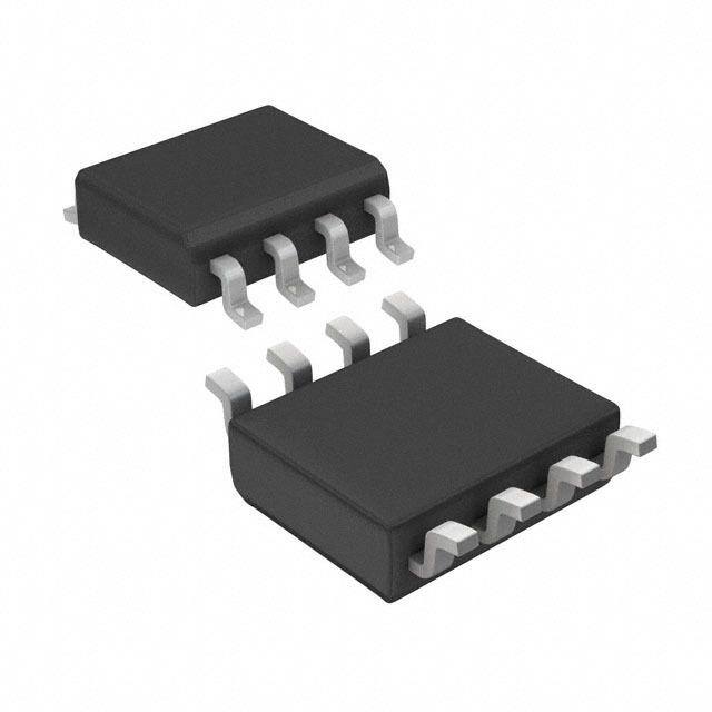
| 产品图片 |
|
| rohs | 符合RoHS无铅 / 符合限制有害物质指令(RoHS)规范要求 |
| 产品系列 | 电源管理 IC,低压差稳压器,STMicroelectronics L6932D1.2TR- |
| 数据手册 | |
| 产品型号 | L6932D1.2TR |
| 产品目录页面 | |
| 产品种类 | 低压差稳压器 |
| 供应商器件封装 | 8-SO |
| 其它名称 | 497-5724-2 |
| 其它有关文件 | http://www.st.com/web/catalog/sense_power/FM142/CL1456/SC277/PF75828?referrer=70071840 |
| 包装 | 带卷 (TR) |
| 商标 | STMicroelectronics |
| 回动电压—最大值 | 1.5 V |
| 安装类型 | 表面贴装 |
| 安装风格 | SMD/SMT |
| 封装 | Reel |
| 封装/外壳 | 8-SOIC(0.154",3.90mm 宽) |
| 封装/箱体 | SO-8 |
| 工作温度 | -25°C ~ 125°C |
| 工厂包装数量 | 2500 |
| 最大工作温度 | + 150 C |
| 最大输入电压 | 14 V |
| 最小输入电压 | + 2 V |
| 标准包装 | 2,500 |
| 电压-跌落(典型值) | - |
| 电压-输入 | 2 V ~ 14 V |
| 电压-输出 | 1.2V |
| 电压调节准确度 | 1 % |
| 电流-输出 | 2A |
| 电流-限制(最小值) | 2.3A |
| 稳压器拓扑 | 正,固定式 |
| 稳压器数 | 1 |
| 系列 | L6932 |
| 线路调整率 | 5 mV |
| 负载调节 | 15 mV |
| 输入偏压电流—最大 | 0.2 mA |
| 输出电压 | 1.2 V to 5 V |
| 输出电流 | 2.5 A |
| 输出端数量 | 1 Output |
| 输出类型 | Adjustable |


- 商务部:美国ITC正式对集成电路等产品启动337调查
- 曝三星4nm工艺存在良率问题 高通将骁龙8 Gen1或转产台积电
- 太阳诱电将投资9.5亿元在常州建新厂生产MLCC 预计2023年完工
- 英特尔发布欧洲新工厂建设计划 深化IDM 2.0 战略
- 台积电先进制程称霸业界 有大客户加持明年业绩稳了
- 达到5530亿美元!SIA预计今年全球半导体销售额将创下新高
- 英特尔拟将自动驾驶子公司Mobileye上市 估值或超500亿美元
- 三星加码芯片和SET,合并消费电子和移动部门,撤换高东真等 CEO
- 三星电子宣布重大人事变动 还合并消费电子和移动部门
- 海关总署:前11个月进口集成电路产品价值2.52万亿元 增长14.8%


PDF Datasheet 数据手册内容提取
L6932 HIGH PERFORMANCE 2A ULDO LINEAR REGULATOR ■ 2V TO 14V INPUT VOLTAGE RANGE ■ 200mΩ Rdson MAX. ■ 200µA QUIESCENT CURRENT AT ANY LOAD ■ EXCELLENT LOAD AND LINE REGULATION ■ 1.5V, 1.8V AND 2.5V FIXED VOLTAGE SO-8 (4+4) ■ ADJUSTABLE FROM 1.2V TO 5V (L6932D1.2) ■ 1% VOLTAGE REGULATION ACCURACY ORDERING NUMBERS: ■ SHORT CIRCUIT PROTECTION L6932D1.2 (SO-8) L6932D1.2TR (T&R) L6932D1.5 (SO-8) L6932D1.5TR (T&R) ■ THERMAL SHUT DOWN L6932D1.8 (SO-8) L6932D1.8TR (T&R) ■ SO-8 (4+4) PACKAGE L6932D2.5 (SO-8) L6932D2.5TR (T&R) APPLICATIONS Mosfet, can be usefull for the DC-DC conversion ■ MOTHERBOARDS between 2.5V and 1.5V at 2A in portable applica- tions reducing the power dissipation. ■ MOBILE PC L6932 is available in 1.5V, 1.8V, 2.5V and adj ver- ■ HAND-HELD INSTRUMENTS sion from 1.2V and ensure a voltage regulation ac- ■ PCMCIA CARDS curacy of 1%. ■ PROCESSORS I/O The current limit is fixed at 2.5A to control the cur- rent in short circuit condition within ±8%. The cur- ■ CHIPSET AND RAM SUPPLY rent is sensed in the power mos in order to limit the power dissipation. DESCRIPTION The device is also provided of a thermal shut down The L6932 Ultra Low Drop Output linear regulator that limits the internal temperature at 150°C with operates from 2V to 14V and is able to support 2A. an histeresys of 20°C. L6932 provides the Enable Designed with an internal 50mΩ N-channel and the Power good functions. TYPICAL OPERATING CIRCUIT VIN IN 2 3 OUT VOUT 2V to 14V 1.5V-1.8V-2.5V L6932D C1 4 PGOOD C2 5,6,7,8 1 GND EN VIN IN 2 4 OUT VOUT 2V to 14V 1.2V to 5V L6932D R1 C1 3 ADJ C2 5,6,7,8 1 R2 GND EN Rev. 9 December 2005 1/11
L6932 PIN CONNECTIONS EN 1 8 GND EN 1 8 GND IN 2 7 GND IN 2 7 GND ADJ 3 6 GND OUT 3 6 GND OUT 4 5 GND PGOOD 4 5 GND L6932D1.2 L6932D1.5 L6932D1.8 L6932D2.5 PIN FUNCTION L6232D L6232D N° 1.5/1.8/ Description 1.2 2.5 1 EN Enables the device if connected to Vin and disables the device if forced to gnd. 2 IN Supply voltage. This pin is connected to the drain of the internal N-mos. Connect this pin to a capacitor larger than 10µF. ADJ – Connecting this pin to a voltage divider it is possible to programme the output voltage between 1.2V and 5V. 3 – OUT Regulated output voltage. This pin is connected to the source of the internal N-mos. Connect this pin to a capacitor of 10µF. OUT – Regulated output voltage. This pin is connected to the source of the internal N-mos. Connect this pin to a capacitor of 10µF. 4 – PGOOD Power good output. The pin is open drain and detects the output voltage. It is forced low if the output voltage is lower than 90% of the programmed voltage. 5, 6, 7, 8 GND Ground pin. ABSOLUTE MAXIMUM RATINGS Symbol Parameter Value Unit Vin VIN and Pgood 14.5 V EN, OUT and ADJ -0.3 to (Vin +0.3) V THERMAL DATA Symbol Parameter Value Unit Rth J-amb Thermal Resistance Junction to Ambient 62 (*) °C/W Tmax Maximum Junction Temperature 150 °C T Storage Temperature Range -65 to 150 °C stg (*) Measured on Demoboard with about 4 cm2 of dissipating area 2 Oz. 2/11
L6932 BLOCK DIAGRAM (Referred to the Fixed Voltage version) IN CHARGE CURRENT PUMP LIMIT VREF DRIVER REFERENCE + VREF=1.25V - ERROR OUT AMPL. THERMAL EN ENABLE SENSOR PG - 0.9 VREF + GND D99IN1100 ELECTRICAL CHARACTERISTCS (T = 25°C, V = 5V unless otherwise specified) j IN (*) Specification referred to T from -25°C to 125°C. j Symbol Parameter Test Condition Min. Typ. Max. Unit Vin Operating Supply Voltage 2 14 V Vo Output voltage L6932D1.2 Io = 0.1A; Vin = 3.3V 1.188 1.2 1.212 V Output voltage L6932D1.5 Io = 0.1A; Vin = 3.3V 1.485 1.5 1.515 V Output voltage L6932D1.8 Io = 0.1A; Vin = 3.3V 1.782 1.8 1.818 V Output voltage L6932D2.5 Io = 0.1A; Vin = 3.3V 2.475 2.5 2.525 V L6932D1.2 Vin = 2.5V ±10%; Io = 10mA 5 mV Line Regulation Vin = 3.3V ±10%; Io = 10mA 5 mV Vin = 5V ±10%; Io = 10mA 5 mV L6932D1.5 Vin = 2.5V ±10%; Io = 10mA 5 mV Line Regulation Vin = 3.3V ±10%; Io = 10mA 5 mV Vin = 5V ±10%; Io = 10mA 5 mV L6932D1.8 Vin = 2.5V ±10%; Io = 10mA 5 mV Line Regulation Vin = 3.3V ±10%; Io = 10mA 5 mV Vin = 5V ±10%; Io = 10mA 5 mV L6932D2.5 Vin = 3.3V ±10%; Io = 10mA 5 mV Line Regulation Vin = 5V ±10%; Io = 10mA 5 mV L6932D1.2 Load Regulation Vin = 3.3V; 0.1A < Io < 2A 15 mV L6932D1.5 Load Regulation Vin = 3.3V; 0.1A < Io < 2A 15 mV L6932D1.8 Load Regulation Vin = 3.3V; 0.1A < Io < 2A 15 mV L6932D2.5 Load Regulation Vin = 3.3V; 0.1A < Io < 2A 15 mV Rdson Drain Source ON resistance 200 mΩ 3/11
L6932 ELECTRICAL CHARACTERISTCS (continued) Symbol Parameter Test Condition Min. Typ. Max. Unit Iocc Current limiting 2.3 2.5 2.7 A Iq Quiescent current 0.2 0.4 mA Ish Shutdown current 2V < Vin < 14V * 25 µA Ripple Rejection f = 120Hz, Io = 1A 60 75 dB Vin = 5V, ∆Vin = 2Vpp Ven EN Input Threshold 0.5 0.65 0.8 V Pgood threshold Vo rise 90 %Vo Pgood Hysteresis 10 %Vo Pgood saturation Ipgood =1mA 0.2 0.4 V Figure 1. Output Voltage vs. Junction Figure 3. Output Voltage vs. Junction Temperature (L6932D1.2) Temperature (L6932D2.5) 1.213 2.520 1.212 2.515 1.212 1.211 2.510 V V 1.211 2.505 1.210 2.500 1.210 1.209 2.495 -60 -40 -20 0 20 40 60 80 100 120 140 160 -60 -40 -20 0 20 40 60 80 100 120 140 160 Temp [°C] Temp [°C] Figure 2. Output Voltage vs. Junction Figure 4. Quiescent Current vs. Junction Temperature (L6932D1.8) Temperature 1.808 310 1.804 300 Vin=5V 290 1.800 V Iq 280 1.796 (uA) 270 1.792 260 1.788 -60 -40 -20 0 20 40 60 80 100 120 140 160 250 Temp [°C] -40 -20 0 20 40 60 80 100 120 140 Temp [°C ] 4/11
L6932 Figure 5. Shutdown Current vs. Junction TemperatureAPPLICATION INFORMATIONS 7.5 7 6.5 Vin=5V Ishdn 6 (uA) 5.5 5 4.5 4 -40 -20 0 20 40 60 80 100 120 140 Temp [°C ] APPLICATION CIRCUIT In figure 6 the schematic circuit of the demoboards are shown. Figure 6. Demoboards Schematic Circuit VIN IN 2 3 OUT VOUT L6932D1.5 EN L6932D1.8 1 C1 L6932D2.5 4 PGOOD C2 5 6 7 8 GND VIN IN 2 4 OUT VOUT 1.2V to 5V EN 1 L6932D1.2 R1 C1 3 ADJ C2 1.2 5 6 7 8 V = ×(R1+R2) OUT R2 R2 GND COMPONENT LIST Fixed version Reference Part Number Description Manufacturer C1 C34Y5U1E106Z 10uF, 25V TOKIN C2 C34Y5U1E106Z 10uF, 25V TOKIN 5/11
L6932 Figure 7. Demoboard Layout (Fixed Version) Adjustable version Reference Part Number Description Manufacturer C1 C34Y5U1E106Z 10uF, 25V TOKIN C2 C34Y5U1E106Z 10uF, 25V TOKIN R1 5.6K, 1%, 0.25W Neohm R2 3.3K, 1%, 0.25W Neohm Figure 8. Demoboard Layout (Adjustable Version) COMPONENTS SELECTION Input Capacitor The input capacitor value depends on a lot of factors such as load transient requirements, input source (battery or DC/DC converter) and its distance from the input cap. Usually a 47µF is enough for any application but a much lower value can be sufficient in many cases. Output Capacitor The output capacitor choice depends basically on the load transient requirements. Tantalum, Speciality Polimer, POSCAP and aluminum capacitors are good and offer very low ESR values. 6/11
L6932 Multilayer ceramic caps have the lowest ESR and can be required for particular applications. Nevertheless in several applications they are ok, the loop stability issue has to be considered (see loop stability section). Below a list of some suggested capacitor manufacturers. Manufacturer Type Cap Value (µF) Rated Voltage (V) PANASONIC CERAMIC 1 to 47 4 to 16 TAYO YUDEN CERAMIC 1 to 47 4 to 16 TDK CERAMIC 1 to 47 4 to 16 TOKIN CERAMIC 1 to 47 4 to 16 SANYO POSCAP 1 to 47 4 to 16 PANASONIC SP 1 to 47 4 to 16 KEMET TANTALUM 1 to 47 4 to 16 Loop Stability The stability of the loop is affected by the zero introduced by the output capacitor. The time constant of the zero is given by: 1 T = ESR⋅C F = -------------------------------------------- OUT ZERO 2π⋅ESR⋅C OUT This zero helps to increase the phase margin of the loop until the time constant is higher than some hundreds of nsec, depending also on the output voltage and current. So, using very low ESR ceramic capacitors could produce oscillations at the output, in particular when regulating high output voltages (adjustable version). To solve this issue is sufficient to add a small capacitor (e.g. 1nF to 10nF) in parallel to the high side resistor of the external divider, as shown in figure 9. Figure 9. Compensation Network VIN=2V TO 14V IN OUT VOUT=1.2V TO 5V UP to 2A 2 4 L6932D1.2 R1 C3 EN ADJ 1 3 C1 5 6 7 8 C2 R2 GND Thermal Considerations Since the device is housed in a small SO(4+2+2) package the thermal issue can be the bottleneck of many ap- plications. The power dissipated by the device is given by: P = (V - V ) · I DISS IN OUT OUT 7/11
L6932 The thermal resistance junction to ambient of the demoboard is approximately 62°C/W. This mean that, consid- ering an ambient temperature of 60°C and a maximum junction temperature of 150°C, the maximum power that the device can handle is 1.5W. This means that the device is able to deliver a DC output current of 2A only with a very low dropout. In many applications, high output current pulses are required. If their duration is shorter than the thermal con- stant time of the board, the thermal impedance (not the thermal resistance) has to be considered. In figure 10 the thermal impedance versus the duration of the current pulse for the SO(4+2+2) mounted on board is shown. Figure 10. Thermal Impedance Considering a pulse duration of 1sec, the thermal impedance is close to 20°C/W, allowing much bigger power dissipated. Example: Vin = 3.3V Vout = 1.8V Iout = 2A Pulse Duration = 1sec The power dissipated by the device is: P = (V - V ) · I = 1.5 · 2 3W DISS IN OUT OUT Considering a thermal impedance of 20°C/W, the maximum junction temperature will be: T = T + Z · P = 60 + 60 = 120°C J A THJA DISS Obviously, with pulse durations longer than approximately 10sec the thermal impedance is very close to the thermal resistance (60°C/W to 70°C/W). 8/11
L6932 Figure 11. SO-8 Mechanical Data & Package Dimensions mm inch DIM. OUTLINE AND MIN. TYP. MAX. MIN. TYP. MAX. MECHANICAL DATA A 1.35 1.75 0.053 0.069 A1 0.10 0.25 0.004 0.010 A2 1.10 1.65 0.043 0.065 B 0.33 0.51 0.013 0.020 C 0.19 0.25 0.007 0.010 D (1) 4.80 5.00 0.189 0.197 E 3.80 4.00 0.15 0.157 e 1.27 0.050 H 5.80 6.20 0.228 0.244 h 0.25 0.50 0.010 0.020 L 0.40 1.27 0.016 0.050 k 0˚ (min.), 8˚ (max.) ddd 0.10 0.004 Note: (1)Dimensions D does not include mold flash, protru- SO-8 sions or gate burrs. Mold flash, potrusions or gate burrs shall not exceed 0.15mm (.006inch) in total (both side). 0016023 C 9/11
L6932 Table 1. Revision History Date Revision Description of Changes February 2003 8 First Issue December 2005 9 Added new Ordering Numbers: L6932D1.5 & L6932D1.5TR. 10/11
L6932 Information furnished is believed to be accurate and reliable. However, STMicroelectronics assumes no responsibility for the consequences of use of such information nor for any infringement of patents or other rights of third parties which may result from its use. No license is granted by implication or otherwise under any patent or patent rights of STMicroelectronics. Specifications mentioned in this publication are subject to change without notice. This publication supersedes and replaces all information previously supplied. STMicroelectronics products are not authorized for use as critical components in life support devices or systems without express written approval of STMicroelectronics. The ST logo is a registered trademark of STMicroelectronics. All other names are the property of their respective owners © 2005 STMicroelectronics - All rights reserved STMicroelectronics group of companies Australia - Belgium - Brazil - Canada - China - Czech Republic - Finland - France - Germany - Hong Kong - India - Israel - Italy - Japan - Malaysia - Malta - Morocco - Singapore - Spain - Sweden - Switzerland - United Kingdom - United States of America www.st.com 11/11
Mouser Electronics Authorized Distributor Click to View Pricing, Inventory, Delivery & Lifecycle Information: S TMicroelectronics: L6932D2.5 L6932D1.8 L6932D1.2TR L6932D1.2 L6932D1.8TR L6932D2.5TR EVAL6932D1.2