ICGOO在线商城 > 集成电路(IC) > PMIC - 稳压器 - 线性 > TPS73618DBVT
 Datasheet下载
- 型号: TPS73618DBVT
- 制造商: Texas Instruments
- 库位|库存: xxxx|xxxx
- 要求:
| 数量阶梯 | 香港交货 | 国内含税 |
| +xxxx | $xxxx | ¥xxxx |
查看当月历史价格
查看今年历史价格
TPS73618DBVT产品简介:
ICGOO电子元器件商城为您提供TPS73618DBVT由Texas Instruments设计生产,在icgoo商城现货销售,并且可以通过原厂、代理商等渠道进行代购。 TPS73618DBVT价格参考¥7.39-¥14.05。Texas InstrumentsTPS73618DBVT封装/规格:PMIC - 稳压器 - 线性, Linear Voltage Regulator IC 1 Output 400mA SOT-23-5。您可以下载TPS73618DBVT参考资料、Datasheet数据手册功能说明书,资料中有TPS73618DBVT 详细功能的应用电路图电压和使用方法及教程。
TPS73618DBVT是Texas Instruments(德州仪器)生产的一款低压差线性稳压器(LDO),属于PMIC - 稳压器 - 线性产品类别。该器件输出电压为1.8V,最大输出电流可达200mA,具有低静态电流(典型值为360μA)和高电源抑制比(PSRR),适用于对噪声敏感的便携式电子设备。

其主要应用场景包括:
1. 便携式电池供电设备:如智能手机、平板电脑、可穿戴设备等,得益于其低功耗和高效率,有助于延长电池续航时间。
2. 射频(RF)与无线通信模块:为Wi-Fi、蓝牙、ZigBee等无线芯片提供稳定、低噪声的电源,减少信号干扰。
3. 精密模拟电路:如传感器信号调理、ADC/DAC供电,利用其低噪声和高PSRR特性提升系统精度。
4. 嵌入式处理器与微控制器供电:常用于为ARM Cortex系列、DSP或MCU的核心及I/O部分提供稳定的1.8V电源。
5. 工业与测量设备:在需要高可靠性和温度稳定性的环境中,如数据采集系统、便携式仪表中广泛应用。

TPS73618DBVT采用小型SOT-23-5封装,节省PCB空间,适合高密度布局设计。工作结温范围为-40°C至+125°C,具备过热保护和限流功能,确保系统安全运行。因其出色的稳定性与可靠性,广泛应用于消费电子、工业控制、医疗设备及物联网终端等领域。
| 参数 | 数值 |
| 产品目录 | 集成电路 (IC)半导体 |
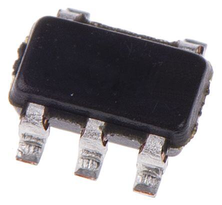
| 描述 | IC REG LDO 1.8V 0.4A SOT23-5低压差稳压器 Cap-Free NMOS 400mA |
| 产品分类 | |
| 品牌 | Texas Instruments |
| 产品手册 | |
| 产品图片 |
|
| rohs | 符合RoHS无铅 / 符合限制有害物质指令(RoHS)规范要求 |
| 产品系列 | 电源管理 IC,低压差稳压器,Texas Instruments TPS73618DBVT- |
| 数据手册 | |
| 产品型号 | TPS73618DBVT |
| PCN设计/规格 | |
| 产品目录页面 | |
| 产品种类 | 低压差稳压器 |
| 供应商器件封装 | SOT-23-5 |
| 其它名称 | 296-15816-2 |
| 制造商产品页 | http://www.ti.com/general/docs/suppproductinfo.tsp?distId=10&orderablePartNumber=TPS73618DBVT |
| 包装 | 带卷 (TR) |
| 商标 | Texas Instruments |
| 回动电压—最大值 | 200 mV at 400 mA |
| 安装类型 | 表面贴装 |
| 安装风格 | SMD/SMT |
| 封装 | Reel |
| 封装/外壳 | SC-74A,SOT-753 |
| 封装/箱体 | SOT-23-5 |
| 工作温度 | -40°C ~ 125°C |
| 工厂包装数量 | 250 |
| 最大功率耗散 | 0.56 W |
| 最大工作温度 | + 125 C |
| 最大输入电压 | 5.5 V |
| 最小工作温度 | - 40 C |
| 最小输入电压 | + 1.7 V |
| 标准包装 | 250 |
| 电压-跌落(典型值) | 0.075V @ 400mA |
| 电压-输入 | 最高 5.5V |
| 电压-输出 | 1.8V |
| 电压调节准确度 | 0.5 % |
| 电流-输出 | 400mA |
| 电流-限制(最小值) | 400mA |
| 稳压器拓扑 | 正,固定式 |
| 稳压器数 | 1 |
| 系列 | TPS73618 |
| 线路调整率 | 0.01 % / V |
| 设计资源 | http://www.digikey.com/product-highlights/cn/zh/texas-instruments-webench-design-center/3176 |
| 负载调节 | 0.002 % / mA |
| 输入偏压电流—最大 | 0.3 mA |
| 输出电压 | 1.8 V |
| 输出电流 | 400 mA |
| 输出端数量 | 1 Output |
| 输出类型 | Fixed |
| 配用 | /product-detail/zh/TPS73633EVM-066/296-19001-ND/863823 |


- 商务部:美国ITC正式对集成电路等产品启动337调查
- 曝三星4nm工艺存在良率问题 高通将骁龙8 Gen1或转产台积电
- 太阳诱电将投资9.5亿元在常州建新厂生产MLCC 预计2023年完工
- 英特尔发布欧洲新工厂建设计划 深化IDM 2.0 战略
- 台积电先进制程称霸业界 有大客户加持明年业绩稳了
- 达到5530亿美元!SIA预计今年全球半导体销售额将创下新高
- 英特尔拟将自动驾驶子公司Mobileye上市 估值或超500亿美元
- 三星加码芯片和SET,合并消费电子和移动部门,撤换高东真等 CEO
- 三星电子宣布重大人事变动 还合并消费电子和移动部门
- 海关总署:前11个月进口集成电路产品价值2.52万亿元 增长14.8%


PDF Datasheet 数据手册内容提取
Product Sample & Technical Tools & Support & Folder Buy Documents Software Community TPS736 SBVS038U–SEPTEMBER2003–REVISEDJANUARY2015 TPS736xx Cap-Free, NMOS, 400-mA Low-Dropout Regulator with Reverse Current Protection 1 Features 3 Description • StablewithNoOutputCapacitororAnyValueor The TPS736xx family of low-dropout (LDO) linear 1 voltage regulators uses a new topology: an NMOS TypeofCapacitor pass element in a voltage-follower configuration. This • InputVoltageRangeof1.7Vto5.5V topology is stable using output capacitors with low • Ultra-LowDropoutVoltage:75mVtyp ESR, and even allows operation without a capacitor. • ExcellentLoadTransientResponse—withor It also provides high reverse blockage (low reverse current)andgroundpincurrentthatisnearlyconstant withoutOptionalOutputCapacitor overallvaluesofoutputcurrent. • NewNMOSTopologyDeliversLowReverse LeakageCurrent The TPS736xx uses an advanced BiCMOS process to yield high precision while delivering very low • LowNoise:30 μV typ(10Hzto100kHz) RMS dropout voltages and low ground pin current. Current • 0.5%InitialAccuracy consumption, when not enabled, is under 1 μA and • 1%OverallAccuracyOverLine,Load,and ideal for portable applications. The extremely low Temperature output noise (30 μVRMS with 0.1-μF CNR) is ideal for powering VCOs. These devices are protected by • LessThan1μAmaxI inShutdownMode Q thermalshutdownandfoldbackcurrentlimit. • ThermalShutdownandSpecifiedMin/Max CurrentLimitProtection DeviceInformation(1) • AvailableinMultipleOutputVoltageVersions PARTNUMBER PACKAGE BODYSIZE(NOM) – FixedOutputsof1.20Vto5.0V SOT-23(5) 2.90mmx1.60mm – AdjustableOutputfrom1.20Vto5.5V TPS736xx SOT-223(6) 6.50mmx3.50mm – CustomOutputsAvailable VSON(8) 3.00mmx3.00mm (1) For all available packages, see the orderable addendum at 2 Applications theendofthedatasheet. • Portable/Battery-PoweredEquipment • Post-RegulationforSwitchingSupplies • Noise-SensitiveCircuitrysuchasVCOs • PointofLoadRegulationforDSPs,FPGAs, ASICs,andMicroprocessors TypicalApplicationCircuitforFixed-VoltageVersions Optional Optional VIN IN OUT VOUT TPS736xx EN GND NR ON OFF Optional 1 An IMPORTANT NOTICE at the end of this data sheet addresses availability, warranty, changes, use in safety-critical applications, intellectualpropertymattersandotherimportantdisclaimers.PRODUCTIONDATA.
TPS736 SBVS038U–SEPTEMBER2003–REVISEDJANUARY2015 www.ti.com Table of Contents 1 Features.................................................................. 1 8 ApplicationandImplementation........................ 15 2 Applications........................................................... 1 8.1 ApplicationInformation............................................15 3 Description............................................................. 1 8.2 TypicalApplications................................................15 4 RevisionHistory..................................................... 2 9 PowerSupplyRecommendations...................... 20 5 PinConfigurationandFunctions......................... 3 10 Layout................................................................... 20 6 Specifications......................................................... 4 10.1 LayoutGuidelines.................................................20 6.1 AbsoluteMaximumRatings......................................4 10.2 LayoutExamples...................................................20 6.2 ESDRatings ............................................................4 10.3 PowerDissipation.................................................21 6.3 RecommendedOperatingConditions.......................4 10.4 ThermalProtection................................................22 6.4 ThermalInformation..................................................5 10.5 PackageMounting................................................22 6.5 ElectricalCharacteristics...........................................6 11 DeviceandDocumentationSupport................. 23 6.6 TypicalCharacteristics..............................................7 11.1 DeviceSupport......................................................23 7 DetailedDescription............................................ 12 11.2 DocumentationSupport........................................23 7.1 Overview.................................................................12 11.3 Trademarks...........................................................23 7.2 FunctionalBlockDiagram.......................................12 11.4 ElectrostaticDischargeCaution............................23 7.3 FeatureDescription.................................................13 11.5 Glossary................................................................23 7.4 DeviceFunctionalModes........................................14 12 Mechanical,Packaging,andOrderable Information........................................................... 23 4 Revision History NOTE:Pagenumbersforpreviousrevisionsmaydifferfrompagenumbersinthecurrentversion. ChangesfromRevisionT(August2010)toRevisionU Page • AddedESDRatingstable,FeatureDescriptionsection,DeviceFunctionalModes,ApplicationandImplementation section,PowerSupplyRecommendationssection,Layoutsection,DeviceandDocumentationSupportsection,and Mechanical,Packaging,andOrderableInformationsection ................................................................................................. 1 • Changed"free-airtemperature"to"junctiontemperature"inAbsoluteMaximumRatingsconditionstatement ...................4 • Changed"free-airtemperature"to"junctiontemperature"inRecommendedOperatingConditionscondition statement ............................................................................................................................................................................... 4 • ChangedThermalInformationtable;updatedthermalresistancevaluesforallpackages .................................................. 5 ChangesfromRevisionS(August,2009)toRevisionT Page • ReplacedDissipationRatingsTablewithThermalInformationTable.................................................................................... 4 ChangesfromRevisionR(May,2008)toRevisionS Page • ChangedFigure10 ................................................................................................................................................................ 7 • Addedparagraphaboutrecommendedstart-upsequencetoInternalCurrentLimitsection.............................................. 14 • Addedparagraphaboutcurrentfoldbackanddevicestart-uptoEnablePinandShutdownsection.................................. 14 2 SubmitDocumentationFeedback Copyright©2003–2015,TexasInstrumentsIncorporated ProductFolderLinks:TPS736
TPS736 www.ti.com SBVS038U–SEPTEMBER2003–REVISEDJANUARY2015 5 Pin Configuration and Functions DBVPackage 5-PinSOT23 DCQPackage (TopView) 6-PinSOT223 (TopView) IN 1 5 OUT 6 GND 2 EN 3 4 NR/FB 1 2 3 4 5 IN GND EN OUT NR/FB DRBPackage 8-PinVSON (TopView) OUT 1 8 IN N/C 2 7 N/C NR/FB 3 6 N/C GND 4 5 EN PinFunctions PIN NO. I/O DESCRIPTION SOT23 SOT22 NAME 3 VSON IN 1 1 8 I Inputsupply GND 2 3,6 4,Pad — Ground Drivingtheenablepin(EN)highturnsontheregulator.Drivingthispinlowputsthe EN 3 5 5 I regulatorintoshutdownmode.RefertotheShutdownsectionformoredetails.ENcan beconnectedtoINifnotused. Fixed-voltageversionsonly.Connectinganexternalcapacitortothisnoisereduction NR 4 4 3 — pinbypassesnoisegeneratedbytheinternalbandgap,reducingoutputnoisetovery lowlevels. Adjustable-voltageversiononly.Thispinistheinputtothecontrollooperroramplifier, FB 4 4 3 I andsetstheoutputvoltageofthedevice. OUT 5 2 1 O Outputoftheregulator.Therearenooutputcapacitorrequirementsforstability. Copyright©2003–2015,TexasInstrumentsIncorporated SubmitDocumentationFeedback 3 ProductFolderLinks:TPS736
TPS736 SBVS038U–SEPTEMBER2003–REVISEDJANUARY2015 www.ti.com 6 Specifications 6.1 Absolute Maximum Ratings overoperatingjunctiontemperaturerange(unlessotherwisenoted) (1) MIN MAX UNIT V –0.3 +6.0 V IN V –0.3 +6.0 V EN Voltage V –0.3 +5.5 V OUT V ,V –0.3 +6.0 V NR FB Peakoutputcurrent I Internallylimited OUT Outputshort-circuitduration Indefinite Continuoustotalpower P SeeThermalInformation dissipation DISS T Junctiontemperaturerange –55 150 °C J T Storagetemperaturerange –65 150 °C stg (1) StressesbeyondthoselistedunderAbsoluteMaximumRatingsmaycausepermanentdamagetothedevice.Thesearestressratings only,whichdonotimplyfunctionaloperationofthedeviceattheseoranyotherconditionsbeyondthoseindicatedunderRecommended OperatingConditions.Exposuretoabsolute-maximum-ratedconditionsforextendedperiodsmayaffectdevicereliability.Electrical CharacteristicsExposuretoabsolutemaximumratedconditionsforextendedperiodsmayaffectdevicereliability 6.2 ESD Ratings VALUE UNIT Humanbodymodel(HBM),perANSI/ESDA/JEDECJS-001,all pins(1) ±2000 V Electrostaticdischarge V (ESD) Chargeddevicemodel(CDM),perJEDECspecification JESD22-C101,allpins(2) ±500 (1) JEDECdocumentJEP155statesthat500-VHBMallowssafemanufacturingwithastandardESDcontrolprocess. (2) JEDECdocumentJEP157statesthat250-VCDMallowssafemanufacturingwithastandardESDcontrolprocess. 6.3 Recommended Operating Conditions overoperatingjunctiontemperaturerange(unlessotherwisenoted) MIN NOM MAX UNIT V Inputsupplyvoltagerange 1.7 5.5 V IN I Outputcurrent 0 500 mA OUT T Operatingjunctiontemperature –40 125 °C J 4 SubmitDocumentationFeedback Copyright©2003–2015,TexasInstrumentsIncorporated ProductFolderLinks:TPS736
TPS736 www.ti.com SBVS038U–SEPTEMBER2003–REVISEDJANUARY2015 6.4 Thermal Information TPS736(3) THERMALMETRIC(1)(2) DRB/SON DCQ/SOT223 DBV/SOT23 UNIT 8PINS 6PINS 5PINS R Junction-to-ambientthermalresistance(4) 52.8 118.7 221.9 θJA R Junction-to-case(top)thermalresistance(5) 60.4 64.9 74.9 θJC(top) R Junction-to-boardthermalresistance(6) 28.4 65.0 51.9 θJB °C/W ψ Junction-to-topcharacterizationparameter(7) 2.1 14.0 2.8 JT ψ Junction-to-boardcharacterizationparameter(8) 28.6 63.8 51.1 JB R Junction-to-case(bottom)thermalresistance(9) 12.0 N/A N/A θJC(bot) (1) Formoreinformationabouttraditionalandnewthermalmetrics,seetheICPackageThermalMetricsapplicationreport,SPRA953. (2) ForthermalestimatesofthisdevicebasedonPCBcopperarea,seetheTIPCBThermalCalculator. (3) ThermaldatafortheDRB,DCQ,andDRVpackagesarederivedbythermalsimulationsbasedonJEDEC-standardmethodologyas specifiedintheJESD51series.Thefollowingassumptionsareusedinthesimulations: (a) i. DRB: The exposed pad is connected to the PCB ground layer through a 2x2 thermal via array. . ii. DCQ: The exposed pad is connected to the PCB ground layer through a 3x2 thermal via array. .iii.DBV:ThereisnoexposedpadwiththeDBVpackage. (b) i.DRB:Thetopandbottomcopperlayersareassumedtohavea20%thermalconductivityofcopperrepresentinga20%copper coverage. . ii. DCQ: Each of top and bottom copper layers has a dedicated pattern for 20% copper coverage. .iii.DBV:Thetopandbottomcopperlayersareassumedtohavea20%thermalconductivityofcopperrepresentinga20%copper coverage. (c)ThesedataweregeneratedwithonlyasingledeviceatthecenterofaJEDEChigh-K(2s2p)boardwith3in×3incopperarea.To understandtheeffectsofthecopperareaonthermalperformance,seethePowerDissipationsectionofthisdatasheet. (4) Thejunction-to-ambientthermalresistanceundernaturalconvectionisobtainedinasimulationonaJEDEC-standard,high-Kboard,as specifiedinJESD51-7,inanenvironmentdescribedinJESD51-2a. (5) Thejunction-to-case(top)thermalresistanceisobtainedbysimulatingacoldplatetestonthetopofthepackage.NospecificJEDEC- standardtestexists,butaclosedescriptioncanbefoundintheANSISEMIstandardG30-88. (6) Thejunction-to-boardthermalresistanceisobtainedbysimulatinginanenvironmentwitharingcoldplatefixturetocontrolthePCB temperature,asdescribedinJESD51-8. (7) Thejunction-to-topcharacterizationparameter,ψ ,estimatesthejunctiontemperatureofadeviceinarealsystemandisextracted JT fromthesimulationdatatoobtainθ usingaproceduredescribedinJESD51-2a(sections6and7). JA (8) Thejunction-to-boardcharacterizationparameter,ψ ,estimatesthejunctiontemperatureofadeviceinarealsystemandisextracted JB fromthesimulationdatatoobtainθ usingaproceduredescribedinJESD51-2a(sections6and7). JA (9) Thejunction-to-case(bottom)thermalresistanceisobtainedbysimulatingacoldplatetestontheexposed(power)pad.Nospecific JEDECstandardtestexists,butaclosedescriptioncanbefoundintheANSISEMIstandardG30-88. Copyright©2003–2015,TexasInstrumentsIncorporated SubmitDocumentationFeedback 5 ProductFolderLinks:TPS736
TPS736 SBVS038U–SEPTEMBER2003–REVISEDJANUARY2015 www.ti.com 6.5 Electrical Characteristics Overoperatingtemperaturerange(T =–40°Cto125°C),V =V +0.5V(1),I =10mA,V =1.7V,and J IN OUT(nom) OUT EN C =0.1μF,unlessotherwisenoted.TypicalvaluesareatT =25°C. OUT J PARAMETER TESTCONDITIONS MIN TYP MAX UNIT V Inputvoltagerange(1)(2) 1.7 5.5 V IN V Internalreference(TPS73601) T =25°C 1.198 1.20 1.210 V FB J Outputvoltagerange (TPS73601)(3) VFB 5.5–VDO V V Nominal T =25°C –0.5 +0.5 OUT J Accuracy(1)(4) overV ,I , V +0.5V≤V ≤5.5V; IN OUT OUT IN –1.0% ±0.5% +1.0% andT 10mA≤I ≤400mA OUT ΔV Lineregulation(1) V +0.5V≤V ≤5.5V 0.01 %/V OUT(ΔVIN) O(nom) IN 1mA≤I ≤400mA 0.002 OUT ΔV Loadregulation %/mA OUT(ΔIOUT) 10mA≤I ≤400mA 0.0005 OUT Dropoutvoltage(5) V I =400mA 75 200 mV DO (V =V –0.1V) OUT IN OUT(nom) Z Outputimpedanceindropout 1.7V≤V ≤V +V 0.25 Ω O(do) IN OUT DO V =0.9×V 400 650 800 mA OUT OUT(nom) I Outputcurrentlimit CL 3.6V≤V ≤4.2V,0°C≤T ≤70°C 500 800 mA IN J I Short-circuitcurrent V =0V 450 mA SC OUT I Reverseleakagecurrent(6)(–I ) V ≤0.5V,0V≤V ≤V 0.1 10 μA REV IN EN IN OUT I =10mA(I ) 400 550 OUT Q I GNDpincurrent μA GND I =400mA 800 1000 OUT V ≤0.5V,V ≤V ≤5.5, I Shutdowncurrent(I ) EN OUT IN 0.02 1 μA SHDN GND –40°C≤T ≤100°C J I FBpincurrent(TPS73601) 0.1 0.3 μA FB Power-supplyrejectionratio f=100Hz,IOUT=400mA 58 PSRR dB (ripplerejection) f=10kHz,I =400mA 37 OUT Outputnoisevoltage COUT=10μF,NoCNR 27×VOUT V μV n BW=10Hz–100KHz C =10μF,C =0.01μF 8.5×V RMS OUT NR OUT V =3V,R =30ΩC =1μF, t Startuptime OUT L OUT 600 μs STR C =0.01μF NR V ENpinhigh(enabled) 1.7 V V EN(high) IN V ENpinlow(shutdown) 0 0.5 V EN(low) I ENpincurrent(enabled) V =5.5V 0.02 0.1 μA EN(high) EN Shutdown,temperatureincreasing 160 T Thermalshutdowntemperature °C SD Reset,temperaturedecreasing 140 T Operatingjunctiontemperature –40 125 °C J (1) MinimumV =V +V or1.7V,whicheverisgreater. IN OUT DO (2) ForV <1.6V,whenV ≤1.6V,theoutputlockstoV andmayresultinadamagingover-voltagelevelontheoutput.Toavoid OUT(nom) IN IN thissituation,disablethedevicebeforepoweringdowntheV . IN (3) TPS73601istestedatV =2.5V. OUT (4) Toleranceofexternalresistorsnotincludedinthisspecification. (5) V isnotmeasuredforfixedoutputversionswithV <1.8V. DO OUT(nom) (6) Fixed-voltageversionsonly;refertoApplicationInformationsectionformoreinformation. 6 SubmitDocumentationFeedback Copyright©2003–2015,TexasInstrumentsIncorporated ProductFolderLinks:TPS736
TPS736 www.ti.com SBVS038U–SEPTEMBER2003–REVISEDJANUARY2015 6.6 Typical Characteristics Forallvoltageversions,atT =25°C,V =V +0.5V,I =10mA,V =1.7V,andC =0.1μF,unlessotherwise J IN OUT(nom) OUT EN OUT noted. 0.5 0.20 0.4 ReferredtoIOUT=10mA 0.15 ReferredtoVIN=VOUT+0.5VatIOUT=10mA 0.3 - 40(cid:1)C V(%)OUT 00..21 ++12255(cid:1)(cid:1)CC V(%)OUT 00..1005 +125(cid:1)C +25(cid:1)C n 0 n 0 ngei - 0.1 ngei - 0.05 ha - 0.2 ha - 40(cid:1)C C C - 0.10 - 0.3 - 0.4 - 0.15 - 0.5 - 0.20 0 50 100 150 200 250 300 350 400 0 0.5 1.0 1.5 2.0 2.5 3.0 3.5 4.0 4.5 IOUT(mA) VIN- VOUT(V) Figure1.LoadRegulation Figure2.LineRegulation 100 100 TPS73625DBV TPS73625DBV +125(cid:1)C IOUT=400mA 80 80 V) 60 V) 60 m +25(cid:1)C m ( ( O O VD 40 VD 40 - 40(cid:1)C 20 20 0 0 0 50 100 150 200 250 300 350 400 - 50 - 25 0 25 50 75 100 125 IOUT(mA) Temperature((cid:1)C) Figure3.DropoutVoltagevsOutputCurrent Figure4.DropoutVoltagevsTemperature 30 18 IOUT=10mA 16 IOUT=10mA 25 AllVoltageVersions 14 %) %) ( 20 ( 12 s s Unit Unit 10 15 of of 8 nt nt e e erc 10 erc 6 P P 4 5 2 0 0 098765432101234567890 000000000000000000000 1.0.0.0.0.0.0.0.0.0. 0.0.0.0.0.0.0.0.0.1. 10987654321 12345678910 --------V--Error(%) -----W-o-rst-Ca-se-dV /dT(ppm/(cid:1)C) OUT OUT Figure5.OutputVoltageAccuracyHistogram Figure6.OutputVoltageDriftHistogram Copyright©2003–2015,TexasInstrumentsIncorporated SubmitDocumentationFeedback 7 ProductFolderLinks:TPS736
TPS736 SBVS038U–SEPTEMBER2003–REVISEDJANUARY2015 www.ti.com Typical Characteristics (continued) Forallvoltageversions,atT =25°C,V =V +0.5V,I =10mA,V =1.7V,andC =0.1μF,unlessotherwise J IN OUT(nom) OUT EN OUT noted. 1000 1000 I =400mA 900 900 OUT 800 800 700 700 A) 600 A) 600 m( 500 m( 500 D D N N G400 G400 I I 300 300 200 VIN=5.5V 200 VIN=5.5V 100 VVIN==42VV 100 VVIN==32VV IN IN 0 0 0 100 200 300 400 - 50 - 25 0 25 50 75 100 125 IOUT(mA) Temperature((cid:1)C) Figure7.GroundPinCurrentvsOutputCurrent Figure8.GroundPinCurrentvsTemperature 1 800 V =0.5V TPS73633 VENA=BVLE +0.5V 700 IN O I CL A) 600 m m(A)ND0.1 Current ( 540000 ISC IG ut 300 p ut O 200 100 0.01 0 - 50 - 25 0 25 50 75 100 125 -0.5 0 0.5 1.0 1.5 2.0 2.5 3.0 3.5 Temperature((cid:1)C) Output Voltage (V) Figure9.GroundPinCurrentInShutdownvsTemperature Figure10.CurrentLimitvsVOUT(Foldback) 800 800 750 750 700 700 A) A) m 650 m 650 ( ( mit mit Li 600 Li 600 nt nt e 550 e 550 urr urr C C 500 500 450 450 400 400 1.5 2.0 2.5 3.0 3.5 4.0 4.5 5.0 5.5 - 50 - 25 0 25 50 75 100 125 V (V) Temperature((cid:1)C) IN Figure11.CurrentLimitvsV Figure12.CurrentLimitvsTemperature IN 8 SubmitDocumentationFeedback Copyright©2003–2015,TexasInstrumentsIncorporated ProductFolderLinks:TPS736
TPS736 www.ti.com SBVS038U–SEPTEMBER2003–REVISEDJANUARY2015 Typical Characteristics (continued) Forallvoltageversions,atT =25°C,V =V +0.5V,I =10mA,V =1.7V,andC =0.1μF,unlessotherwise J IN OUT(nom) OUT EN OUT noted. 90 40 I =100mA I =1mA 80 COOUUTT=Any COOUUTT=1m F 35 70 B) IOUT=1mA 30 Rejection(d 654000 ICOOUUTT==1AmnAy COUT=10m F IOC=O10=01mm AF SRR (dB) 2250 e P 15 pl 30 Rip 2100 IOUT=Any ICOOUUTT==11000mmFA 105 FCVrOOeUUqTTu==e n21c.05ym V=F 10kHz VIN=VOUT+1V COUT=0m F IOUT= 100mA 0 0 10 100 1k 10k 100k 1M 10M 0 0.2 0.4 0.6 0.8 1.0 1.2 1.4 1.6 1.8 2.0 Frequency(Hz) VIN-VOUT(V) Figure13. PSRR(RippleRejection)vsFrequency Figure14. PSRR(RippleRejection)vsVIN–VOUT 1 1 C =1m F OUT √Hz) COUT=0m F √Hz) COUT=1m F V/ 0.1 V/ 0.1 C =10m F m( OUT m( N N e e C =0m F OUT C =10m F OUT IOUT=150mA IOUT=150mA 0.01 0.01 10 100 1k 10k 100k 10 100 1k 10k 100k Frequency(Hz) Frequency(Hz) Figure15.NoiseSpectralDensitycNR=0μF Figure16.NoiseSpectralDensitycNR=0.01μF 60 140 V =5.0V OUT 50 120 V =5.0V OUT 100 40 MS) MS) 80 VOUT=3.3V (RN 30 VOUT=3.3V (RN 60 V V 20 40 V =1.5V V =1.5V OUT OUT 10 CNR=0.01m F 20 COUT=0m F 10Hz<Frequency<100kHz 10Hz<Frequency<100kHz 0 0 0.1 1 10 1p 10p 100p 1n 10n C (m F) C (F) OUT NR Figure17.RMSNoiseVoltagevsCOUT Figure18.RMSNoiseVoltagevsCNR Copyright©2003–2015,TexasInstrumentsIncorporated SubmitDocumentationFeedback 9 ProductFolderLinks:TPS736
TPS736 SBVS038U–SEPTEMBER2003–REVISEDJANUARY2015 www.ti.com Typical Characteristics (continued) Forallvoltageversions,atT =25°C,V =V +0.5V,I =10mA,V =1.7V,andC =0.1μF,unlessotherwise J IN OUT(nom) OUT EN OUT noted. VIN=3.8V COUT=0m F IOUT=400mA 100mV/tick V OUT C =0m F OUT 50mV/div V C =1m F OUT OUT 50mV/tick V OUT 20mV/tick COUT=10m F VOUT 50mV/div COUT=100m F VOUT dV 5.5V IN=0.5V/m s 400mA dt 50mA/tick IOUT 4.5V 10mA 1V/div VIN 10m s/div 10m s/div Figure19.TPS73633LoadTransientResponse Figure20.TPS73633LineTransientResponse RCLOU=T1=kW0m F VOUT RCLOU=T2=0W10m F 1V/div RCLOU=T2=0W1m F 1V/div RCLOU=T2=0W1m F R =1kW RCL=2=0W10m F CLOUT=0m F OUT V OUT 2V 2V V EN 1V/div 1V/div 0V 0V V EN 100m s/div 100m s/div Figure21.TPS73633Turn-OnResponse Figure22.TPS73633Turn-OffResponse 6 10 5 V IN 4 V OUT 1 3 A) n s ( Volt 2 BLE A 1 EN I 0.1 0 - 1 - 2 0.01 50ms/div - 50 - 25 0 25 50 75 100 125 Temperature((cid:1)C) Figure23.TPS73633PowerUp/PowerDown Figure24.I vsTemperature ENABLE 10 SubmitDocumentationFeedback Copyright©2003–2015,TexasInstrumentsIncorporated ProductFolderLinks:TPS736
TPS736 www.ti.com SBVS038U–SEPTEMBER2003–REVISEDJANUARY2015 Typical Characteristics (continued) Forallvoltageversions,atT =25°C,V =V +0.5V,I =10mA,V =1.7V,andC =0.1μF,unlessotherwise J IN OUT(nom) OUT EN OUT noted. 60 160 55 140 50 120 45 100 V(rms)N 4305 I(nA)FB 8600 V =2.5V 30 COUT=0m F 40 OUT 25 R1=39.2kW 20 10Hz<Frequency<100kHz 20 0 10p 100p 1n 10n - 50 - 25 0 25 50 75 100 125 C (F) Temperature((cid:1)C) FB Figure25.TPS73601RMSNoiseVoltagevsCFB Figure26.TPS73601IFBvsTemperature 200mV/div CRF1B==3190.2nkFW COUT=0m F VOUT 100mV/div COUT=0m F VCOFUBT==120.5nVF VOUT C =10m F OUT 100mV/div V OUT C =10m F 200mV/div OUT V OUT 4.5V 400mA 3.5V V IN 10mA I OUT 25m s/div 5m s/div Figure27.TPS73601LoadTransient,AdjustableVersion Figure28.TPS73601LineTransient,AdjustableVersion Copyright©2003–2015,TexasInstrumentsIncorporated SubmitDocumentationFeedback 11 ProductFolderLinks:TPS736
TPS736 SBVS038U–SEPTEMBER2003–REVISEDJANUARY2015 www.ti.com 7 Detailed Description 7.1 Overview The TPS736xx family of low-dropout linear regulators operates down to an input voltage of 1.7 V and supports output voltages down to 1.2 V while sourcing up to 500 mA of load current. This linear regulator utilizes an NMOS pass element with an integrated 4-MHz charge pump to provide a dropout voltage of less than 200 mV at fullloadcurrent.Thisuniquearchitecturealsopermitsstableregulationoverawiderangeofoutputcapacitors.In fact, the TPS736xx family of devices does not require any output capacitor for stability. The increased insensitivity to the output capacitor value and type makes this family of linear regulators an ideal choice when poweringaloadwheretheeffectivecapacitanceisunknown. The TPS736xx family of devices also features a noise reduction (NR) pin that allows for additional reduction of the output noise. With a noise reduction capacitor of 0.01 µF connected from the NR pin to GND, the TPS73615 outputnoisecanbeaslowas12.75µV .ThelownoiseoutputfeaturedbytheTPS736xxfamilymakesitwell- RMS suitedforpoweringVCOsoranyothernoisesensitiveload. 7.2 Functional Block Diagram IN 4MHz ChargePump EN Thermal Protection Ref Servo 27kW Bandgap Error Amp Current Limit OUT 8kW GND R 1 R1+R2=80kW R2 NR Figure29. Fixed-VoltageVersion 12 SubmitDocumentationFeedback Copyright©2003–2015,TexasInstrumentsIncorporated ProductFolderLinks:TPS736
TPS736 www.ti.com SBVS038U–SEPTEMBER2003–REVISEDJANUARY2015 Functional Block Diagram (continued) IN Standard 1% Resistor Values for Common Output Voltages 4MHz ChargePump VO R1 R2 1.2V Short Open EN Thermal 1.5V 23.2kW 95.3kW Protection Ref 1.8V 28.0kW 56.2kW Servo 2.5V 39.2kW 36.5kW 27kW 2.8V 44.2kW 33.2kW Bandgap Error 3.0V 46.4kW 30.9kW Amp 3.3V 52.3kW 30.1kW OUT Current Limit NOTE: VOUT= (R1+ R2)/R2×1.204; GND 8kW 80kW R1||R2@19kWfor best R1 accuracy. FB R 2 Figure30. Adjustable-VoltageVersion 7.3 Feature Description 7.3.1 OutputNoise A precision band-gap reference is used to generate the internal reference voltage, V . This reference is the REF dominant noise source within the TPS736xx and it generates approximately 32 μV (10 Hz to 100 kHz) at the RMS reference output (NR). The regulator control loop gains up the reference noise with the same gain as the referencevoltage,sothatthenoisevoltageoftheregulatorisapproximatelygivenby: (R (cid:2)R ) V V (cid:3)32(cid:1)V (cid:1) 1 2 (cid:3)32(cid:1)V (cid:1) OUT N RMS R2 RMS VREF (1) SincethevalueofV is1.2V,thisrelationshipreducesto: REF (cid:3)(cid:1)V (cid:4) VN((cid:1)VRMS)(cid:2)27 VRMS (cid:1)VOUT(V) (2) forthecaseofnoC . NR An internal 27-kΩ resistor in series with the noise reduction pin (NR) forms a low-pass filter for the voltage reference when an external noise reduction capacitor, C , is connected from NR to ground. For C = 10 nF, NR NR the total noise in the 10-Hz to 100-kHz bandwidth is reduced by a factor of ~3.2, giving the approximate relationship: (cid:3)(cid:1)V (cid:4) VN((cid:1)VRMS)(cid:2)8.5 VRMS (cid:1)VOUT(V) (3) forC =10nF. NR ThisnoisereductioneffectisshownasRMSNoiseVoltagevsC intheTypicalCharacteristicssection. NR Copyright©2003–2015,TexasInstrumentsIncorporated SubmitDocumentationFeedback 13 ProductFolderLinks:TPS736
TPS736 SBVS038U–SEPTEMBER2003–REVISEDJANUARY2015 www.ti.com Feature Description (continued) The TPS73601 adjustable version does not have the NR pin available. However, connecting a feedback capacitor, C , from the output to the feedback pin (FB) reduces output noise and improves load transient FB performance. The TPS736xx uses an internal charge pump to develop an internal supply voltage sufficient to drive the gate of the NMOS pass element above V . The charge pump generates ~250 μV of switching noise at ~4 MHz; OUT however, charge-pump noise contribution is negligible at the output of the regulator for most values of I and OUT C . OUT 7.3.2 InternalCurrentLimit The TPS736xx internal current limit helps protect the regulator during fault conditions. Foldback current limit helps to protect the regulator from damage during output short-circuit conditions by reducing current limit when V dropsbelow0.5V.SeeFigure10intheTypicalCharacteristicssection. OUT Note from Figure 10 that approximately –0.2 V of V results in a current limit of 0 mA. Therefore, if OUT is OUT forced below –0.2 V before EN goes high, the device may not start up. In applications that work with both a positiveandnegativevoltagesupply,the TPS736xxshouldbeenabledfirst. 7.3.3 EnablePinandShutdown The enable pin (EN) is active high and is compatible with standard TTL-CMOS levels. V below 0.5 V (max) EN turns the regulator off and drops the GND pin current to approximately 10 nA. When EN is used to shutdown the regulator, all charge is removed from the pass transistor gate, and the output ramps back up to a regulated V OUT (seeFigure19). When shutdown capability is not required, EN can be connected to V . However, the pass gate may not be IN discharged using this configuration, and the pass transistor may be left on (enhanced) for a significant time after V hasbeenremoved.Thisscenariocanresultinreversecurrentflow(iftheINpinislowimpedance)andfaster IN ramp times upon power-up. In addition, for V ramp times slower than a few milliseconds, the output may IN overshootuponpower-up. Note that current limit foldback can prevent device start-up under some conditions. See the Internal Current Limit sectionformoreinformation. 7.3.4 ReverseCurrent The NMOS pass element of the TPS736xx provides inherent protection against current flow from the output of the regulator to the input when the gate of the pass device is pulled low. To ensure that all charge is removed from the gate of the pass element, the EN pin must be driven low before the input voltage is removed. If this is notdone,thepasselementmaybeleftonduetostoredchargeonthegate. After the EN pin is driven low, no bias voltage is needed on any pin for reverse current blocking. Note that reverse current is specified as the current flowing out of the IN pin due to voltage applied on the OUT pin. There is additional current flowing into the OUT pin due to the 80-kΩ internal resistor divider to ground (see Figure 29 andFigure30). FortheTPS73601,reversecurrentmayflowwhenV ismorethan1.0VaboveV . FB IN 7.4 Device Functional Modes 7.4.1 NormalOperationwith1.7V ≤ V ≤ 5.5VandV ≥ 1.7V IN EN The TPS736xx family requires an input voltage of at least 1.7 V to function properly and attempt to maintain regulation. Please note that if the device output voltage is greater than 1.5 V when the input voltage is at 1.7 V, the device is operating in dropout and regulation cannot be maintained. Due the NMOS architecture used in the TPS736xxdevices,thedropoutvoltageisnotastrongfunctionoftheinputvoltage. When operating the device near 5.5 V, take care to suppress any transient spikes that may exceed the 6.0-V absolutemaximumvoltagerating.Thedeviceshouldneveroperateatadcvoltagegreaterthan5.5V. 14 SubmitDocumentationFeedback Copyright©2003–2015,TexasInstrumentsIncorporated ProductFolderLinks:TPS736
TPS736 www.ti.com SBVS038U–SEPTEMBER2003–REVISEDJANUARY2015 8 Application and Implementation NOTE Information in the following applications sections is not part of the TI component specification, and TI does not warrant its accuracy or completeness. TI’s customers are responsible for determining suitability of components for their purposes. Customers should validateandtesttheirdesignimplementationtoconfirmsystemfunctionality. 8.1 Application Information The TPS736xx belongs to a family of new generation LDO regulators that use an NMOS pass transistor to achieve ultra-low-dropout performance, reverse current blockage, and freedom from output capacitor constraints. These features, combined with low noise and an enable input, make the TPS736xx ideal for portable applications. This regulator family offers a wide selection of fixed output voltage versions and an adjustable outputversion.Allversionshavethermalandover-currentprotection,includingfoldbackcurrentlimit. 8.2 Typical Applications Figure 31 shows the basic circuit connections for the fixed voltage models. Figure 32 gives the connections for theadjustableoutputversion(TPS73601). Optional input capacitor. Optional output capacitor. May improve source May improve load transient, impedance, noise, or PSRR. noise, or PSRR. VIN IN OUT VOUT TPS736xx EN GND NR ON OFF Optional bypass capacitor to reduce output noise. Figure31. TypicalApplicationCircuitforFixed-VoltageVersions Optional input capacitor. Optional output capacitor. May improve source May improve load transient, impedance, noise, or PSRR. noise, or PSRR. VIN IN OUT VOUT TPS73601 R C 1 FB EN GND FB ON R OFF 2 (R +R) Optional capacitor VOUT= 1R 2 x 1.204 reduces output noise 2 and improves transient response. Figure32. TypicalApplicationCircuitforAdjustable-VoltageVersion Copyright©2003–2015,TexasInstrumentsIncorporated SubmitDocumentationFeedback 15 ProductFolderLinks:TPS736
TPS736 SBVS038U–SEPTEMBER2003–REVISEDJANUARY2015 www.ti.com Typical Applications (continued) 8.2.1 DesignRequirements Forthisdesignexample,usetheparameterslistedinTable1belowastheinputparameters. Table1.DesignParameters(Fixed-VoltageVersion) PARAMETER DESIGNREQUIREMENT Inputvoltage 5V,±3% Outputvoltage 3.3V,±1% Outputcurrent 500mA(maximum),20mA(minimum) RMSnoise,10Hzto100kHz <30μV RMS Ambienttemperature 55°C(Maximum) Table2.DesignParameters(Adjustable-VoltageVersion) PARAMETER DESIGNREQUIREMENT Inputvoltage 5V,±3%,providedbythedc/dcconverterswitchingat1MHz Outputvoltage 2.5V,±1% Outputcurrent 0.4A(maximum),10mA(minimum) RMSnoise,10Hzto100kHz <35μV RMS Ambienttemperature 55°C(Maximum) 8.2.2 DetailedDesignProcedure The first step when designing with a linear regulator is to examine the maximum load current along with the input and output voltage requirements to determine if the device thermal and dropout voltage requirements can be met.At0.5A,thedropoutvoltageoftheTPS73633isamaximumof200mVovertemperature;thus,thedropout headroomissufficientforoperationoverbothinputandoutputvoltageaccuracy. The maximum power dissipated in the linear regulator is the maximum voltage dropped across the pass element from the input to the output times the maximum load current. In this example, the maximum voltage drop across in the pass element is 5 V + 3% (5.15 V) minus 3.3 V – 1% (3.267 V) or 1.883 V. The power dissipated in the pass element is calculated by taking this voltage drop multiplied by the maximum load current. For this example, the maximum power dissipated in the linear regulator is 942 mW. Once the power dissipated in the linear regulator is known, the corresponding junction temperature rise can be calculated. To calculate the junction temperature rise above ambient, the power dissipated must be multiplied by the junction-to-ambient thermal resistance. For thermal resistance information please refer to Thermal Protection. For this example, using the DRB package, the maximum junction temperature rise is calculated to be 45°C. The maximum junction temperature rise is calculated by adding junction temperature rise to the maximum ambient temperature. In this example, the maximum junction temperature is 100°C. Keep in mind the maximum junction temperate must be below 125°C for reliable operation. Addition ground planes, added thermal vias, and air flow all help to lower the maximum junction temperature. Using the DCQ or DBV packages are not recommended for this application due totheexcessivejunctiontemperaturerisethatwouldbeincurred. To get the noise level below 30 µV , a noise reduction capacitance (C ) of 10 nF is selected along with an RMS NR output capacitance of 10 μF. Referencing the Output Noise section, the RMS noise can be calculated to be 28µV . RMS Use of an input capacitor is optional. However, in systems where the input supply is located several inches away from the LDO, a small 0.1-µF input capacitor is recommended to negate the adverse effects that input supply inductancehasonstabilityandacperformance. In the same way as with designing with a fixed output voltage, the first step is to examine the maximum load current along with the input and output voltage requirements to determine if the device thermal and dropout voltagerequirementsaremet.At0.4A,themaximumdropoutvoltagecanbeapproximatedbyassumingalinear characteristic of the dropout voltage with load current. The maximum dropout voltage can be estimated to be 200mVtimestheratiooftheloadcurrenttospecifieddropoutvoltageloadcurrent.Forthisexample,thedropout can be estimated to be 200 mV × 400 mA/500 mA or 160 mV. Since the input voltage is 5 V and the output voltageis2.5V,thereismorethansufficientvoltageheadroomtoavoiddropoutandmaintaingoodPSRR. 16 SubmitDocumentationFeedback Copyright©2003–2015,TexasInstrumentsIncorporated ProductFolderLinks:TPS736
TPS736 www.ti.com SBVS038U–SEPTEMBER2003–REVISEDJANUARY2015 The maximum power dissipated in the linear regulator is the maximum voltage dropped across the pass element from the input to the output times the maximum load current. In this example, the maximum voltage drop across in the pass element is 5 V + 3% (5.15 V) minus 2.5 V – 1% (2.475 V) or 2.675 V. The power dissipated in the pass element is calculated by taking this voltage drop multiplied by the maximum load current. For this example, themaximumpowerdissipatedinthelinearregulatoris1.07W.Oncethepowerdissipatedinthelinearregulator is known, the corresponding junction temperature rise can be calculated. To calculate the junction temperature rise above ambient, the power dissipated must be multiplied by the junction-to-ambient thermal resistance. For thermal resistance information, refer to Thermal Information. For this example, using the DRB package, the maximum junction temperature rise is calculated to be 51°C. The maximum junction temperature rise is calculated by adding junction temperature rise to the maximum ambient temperature. In this example, the maximum junction temperature is 106°C. Keep in mind the maximum junction temperate must be below 125°C for reliable operation. Addition ground planes, added thermal vias, and air flow all help to lower the maximum junction temperature. Using the DCQ or DBV packages are not recommended for this application due to the excessivejunctiontemperaturerisethatwouldbeincurred. R and R can be calculated for any output voltage using the formula shown in Figure 32. Sample resistor values 1 2 forcommonoutputvoltagesareshowninFigure30. For best accuracy, make the parallel combination of R and R approximately equal to 19 kΩ. This 19 kΩ, in 1 2 addition to the internal 8-kΩ resistor, presents the same impedance to the error amp as the 27-kΩ bandgap referenceoutput.Thisimpedancehelpscompensateforleakagesintotheerrorampterminals. Using the values shown in Figure 40xx for a 2.5-V output results in a values of 39.2 kΩ for R and 36.5 kΩ for 1 R . 2 To get the noise level below 35 µV , a noise reduction capacitance (C ) of 10 nF is selected. Figure 25 RMS FF shouldbeusedasareferencewhenselectingoptimalvalueforC . FF A 10-µF, low equivalent series resistance (ESR) ceramic X5R capacitor was used on the output of this design to minimize the output voltage droop during a low transient. Use of an input capacitor is optional. However, in systems where the input supply is located several inches away from the LDO, a small 0.1-µF input capacitor is recommended to negate the adverse effects that input supply inductance has on stability and ac performance. Refer to Input and Output Capacitor Requirements for additional information about input and output capacitor selection. 8.2.2.1 InputandOutputCapacitorRequirements Although an input capacitor is not required for stability, it is good analog design practice to connect a 0.1-μF to 1-μF, low ESR capacitor across the input supply near the regulator. This capacitor counteracts reactive input sources and improves transient response, noise rejection, and ripple rejection. A higher-value capacitor may be necessary if large, fast rise-time load transients are anticipated or the device is located several inches from the powersource. The TPS736xx does not require an output capacitor for stability and has maximum phase margin with no capacitor. It is designed to be stable for all available types and values of capacitors. In applications where multiple low ESR capacitors are in parallel, ringing may occur when the product of C and total ESR drops OUT below 50 nΩF. Total ESR includes all parasitic resistances, including capacitor ESR and board, socket, and solder joint resistance. In most applications, the sum of capacitor ESR and trace resistance meets this requirement. Copyright©2003–2015,TexasInstrumentsIncorporated SubmitDocumentationFeedback 17 ProductFolderLinks:TPS736
TPS736 SBVS038U–SEPTEMBER2003–REVISEDJANUARY2015 www.ti.com 8.2.2.2 DropoutVoltage The TPS736xx uses an NMOS pass transistor to achieve extremely low dropout. When (V – V ) is less than IN OUT the dropout voltage (V ), the NMOS pass device is in its linear region of operation and the input-to-output DO resistanceistheR oftheNMOSpasselement. DS(on) For large step changes in load current, the TPS736xx requires a larger voltage drop from V to V to avoid IN OUT degraded transient response. The boundary of this transient dropout region is approximately twice the dc dropout.ValuesofV –V abovethislineensurenormaltransientresponse. IN OUT Operating in the transient dropout region can cause an increase in recovery time. The time required to recover from a load transient is a function of the magnitude of the change in load current rate, the rate of change in load current, and the available headroom (V to V voltage drop). Under worst-case conditions [full-scale IN OUT instantaneous load change with (V – V ) close to dc dropout levels], the TPS736xx can take a couple of IN OUT hundredmicrosecondstoreturntothespecifiedregulationaccuracy. 8.2.2.3 TransientResponse The low open-loop output impedance provided by the NMOS pass element in a voltage follower configuration allows operation without an output capacitor for many applications. As with any regulator, the addition of a capacitor (nominal value 1 μF) from the OUT pin to ground reduces undershoot magnitude but increase its duration.Intheadjustableversion,theadditionofacapacitor,C ,fromtheOUTpintotheFBpinalsoimproves FB thetransientresponse. The TPS736xx does not have active pull-down when the output is over-voltage. This feature allows applications that connect higher voltage sources, such as alternate power supplies, to the output. This feature also results in an output overshoot of several percent if load current quickly drops to zero when a capacitor is connected to the output. The duration of overshoot can be reduced by adding a load resistor. The overshoot decays at a rate determinedbyoutputcapacitorC andtheinternal/externalloadresistance.Therateofdecayisgivenby: OUT (Fixed Voltage Version) V dV(cid:4)dt(cid:2) OUT C (cid:1)80k(cid:1)(cid:3)R OUT LOAD (4) (Adjustable Voltage Version) V dV(cid:5)dt(cid:3) OUT C (cid:1)80k(cid:1)(cid:4)(R (cid:2)R )(cid:4)R OUT 1 2 LOAD (5) 18 SubmitDocumentationFeedback Copyright©2003–2015,TexasInstrumentsIncorporated ProductFolderLinks:TPS736
TPS736 www.ti.com SBVS038U–SEPTEMBER2003–REVISEDJANUARY2015 8.2.3 ApplicationCurves RCLOU=T1=kW0m F VOUT 100mV/tick VIN=3.8V COUT=0m F VOUT 1V/div RCL=2=0W1m F OUT C =1m F OUT RCL=2=0W10m F 50mV/tick VOUT OUT 2V COUT=10m F V 20mV/tick V EN OUT 1V/div 400mA 0V 50mA/tick IOUT 10mA 100m s/div 10m s/div Figure33.TPS73633Turn-OnResponse Figure34.TPS73633LoadTransientResponse 60 C =10nF FB 55 R1=39.2kW C =0m F 50 200mV/div OUT VOUT 45 s) m V(rN 4305 200mV/div COUT=10m F VOUT V =2.5V 30 COUT=0m F OUT 400mA 25 R1=39.2kW 10Hz<Frequency<100kHz 10mA I 20 OUT 10p 100p 1n 10n 25m s/div C (F) FB Figure35.TPS73601RMSNoiseVoltagevsC Figure36.TPS73601LoadTransient,AdjustableVersion FB Copyright©2003–2015,TexasInstrumentsIncorporated SubmitDocumentationFeedback 19 ProductFolderLinks:TPS736
TPS736 SBVS038U–SEPTEMBER2003–REVISEDJANUARY2015 www.ti.com 9 Power Supply Recommendations This device is designed to operate with an input supply range of 1.7 V to 5.5 V. If the input supply is noisy, additionalinputcapacitorswithlowESRcanhelpimproveoutputnoiseperformance. 10 Layout 10.1 Layout Guidelines To improve ac performance such as PSRR, output noise, and transient response, it is recommended that the board be designed with separate ground planes for V and V , with each ground plane connected only at the IN OUT GND pin of the device. In addition, the ground connection for the bypass capacitor should connect directly to the GNDpinofthedevice. 10.2 Layout Examples GND PLANE COUT VIN TPS736xxDRB VOUT 1 8 N/C 2 7 N/C CIN NR/FB 3 6 N/C 4 5 EN CNR GND PLANE Figure37. FixedOutputVoltageOptionLayout(DRBPackage) 20 SubmitDocumentationFeedback Copyright©2003–2015,TexasInstrumentsIncorporated ProductFolderLinks:TPS736
TPS736 www.ti.com SBVS038U–SEPTEMBER2003–REVISEDJANUARY2015 Layout Examples (continued) GND PLANE COUT VOUT VIN TPS73601DRB 1 8 CFF R1 N/C 2 7 N/C CIN NR/FB 3 6 N/C 4 5 EN R2 GND PLANE Figure38. AdjustableOutputVoltageOptionLayout(DRBPackage) 10.3 Power Dissipation The ability to remove heat from the die is different for each package type, presenting different considerations in the PCB layout. The PCB area around the device that is free of other components moves the heat from the device to the ambient air. Performance data for JEDEC low- and high-K boards are shown in the Thermal Information table. Using heavier copper increases the effectiveness in removing heat from the device. The additionofplatedthrough-holestoheat-dissipatinglayersalsoimprovestheheat-sinkeffectiveness. Powerdissipationdependsoninputvoltageandloadconditions.Powerdissipation(P )isequaltotheproductof D theoutputcurrenttimesthevoltagedropacrosstheoutputpasselement(V toV ): IN OUT space P (cid:3)(V (cid:2)V )(cid:1)I D IN OUT OUT (6) Power dissipation can be minimized by using the lowest possible input voltage necessary to assure the required outputvoltage. Copyright©2003–2015,TexasInstrumentsIncorporated SubmitDocumentationFeedback 21 ProductFolderLinks:TPS736
TPS736 SBVS038U–SEPTEMBER2003–REVISEDJANUARY2015 www.ti.com 10.4 Thermal Protection Thermal protection disables the output when the junction temperature rises to approximately 160°C, allowing the device to cool. When the junction temperature cools to approximately 140°C, the output circuitry is again enabled. Depending on power dissipation, thermal resistance, and ambient temperature, the thermal protection circuit may cycle on and off. This limits the dissipation of the regulator, protecting it from damage due to overheating. Any tendency to activate the thermal protection circuit indicates excessive power dissipation or an inadequate heat sink. For reliable operation, junction temperature should be limited to 125°C maximum. To estimate the margin of safety in a complete design (including heat sink), increase the ambient temperature until the thermal protection is triggered; use worst-case loads and signal conditions. For good reliability, thermal protection should trigger at least 35°C above the maximum expected ambient condition of your application. This produces a worst- casejunctiontemperatureof125°Catthehighestexpectedambienttemperatureandworst-caseload. The internal protection circuitry of the TPS736xx has been designed to protect against overload conditions. It was not intended to replace proper heat sinking. Continuously running the TPS736xx into thermal shutdown degradesdevicereliability. 10.5 Package Mounting Solder pad footprint recommendations for the TPS736xx are presented in Application Note Solder Pad Recommendations for Surface-Mount Devices (SBFA015), available from the Texas Instruments web site at www.ti.com. 22 SubmitDocumentationFeedback Copyright©2003–2015,TexasInstrumentsIncorporated ProductFolderLinks:TPS736
TPS736 www.ti.com SBVS038U–SEPTEMBER2003–REVISEDJANUARY2015 11 Device and Documentation Support 11.1 Device Support 11.1.1 DevelopmentSupport 11.1.1.1 EvaluationModules An evaluation module (EVM) is available to assist in the initial circuit performance evaluation using the TPS736xx. The TPS73601DRBEVM-518 evaluation module (and related user guide) can be requested at the TexasInstrumentswebsitethroughtheproductfoldersorpurchaseddirectlyfromtheTIeStore. 11.1.1.2 SpiceModels Computer simulation of circuit performance using SPICE is often useful when analyzing the performance of analog circuits and systems. A SPICE model for the TPS736 is available through the product folders under SimulationModels. 11.1.2 DeviceNomenclature Table3.DeviceNomenclature(1) PRODUCT V OUT TPS736xxyyyz XXisthenominaloutputvoltage(forexample,25=2.5V;01=Adjustable). YYYisthepackagedesignator. Zisthetapeandreelquantity(R=3000,T=250). (1) ForthemostcurrentpackageandorderinginformationseethePackageOptionAddendumattheendofthisdocument,orseetheTI websiteatwww.ti.com. 11.2 Documentation Support 11.2.1 RelatedDocumentation • Applicationnote.RegulatingV Below1.2VUsinganExternalReference.LiteraturenumberSLVA216. OUT • TPS73x01DRBEVM-518User'sGuide.LiteraturenumberSBVU014. 11.3 Trademarks Alltrademarksarethepropertyoftheirrespectiveowners. 11.4 Electrostatic Discharge Caution Thesedeviceshavelimitedbuilt-inESDprotection.Theleadsshouldbeshortedtogetherorthedeviceplacedinconductivefoam duringstorageorhandlingtopreventelectrostaticdamagetotheMOSgates. 11.5 Glossary SLYZ022—TIGlossary. Thisglossarylistsandexplainsterms,acronyms,anddefinitions. 12 Mechanical, Packaging, and Orderable Information The following pages include mechanical, packaging, and orderable information. This information is the most current data available for the designated devices. This data is subject to change without notice and revision of thisdocument.Forbrowser-basedversionsofthisdatasheet,refertotheleft-handnavigation. Copyright©2003–2015,TexasInstrumentsIncorporated SubmitDocumentationFeedback 23 ProductFolderLinks:TPS736
PACKAGE OPTION ADDENDUM www.ti.com 6-Feb-2020 PACKAGING INFORMATION Orderable Device Status Package Type Package Pins Package Eco Plan Lead/Ball Finish MSL Peak Temp Op Temp (°C) Device Marking Samples (1) Drawing Qty (2) (6) (3) (4/5) TPS73601DBVR ACTIVE SOT-23 DBV 5 3000 Green (RoHS NIPDAU Level-1-260C-UNLIM -40 to 125 PJFQ & no Sb/Br) TPS73601DBVRG4 ACTIVE SOT-23 DBV 5 3000 Green (RoHS NIPDAU Level-1-260C-UNLIM -40 to 125 PJFQ & no Sb/Br) TPS73601DBVT ACTIVE SOT-23 DBV 5 250 Green (RoHS NIPDAU Level-1-260C-UNLIM -40 to 125 PJFQ & no Sb/Br) TPS73601DBVTG4 ACTIVE SOT-23 DBV 5 250 Green (RoHS NIPDAU Level-1-260C-UNLIM -40 to 125 PJFQ & no Sb/Br) TPS73601DCQ ACTIVE SOT-223 DCQ 6 78 Green (RoHS SN Level-2-260C-1 YEAR -40 to 125 PS73601 & no Sb/Br) TPS73601DCQG4 ACTIVE SOT-223 DCQ 6 78 Green (RoHS NIPDAU Level-2-260C-1 YEAR -40 to 125 PS73601 & no Sb/Br) TPS73601DCQR ACTIVE SOT-223 DCQ 6 2500 Green (RoHS SN Level-2-260C-1 YEAR -40 to 125 PS73601 & no Sb/Br) TPS73601DCQRG4 ACTIVE SOT-223 DCQ 6 2500 Green (RoHS NIPDAU Level-2-260C-1 YEAR -40 to 125 PS73601 & no Sb/Br) TPS73601DRBR ACTIVE SON DRB 8 3000 Green (RoHS NIPDAU Level-2-260C-1 YEAR -40 to 125 PJFQ & no Sb/Br) TPS73601DRBRG4 ACTIVE SON DRB 8 3000 Green (RoHS NIPDAU Level-2-260C-1 YEAR -40 to 125 PJFQ & no Sb/Br) TPS73601DRBT ACTIVE SON DRB 8 250 Green (RoHS NIPDAU Level-2-260C-1 YEAR -40 to 125 PJFQ & no Sb/Br) TPS73601DRBTG4 ACTIVE SON DRB 8 250 Green (RoHS NIPDAU Level-2-260C-1 YEAR -40 to 125 PJFQ & no Sb/Br) TPS736125DRBR ACTIVE SON DRB 8 3000 Green (RoHS NIPDAU Level-2-260C-1 YEAR -40 to 125 T49 & no Sb/Br) TPS736125DRBT ACTIVE SON DRB 8 250 Green (RoHS NIPDAU Level-2-260C-1 YEAR -40 to 125 T49 & no Sb/Br) TPS73615DBVR ACTIVE SOT-23 DBV 5 3000 Green (RoHS NIPDAU Level-1-260C-UNLIM -40 to 125 T44 & no Sb/Br) TPS73615DBVT ACTIVE SOT-23 DBV 5 250 Green (RoHS NIPDAU Level-1-260C-UNLIM -40 to 125 T44 & no Sb/Br) TPS73615DCQ ACTIVE SOT-223 DCQ 6 78 Green (RoHS NIPDAU Level-2-260C-1 YEAR -40 to 125 PS73615 & no Sb/Br) Addendum-Page 1
PACKAGE OPTION ADDENDUM www.ti.com 6-Feb-2020 Orderable Device Status Package Type Package Pins Package Eco Plan Lead/Ball Finish MSL Peak Temp Op Temp (°C) Device Marking Samples (1) Drawing Qty (2) (6) (3) (4/5) TPS73615DCQR ACTIVE SOT-223 DCQ 6 2500 Green (RoHS SN Level-2-260C-1 YEAR -40 to 125 PS73615 & no Sb/Br) TPS73615DCQRG4 ACTIVE SOT-223 DCQ 6 2500 Green (RoHS NIPDAU Level-2-260C-1 YEAR -40 to 125 PS73615 & no Sb/Br) TPS73615DRBR ACTIVE SON DRB 8 3000 Green (RoHS NIPDAU Level-2-260C-1 YEAR -40 to 125 T44 & no Sb/Br) TPS73615DRBT ACTIVE SON DRB 8 250 Green (RoHS NIPDAU Level-2-260C-1 YEAR -40 to 125 T44 & no Sb/Br) TPS73615DRBTG4 ACTIVE SON DRB 8 250 Green (RoHS NIPDAU Level-2-260C-1 YEAR -40 to 125 T44 & no Sb/Br) TPS73616DBVR ACTIVE SOT-23 DBV 5 3000 Green (RoHS NIPDAU Level-1-260C-UNLIM -40 to 125 OCQ & no Sb/Br) TPS73616DBVT ACTIVE SOT-23 DBV 5 250 Green (RoHS NIPDAU Level-1-260C-UNLIM -40 to 125 OCQ & no Sb/Br) TPS73618DBVR ACTIVE SOT-23 DBV 5 3000 Green (RoHS NIPDAU Level-1-260C-UNLIM -40 to 125 T43 & no Sb/Br) TPS73618DBVRG4 ACTIVE SOT-23 DBV 5 3000 Green (RoHS NIPDAU Level-1-260C-UNLIM -40 to 125 T43 & no Sb/Br) TPS73618DBVT ACTIVE SOT-23 DBV 5 250 Green (RoHS NIPDAU Level-1-260C-UNLIM -40 to 125 T43 & no Sb/Br) TPS73618DBVTG4 ACTIVE SOT-23 DBV 5 250 Green (RoHS NIPDAU Level-1-260C-UNLIM -40 to 125 T43 & no Sb/Br) TPS73618DCQ ACTIVE SOT-223 DCQ 6 78 Green (RoHS NIPDAU Level-2-260C-1 YEAR -40 to 125 PS73618 & no Sb/Br) TPS73618DCQR ACTIVE SOT-223 DCQ 6 2500 Green (RoHS SN Level-2-260C-1 YEAR -40 to 125 PS73618 & no Sb/Br) TPS73618DCQRG4 ACTIVE SOT-223 DCQ 6 2500 Green (RoHS NIPDAU Level-2-260C-1 YEAR -40 to 125 PS73618 & no Sb/Br) TPS73619DRBR ACTIVE SON DRB 8 3000 Green (RoHS NIPDAU Level-2-260C-1 YEAR -40 to 125 BYY & no Sb/Br) TPS73619DRBT ACTIVE SON DRB 8 250 Green (RoHS NIPDAU Level-2-260C-1 YEAR -40 to 125 BYY & no Sb/Br) TPS73625DBVR ACTIVE SOT-23 DBV 5 3000 Green (RoHS NIPDAU Level-1-260C-UNLIM -40 to 125 T42 & no Sb/Br) TPS73625DBVRG4 ACTIVE SOT-23 DBV 5 3000 Green (RoHS NIPDAU Level-1-260C-UNLIM -40 to 125 T42 & no Sb/Br) Addendum-Page 2
PACKAGE OPTION ADDENDUM www.ti.com 6-Feb-2020 Orderable Device Status Package Type Package Pins Package Eco Plan Lead/Ball Finish MSL Peak Temp Op Temp (°C) Device Marking Samples (1) Drawing Qty (2) (6) (3) (4/5) TPS73625DBVT ACTIVE SOT-23 DBV 5 250 Green (RoHS NIPDAU Level-1-260C-UNLIM -40 to 125 T42 & no Sb/Br) TPS73625DBVTG4 ACTIVE SOT-23 DBV 5 250 Green (RoHS NIPDAU Level-1-260C-UNLIM -40 to 125 T42 & no Sb/Br) TPS73625DCQ ACTIVE SOT-223 DCQ 6 78 Green (RoHS NIPDAU Level-2-260C-1 YEAR -40 to 125 PS73625 & no Sb/Br) TPS73625DCQR ACTIVE SOT-223 DCQ 6 2500 Green (RoHS SN Level-2-260C-1 YEAR -40 to 125 PS73625 & no Sb/Br) TPS73630DBVR ACTIVE SOT-23 DBV 5 3000 Green (RoHS NIPDAU Level-1-260C-UNLIM -40 to 125 T45 & no Sb/Br) TPS73630DBVRG4 ACTIVE SOT-23 DBV 5 3000 Green (RoHS NIPDAU Level-1-260C-UNLIM -40 to 125 T45 & no Sb/Br) TPS73630DBVT ACTIVE SOT-23 DBV 5 250 Green (RoHS NIPDAU Level-1-260C-UNLIM -40 to 125 T45 & no Sb/Br) TPS73630DBVTG4 ACTIVE SOT-23 DBV 5 250 Green (RoHS NIPDAU Level-1-260C-UNLIM -40 to 125 T45 & no Sb/Br) TPS73630DCQ ACTIVE SOT-223 DCQ 6 78 Green (RoHS NIPDAU Level-2-260C-1 YEAR -40 to 125 PS73630 & no Sb/Br) TPS73630DCQG4 ACTIVE SOT-223 DCQ 6 78 Green (RoHS NIPDAU Level-2-260C-1 YEAR -40 to 125 PS73630 & no Sb/Br) TPS73630DCQR ACTIVE SOT-223 DCQ 6 2500 Green (RoHS NIPDAU Level-2-260C-1 YEAR -40 to 125 PS73630 & no Sb/Br) TPS73632DBVR ACTIVE SOT-23 DBV 5 3000 Green (RoHS NIPDAU Level-1-260C-UNLIM -40 to 125 T53 & no Sb/Br) TPS73632DBVT ACTIVE SOT-23 DBV 5 250 Green (RoHS NIPDAU Level-1-260C-UNLIM -40 to 125 T53 & no Sb/Br) TPS73633DBVR ACTIVE SOT-23 DBV 5 3000 Green (RoHS NIPDAU Level-1-260C-UNLIM -40 to 125 T46 & no Sb/Br) TPS73633DBVRG4 ACTIVE SOT-23 DBV 5 3000 Green (RoHS NIPDAU Level-1-260C-UNLIM -40 to 125 T46 & no Sb/Br) TPS73633DBVT ACTIVE SOT-23 DBV 5 250 Green (RoHS NIPDAU Level-1-260C-UNLIM -40 to 125 T46 & no Sb/Br) TPS73633DBVTG4 ACTIVE SOT-23 DBV 5 250 Green (RoHS NIPDAU Level-1-260C-UNLIM -40 to 125 T46 & no Sb/Br) TPS73633DCQ ACTIVE SOT-223 DCQ 6 78 Green (RoHS NIPDAU Level-2-260C-1 YEAR -40 to 125 PS73633 & no Sb/Br) Addendum-Page 3
PACKAGE OPTION ADDENDUM www.ti.com 6-Feb-2020 Orderable Device Status Package Type Package Pins Package Eco Plan Lead/Ball Finish MSL Peak Temp Op Temp (°C) Device Marking Samples (1) Drawing Qty (2) (6) (3) (4/5) TPS73633DCQR ACTIVE SOT-223 DCQ 6 2500 Green (RoHS NIPDAU Level-2-260C-1 YEAR -40 to 125 PS73633 & no Sb/Br) TPS73633DRBR ACTIVE SON DRB 8 3000 Green (RoHS NIPDAU Level-2-260C-1 YEAR -40 to 125 T46 & no Sb/Br) TPS73633DRBRG4 ACTIVE SON DRB 8 3000 Green (RoHS NIPDAU Level-2-260C-1 YEAR -40 to 125 T46 & no Sb/Br) TPS73633DRBT ACTIVE SON DRB 8 250 Green (RoHS NIPDAU Level-2-260C-1 YEAR -40 to 125 T46 & no Sb/Br) TPS73633DRBTG4 ACTIVE SON DRB 8 250 Green (RoHS NIPDAU Level-2-260C-1 YEAR -40 to 125 T46 & no Sb/Br) TPS73643DBVR ACTIVE SOT-23 DBV 5 3000 Green (RoHS NIPDAU Level-1-260C-UNLIM -40 to 125 T54 & no Sb/Br) TPS73643DBVRG4 ACTIVE SOT-23 DBV 5 3000 Green (RoHS NIPDAU Level-1-260C-UNLIM -40 to 125 T54 & no Sb/Br) TPS73643DBVT ACTIVE SOT-23 DBV 5 250 Green (RoHS NIPDAU Level-1-260C-UNLIM -40 to 125 T54 & no Sb/Br) (1) The marketing status values are defined as follows: ACTIVE: Product device recommended for new designs. LIFEBUY: TI has announced that the device will be discontinued, and a lifetime-buy period is in effect. NRND: Not recommended for new designs. Device is in production to support existing customers, but TI does not recommend using this part in a new design. PREVIEW: Device has been announced but is not in production. Samples may or may not be available. OBSOLETE: TI has discontinued the production of the device. (2) RoHS: TI defines "RoHS" to mean semiconductor products that are compliant with the current EU RoHS requirements for all 10 RoHS substances, including the requirement that RoHS substance do not exceed 0.1% by weight in homogeneous materials. Where designed to be soldered at high temperatures, "RoHS" products are suitable for use in specified lead-free processes. TI may reference these types of products as "Pb-Free". RoHS Exempt: TI defines "RoHS Exempt" to mean products that contain lead but are compliant with EU RoHS pursuant to a specific EU RoHS exemption. Green: TI defines "Green" to mean the content of Chlorine (Cl) and Bromine (Br) based flame retardants meet JS709B low halogen requirements of <=1000ppm threshold. Antimony trioxide based flame retardants must also meet the <=1000ppm threshold requirement. (3) MSL, Peak Temp. - The Moisture Sensitivity Level rating according to the JEDEC industry standard classifications, and peak solder temperature. (4) There may be additional marking, which relates to the logo, the lot trace code information, or the environmental category on the device. (5) Multiple Device Markings will be inside parentheses. Only one Device Marking contained in parentheses and separated by a "~" will appear on a device. If a line is indented then it is a continuation of the previous line and the two combined represent the entire Device Marking for that device. Addendum-Page 4
PACKAGE OPTION ADDENDUM www.ti.com 6-Feb-2020 (6) Lead/Ball Finish - Orderable Devices may have multiple material finish options. Finish options are separated by a vertical ruled line. Lead/Ball Finish values may wrap to two lines if the finish value exceeds the maximum column width. Important Information and Disclaimer:The information provided on this page represents TI's knowledge and belief as of the date that it is provided. TI bases its knowledge and belief on information provided by third parties, and makes no representation or warranty as to the accuracy of such information. Efforts are underway to better integrate information from third parties. TI has taken and continues to take reasonable steps to provide representative and accurate information but may not have conducted destructive testing or chemical analysis on incoming materials and chemicals. TI and TI suppliers consider certain information to be proprietary, and thus CAS numbers and other limited information may not be available for release. In no event shall TI's liability arising out of such information exceed the total purchase price of the TI part(s) at issue in this document sold by TI to Customer on an annual basis. OTHER QUALIFIED VERSIONS OF TPS736 : •Automotive: TPS736-Q1 NOTE: Qualified Version Definitions: •Automotive - Q100 devices qualified for high-reliability automotive applications targeting zero defects Addendum-Page 5
PACKAGE MATERIALS INFORMATION www.ti.com 24-Apr-2020 TAPE AND REEL INFORMATION *Alldimensionsarenominal Device Package Package Pins SPQ Reel Reel A0 B0 K0 P1 W Pin1 Type Drawing Diameter Width (mm) (mm) (mm) (mm) (mm) Quadrant (mm) W1(mm) TPS73601DBVR SOT-23 DBV 5 3000 178.0 9.0 3.23 3.17 1.37 4.0 8.0 Q3 TPS73601DBVT SOT-23 DBV 5 250 178.0 9.0 3.3 3.2 1.4 4.0 8.0 Q3 TPS73601DCQR SOT-223 DCQ 6 2500 330.0 12.4 7.1 7.45 1.88 8.0 12.0 Q3 TPS73601DCQRG4 SOT-223 DCQ 6 2500 330.0 12.4 7.1 7.45 1.88 8.0 12.0 Q3 TPS73601DRBR SON DRB 8 3000 330.0 12.4 3.3 3.3 1.1 8.0 12.0 Q2 TPS73601DRBT SON DRB 8 250 180.0 12.4 3.3 3.3 1.1 8.0 12.0 Q2 TPS736125DRBR SON DRB 8 3000 330.0 12.4 3.3 3.3 1.1 8.0 12.0 Q2 TPS736125DRBT SON DRB 8 250 180.0 12.4 3.3 3.3 1.1 8.0 12.0 Q2 TPS73615DBVR SOT-23 DBV 5 3000 178.0 9.0 3.3 3.2 1.4 4.0 8.0 Q3 TPS73615DBVT SOT-23 DBV 5 250 178.0 9.0 3.23 3.17 1.37 4.0 8.0 Q3 TPS73615DCQR SOT-223 DCQ 6 2500 330.0 12.4 7.1 7.45 1.88 8.0 12.0 Q3 TPS73615DCQRG4 SOT-223 DCQ 6 2500 330.0 12.4 7.1 7.45 1.88 8.0 12.0 Q3 TPS73615DRBR SON DRB 8 3000 330.0 12.4 3.3 3.3 1.1 8.0 12.0 Q2 TPS73615DRBT SON DRB 8 250 180.0 12.4 3.3 3.3 1.1 8.0 12.0 Q2 TPS73616DBVR SOT-23 DBV 5 3000 179.0 8.4 3.2 3.2 1.4 4.0 8.0 Q3 TPS73616DBVT SOT-23 DBV 5 250 179.0 8.4 3.2 3.2 1.4 4.0 8.0 Q3 TPS73618DBVR SOT-23 DBV 5 3000 178.0 9.0 3.23 3.17 1.37 4.0 8.0 Q3 TPS73618DBVT SOT-23 DBV 5 250 178.0 9.0 3.23 3.17 1.37 4.0 8.0 Q3 PackMaterials-Page1
PACKAGE MATERIALS INFORMATION www.ti.com 24-Apr-2020 Device Package Package Pins SPQ Reel Reel A0 B0 K0 P1 W Pin1 Type Drawing Diameter Width (mm) (mm) (mm) (mm) (mm) Quadrant (mm) W1(mm) TPS73618DCQR SOT-223 DCQ 6 2500 330.0 12.4 7.1 7.45 1.88 8.0 12.0 Q3 TPS73618DCQRG4 SOT-223 DCQ 6 2500 330.0 12.4 7.1 7.45 1.88 8.0 12.0 Q3 TPS73619DRBR SON DRB 8 3000 330.0 12.4 3.3 3.3 1.0 8.0 12.0 Q2 TPS73619DRBT SON DRB 8 250 180.0 12.4 3.3 3.3 1.0 8.0 12.0 Q2 TPS73625DBVR SOT-23 DBV 5 3000 178.0 9.0 3.23 3.17 1.37 4.0 8.0 Q3 TPS73625DBVR SOT-23 DBV 5 3000 180.0 8.4 3.2 3.2 1.4 4.0 8.0 Q3 TPS73625DBVT SOT-23 DBV 5 250 178.0 9.0 3.23 3.17 1.37 4.0 8.0 Q3 TPS73625DBVT SOT-23 DBV 5 250 180.0 8.4 3.2 3.2 1.4 4.0 8.0 Q3 TPS73625DCQR SOT-223 DCQ 6 2500 330.0 12.4 7.1 7.45 1.88 8.0 12.0 Q3 TPS73630DBVR SOT-23 DBV 5 3000 178.0 9.0 3.23 3.17 1.37 4.0 8.0 Q3 TPS73630DBVT SOT-23 DBV 5 250 178.0 9.0 3.23 3.17 1.37 4.0 8.0 Q3 TPS73630DCQR SOT-223 DCQ 6 2500 330.0 12.4 7.1 7.45 1.88 8.0 12.0 Q3 TPS73632DBVR SOT-23 DBV 5 3000 178.0 9.0 3.23 3.17 1.37 4.0 8.0 Q3 TPS73632DBVT SOT-23 DBV 5 250 178.0 9.0 3.3 3.2 1.4 4.0 8.0 Q3 TPS73633DBVR SOT-23 DBV 5 3000 178.0 9.0 3.23 3.17 1.37 4.0 8.0 Q3 TPS73633DBVT SOT-23 DBV 5 250 178.0 9.0 3.23 3.17 1.37 4.0 8.0 Q3 TPS73633DCQR SOT-223 DCQ 6 2500 330.0 12.4 7.1 7.45 1.88 8.0 12.0 Q3 TPS73633DRBR SON DRB 8 3000 330.0 12.4 3.3 3.3 1.1 8.0 12.0 Q2 TPS73633DRBT SON DRB 8 250 180.0 12.4 3.3 3.3 1.1 8.0 12.0 Q2 TPS73643DBVR SOT-23 DBV 5 3000 180.0 8.4 3.2 3.2 1.4 4.0 8.0 Q3 TPS73643DBVT SOT-23 DBV 5 250 179.0 8.4 3.2 3.2 1.4 4.0 8.0 Q3 PackMaterials-Page2
PACKAGE MATERIALS INFORMATION www.ti.com 24-Apr-2020 *Alldimensionsarenominal Device PackageType PackageDrawing Pins SPQ Length(mm) Width(mm) Height(mm) TPS73601DBVR SOT-23 DBV 5 3000 180.0 180.0 18.0 TPS73601DBVT SOT-23 DBV 5 250 180.0 180.0 18.0 TPS73601DCQR SOT-223 DCQ 6 2500 367.0 367.0 35.0 TPS73601DCQRG4 SOT-223 DCQ 6 2500 346.0 346.0 29.0 TPS73601DRBR SON DRB 8 3000 367.0 367.0 35.0 TPS73601DRBT SON DRB 8 250 210.0 185.0 35.0 TPS736125DRBR SON DRB 8 3000 367.0 367.0 35.0 TPS736125DRBT SON DRB 8 250 210.0 185.0 35.0 TPS73615DBVR SOT-23 DBV 5 3000 180.0 180.0 18.0 TPS73615DBVT SOT-23 DBV 5 250 180.0 180.0 18.0 TPS73615DCQR SOT-223 DCQ 6 2500 367.0 367.0 35.0 TPS73615DCQRG4 SOT-223 DCQ 6 2500 346.0 346.0 29.0 TPS73615DRBR SON DRB 8 3000 367.0 367.0 35.0 TPS73615DRBT SON DRB 8 250 210.0 185.0 35.0 TPS73616DBVR SOT-23 DBV 5 3000 203.0 203.0 35.0 TPS73616DBVT SOT-23 DBV 5 250 203.0 203.0 35.0 TPS73618DBVR SOT-23 DBV 5 3000 180.0 180.0 18.0 TPS73618DBVT SOT-23 DBV 5 250 180.0 180.0 18.0 TPS73618DCQR SOT-223 DCQ 6 2500 367.0 367.0 35.0 TPS73618DCQRG4 SOT-223 DCQ 6 2500 346.0 346.0 41.0 PackMaterials-Page3
PACKAGE MATERIALS INFORMATION www.ti.com 24-Apr-2020 Device PackageType PackageDrawing Pins SPQ Length(mm) Width(mm) Height(mm) TPS73619DRBR SON DRB 8 3000 370.0 355.0 55.0 TPS73619DRBT SON DRB 8 250 220.0 205.0 50.0 TPS73625DBVR SOT-23 DBV 5 3000 180.0 180.0 18.0 TPS73625DBVR SOT-23 DBV 5 3000 203.0 203.0 35.0 TPS73625DBVT SOT-23 DBV 5 250 180.0 180.0 18.0 TPS73625DBVT SOT-23 DBV 5 250 203.0 203.0 35.0 TPS73625DCQR SOT-223 DCQ 6 2500 367.0 367.0 35.0 TPS73630DBVR SOT-23 DBV 5 3000 180.0 180.0 18.0 TPS73630DBVT SOT-23 DBV 5 250 180.0 180.0 18.0 TPS73630DCQR SOT-223 DCQ 6 2500 346.0 346.0 41.0 TPS73632DBVR SOT-23 DBV 5 3000 180.0 180.0 18.0 TPS73632DBVT SOT-23 DBV 5 250 180.0 180.0 18.0 TPS73633DBVR SOT-23 DBV 5 3000 180.0 180.0 18.0 TPS73633DBVT SOT-23 DBV 5 250 180.0 180.0 18.0 TPS73633DCQR SOT-223 DCQ 6 2500 346.0 346.0 41.0 TPS73633DRBR SON DRB 8 3000 367.0 367.0 35.0 TPS73633DRBT SON DRB 8 250 210.0 185.0 35.0 TPS73643DBVR SOT-23 DBV 5 3000 203.0 203.0 35.0 TPS73643DBVT SOT-23 DBV 5 250 203.0 203.0 35.0 PackMaterials-Page4
None
None
None
PACKAGE OUTLINE DRB0008A VSON - 1 mm max height SCALE 4.000 PLASTIC SMALL OUTLINE - NO LEAD 3.1 B A 2.9 PIN 1 INDEX AREA 3.1 2.9 C 1 MAX SEATING PLANE 0.05 0.08 C DIM A 0.00 OPT 1 OPT 2 1.5 0.1 (0.1) (0.2) 4X (0.23) EXPOSED (DIM A) TYP THERMAL PAD 4 5 2X 1.95 1.75 0.1 8 1 6X 0.65 0.37 8X 0.25 PIN 1 ID 0.1 C A B (OPTIONAL) (0.65) 0.05 C 0.5 8X 0.3 4218875/A 01/2018 NOTES: 1. All linear dimensions are in millimeters. Any dimensions in parenthesis are for reference only. Dimensioning and tolerancing per ASME Y14.5M. 2. This drawing is subject to change without notice. 3. The package thermal pad must be soldered to the printed circuit board for thermal and mechanical performance. www.ti.com
EXAMPLE BOARD LAYOUT DRB0008A VSON - 1 mm max height PLASTIC SMALL OUTLINE - NO LEAD (1.5) (0.65) SYMM 8X (0.6) (0.825) 8X (0.31) 1 8 SYMM (1.75) (0.625) 6X (0.65) 4 5 (R0.05) TYP ( 0.2) VIA TYP (0.23) (0.5) (2.8) LAND PATTERN EXAMPLE EXPOSED METAL SHOWN SCALE:20X 0.07 MAX 0.07 MIN ALL AROUND ALL AROUND EXPOSED EXPOSED METAL METAL SOLDER MASK METAL METAL UNDER SOLDER MASK OPENING SOLDER MASK OPENING NON SOLDER MASK SOLDER MASK DEFINED DEFINED (PREFERRED) SOLDER MASK DETAILS 4218875/A 01/2018 NOTES: (continued) 4. This package is designed to be soldered to a thermal pad on the board. For more information, see Texas Instruments literature number SLUA271 (www.ti.com/lit/slua271). 5. Vias are optional depending on application, refer to device data sheet. If any vias are implemented, refer to their locations shown on this view. It is recommended that vias under paste be filled, plugged or tented. www.ti.com
EXAMPLE STENCIL DESIGN DRB0008A VSON - 1 mm max height PLASTIC SMALL OUTLINE - NO LEAD (0.65) 4X (0.23) SYMM METAL TYP 8X (0.6) 4X (0.725) 8X (0.31) 1 8 (2.674) SYMM (1.55) 6X (0.65) 4 5 (R0.05) TYP (1.34) (2.8) SOLDER PASTE EXAMPLE BASED ON 0.125 mm THICK STENCIL EXPOSED PAD 84% PRINTED SOLDER COVERAGE BY AREA SCALE:25X 4218875/A 01/2018 NOTES: (continued) 6. Laser cutting apertures with trapezoidal walls and rounded corners may offer better paste release. IPC-7525 may have alternate design recommendations. www.ti.com
PACKAGE OUTLINE DBV0005A SOT-23 - 1.45 mm max height SCALE 4.000 SMALL OUTLINE TRANSISTOR C 3.0 2.6 0.1 C 1.75 1.45 1.45 B A 0.90 PIN 1 INDEX AREA 1 5 2X 0.95 3.05 2.75 1.9 1.9 2 4 3 0.5 5X 0.3 0.15 0.2 C A B (1.1) TYP 0.00 0.25 GAGE PLANE 0.22 TYP 0.08 8 TYP 0.6 0 0.3 TYP SEATING PLANE 4214839/E 09/2019 NOTES: 1. All linear dimensions are in millimeters. Any dimensions in parenthesis are for reference only. Dimensioning and tolerancing per ASME Y14.5M. 2. This drawing is subject to change without notice. 3. Refernce JEDEC MO-178. 4. Body dimensions do not include mold flash, protrusions, or gate burrs. Mold flash, protrusions, or gate burrs shall not exceed 0.15 mm per side. www.ti.com
EXAMPLE BOARD LAYOUT DBV0005A SOT-23 - 1.45 mm max height SMALL OUTLINE TRANSISTOR PKG 5X (1.1) 1 5 5X (0.6) SYMM (1.9) 2 2X (0.95) 3 4 (R0.05) TYP (2.6) LAND PATTERN EXAMPLE EXPOSED METAL SHOWN SCALE:15X SOLDER MASK SOLDER MASK METAL UNDER METAL OPENING OPENING SOLDER MASK EXPOSED METAL EXPOSED METAL 0.07 MAX 0.07 MIN ARROUND ARROUND NON SOLDER MASK SOLDER MASK DEFINED DEFINED (PREFERRED) SOLDER MASK DETAILS 4214839/E 09/2019 NOTES: (continued) 5. Publication IPC-7351 may have alternate designs. 6. Solder mask tolerances between and around signal pads can vary based on board fabrication site. www.ti.com
EXAMPLE STENCIL DESIGN DBV0005A SOT-23 - 1.45 mm max height SMALL OUTLINE TRANSISTOR PKG 5X (1.1) 1 5 5X (0.6) SYMM 2 (1.9) 2X(0.95) 3 4 (R0.05) TYP (2.6) SOLDER PASTE EXAMPLE BASED ON 0.125 mm THICK STENCIL SCALE:15X 4214839/E 09/2019 NOTES: (continued) 7. Laser cutting apertures with trapezoidal walls and rounded corners may offer better paste release. IPC-7525 may have alternate design recommendations. 8. Board assembly site may have different recommendations for stencil design. www.ti.com
IMPORTANTNOTICEANDDISCLAIMER TI PROVIDES TECHNICAL AND RELIABILITY DATA (INCLUDING DATASHEETS), DESIGN RESOURCES (INCLUDING REFERENCE DESIGNS), APPLICATION OR OTHER DESIGN ADVICE, WEB TOOLS, SAFETY INFORMATION, AND OTHER RESOURCES “AS IS” AND WITH ALL FAULTS, AND DISCLAIMS ALL WARRANTIES, EXPRESS AND IMPLIED, INCLUDING WITHOUT LIMITATION ANY IMPLIED WARRANTIES OF MERCHANTABILITY, FITNESS FOR A PARTICULAR PURPOSE OR NON-INFRINGEMENT OF THIRD PARTY INTELLECTUAL PROPERTY RIGHTS. These resources are intended for skilled developers designing with TI products. You are solely responsible for (1) selecting the appropriate TI products for your application, (2) designing, validating and testing your application, and (3) ensuring your application meets applicable standards, and any other safety, security, or other requirements. These resources are subject to change without notice. TI grants you permission to use these resources only for development of an application that uses the TI products described in the resource. Other reproduction and display of these resources is prohibited. No license is granted to any other TI intellectual property right or to any third party intellectual property right. TI disclaims responsibility for, and you will fully indemnify TI and its representatives against, any claims, damages, costs, losses, and liabilities arising out of your use of these resources. TI’s products are provided subject to TI’s Terms of Sale (www.ti.com/legal/termsofsale.html) or other applicable terms available either on ti.com or provided in conjunction with such TI products. TI’s provision of these resources does not expand or otherwise alter TI’s applicable warranties or warranty disclaimers for TI products. Mailing Address: Texas Instruments, Post Office Box 655303, Dallas, Texas 75265 Copyright © 2020, Texas Instruments Incorporated