ICGOO在线商城 > 集成电路(IC) > PMIC - 稳压器 - 线性 > ADP121-AUJZ30R7
 Datasheet下载
- 型号: ADP121-AUJZ30R7
- 制造商: Analog
- 库位|库存: xxxx|xxxx
- 要求:
| 数量阶梯 | 香港交货 | 国内含税 |
| +xxxx | $xxxx | ¥xxxx |
查看当月历史价格
查看今年历史价格
ADP121-AUJZ30R7产品简介:
ICGOO电子元器件商城为您提供ADP121-AUJZ30R7由Analog设计生产,在icgoo商城现货销售,并且可以通过原厂、代理商等渠道进行代购。 ADP121-AUJZ30R7价格参考¥2.61-¥2.83。AnalogADP121-AUJZ30R7封装/规格:PMIC - 稳压器 - 线性, Linear Voltage Regulator IC Positive Fixed 1 Output 3V 150mA TSOT-5。您可以下载ADP121-AUJZ30R7参考资料、Datasheet数据手册功能说明书,资料中有ADP121-AUJZ30R7 详细功能的应用电路图电压和使用方法及教程。
ADP121-AUJZ30R7 是由 Analog Devices Inc.(ADI)生产的一款 PMIC(电源管理集成电路),属于线性稳压器类别。该型号主要应用于需要高效、低功耗和小尺寸电源解决方案的场景,以下是其典型应用场景:

1. 便携式电子设备
   ADP121-AUJZ30R7 适合用于电池供电的便携式设备,如智能手机、平板电脑、可穿戴设备(智能手表、健身追踪器)等。它具有低静态电流和高精度输出电压的特点,能够延长电池寿命并确保稳定的电源供应。

2. 物联网 (IoT) 设备
   在 IoT 领域中,ADP121-AUJZ30R7 可为传感器节点、无线模块和其他低功耗设备提供电源支持。其紧凑的设计和低功耗特性非常适合对空间和能效要求严格的 IoT 应用。

3. 嵌入式系统
   该器件适用于各种嵌入式系统,例如工业控制器、数据采集模块和通信接口电路。它可以为微控制器、DSP 和其他低功率数字/模拟电路提供稳定的工作电压。

4. 消费类电子产品
   包括数码相机、音频播放器、蓝牙耳机等在内的消费类电子产品可以从 ADP121 的简单设计和高效性能中受益。其固定输出电压(如 3.0V 或 3.3V)满足了这些设备常见的供电需求。

5. 医疗设备
   在便携式医疗设备(如血糖仪、脉搏血氧仪)中,ADP121 的低噪声特性和高可靠性有助于提高测量精度和设备稳定性。

6. 汽车电子
   虽然 ADP121 主要针对消费级市场,但在某些非关键车载应用中(如信息娱乐系统或辅助传感器),它也可以作为合适的电源解决方案。

总结来说,ADP121-AUJZ30R7 的应用场景集中在需要低功耗、小尺寸和高效率电源管理的领域,尤其适合电池供电或对能源使用敏感的设备。
| 参数 | 数值 |
| 产品目录 | 集成电路 (IC)半导体 |
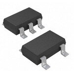
| 描述 | IC REG LDO 3V 0.15A TSOT23-5线性稳压器 150mA Low Quiescent Crnt CMOS |
| 产品分类 | |
| 品牌 | Analog Devices |
| 产品手册 | |
| 产品图片 |
|
| rohs | 符合RoHS无铅 / 符合限制有害物质指令(RoHS)规范要求 |
| 产品系列 | 电源管理 IC,线性稳压器,Analog Devices ADP121-AUJZ30R7- |
| 数据手册 | |
| 产品型号 | ADP121-AUJZ30R7 |
| 产品培训模块 | http://www.digikey.cn/PTM/IndividualPTM.page?site=cn&lang=zhs&ptm=13083 |
| 产品目录页面 | |
| 产品种类 | |
| 供应商器件封装 | TSOT-5 |
| 其它名称 | ADP121-AUJZ30R7CT |
| 包装 | 剪切带 (CT) |
| 商标 | Analog Devices |
| 安装类型 | 表面贴装 |
| 安装风格 | SMD/SMT |
| 封装 | Reel |
| 封装/外壳 | SOT-23-5 细型,TSOT-23-5 |
| 封装/箱体 | TSOT-5 |
| 工作温度 | -40°C ~ 125°C |
| 工厂包装数量 | 3000 |
| 最大工作温度 | + 125 C |
| 最大输入电压 | 5.5 V |
| 最小工作温度 | - 40 C |
| 最小输入电压 | 2.5 V |
| 标准包装 | 1 |
| 电压-跌落(典型值) | 0.12V @ 150mA |
| 电压-输入 | 最高 5.5V |
| 电压-输出 | 3V |
| 电流-输出 | 150mA |
| 电流-限制(最小值) | 160mA |
| 稳压器拓扑 | 正,固定式 |
| 稳压器数 | 1 |
| 系列 | ADP121 |
| 视频文件 | http://www.digikey.cn/classic/video.aspx?PlayerID=1364138032001&width=640&height=505&videoID=2245193149001 |
| 设计资源 | |
| 负载调节 | 10 nV |
| 输出电流 | 150 mA |
| 配用 | /product-detail/zh/ADP121-3.0-EVALZ/ADP121-3.0-EVALZ-ND/1938213 |


- 商务部:美国ITC正式对集成电路等产品启动337调查
- 曝三星4nm工艺存在良率问题 高通将骁龙8 Gen1或转产台积电
- 太阳诱电将投资9.5亿元在常州建新厂生产MLCC 预计2023年完工
- 英特尔发布欧洲新工厂建设计划 深化IDM 2.0 战略
- 台积电先进制程称霸业界 有大客户加持明年业绩稳了
- 达到5530亿美元!SIA预计今年全球半导体销售额将创下新高
- 英特尔拟将自动驾驶子公司Mobileye上市 估值或超500亿美元
- 三星加码芯片和SET,合并消费电子和移动部门,撤换高东真等 CEO
- 三星电子宣布重大人事变动 还合并消费电子和移动部门
- 海关总署:前11个月进口集成电路产品价值2.52万亿元 增长14.8%


PDF Datasheet 数据手册内容提取
150 mA, Low Quiescent Current, CMOS Linear Regulator Data Sheet ADP121 FEATURES TYPICAL APPLICATION CIRCUITS Input voltage range: 2.3 V to 5.5 V Output voltage range: 1.2 V to 3.3 V VIN = 2.3V VOUT = 1.8V 1 VIN VOUT 5 Output current: 150 mA CIN COUT Low quiescent current 1µF 2 GND 1µF I = 11 μA with 0 μA load GND LoIwGN sDh =u 3td0o μwAn w ciuthrr e1n5t0: m<1A μ lAoa d OFFON N3C E= NNO CONNNCEC4T 06901-001 Low dropout voltage Figure 1. ADP121 TSOT with Fixed Output Voltage, 1.8 V 90 mV @ 150 mA load High PSRR 70 dB @ 1 kHz at VOUT = 1.2 V VIN = 2.3V VOUT = 1.8V 70 dB @ 10 kHz at V = 1.2 V VIN VOUT OUT CIN COUT Low noise: 40 μV rms at V = 1.2 V 1µF 1µF OUT No noise bypass capacitor required OStuatbplue tw viothlt aag sem aaclcl u1r μaFcy c:e ±ra1m%i c output capacitor OFFON EN GND 06901-002 Figure 2. ADP121 WLCSP with Fixed Output Voltage, 1.8 V Current limit and thermal overload protection Logic controlled enable 5-lead TSOT package 4-ball 0.4 mm pitch WLCSP APPLICATIONS Mobile phones Digital cameras and audio devices Portable and battery-powered equipment Post dc-to-dc regulation Post regulation GENERAL DESCRIPTION The ADP121 is a quiescent current, low dropout, linear regulator The ADP121 is available in output voltages ranging from 1.2 V that operates from 2.3 V to 5.5 V and provides up to 150 mA of to 3.3 V. The parts are optimized for stable operation with small output current. The low 135 mV dropout voltage at 150 mA 1 μF ceramic output capacitors. The ADP121 delivers good load improves efficiency and allows operation over a wide transient performance with minimal board area. input voltage range. The low 30 μA of quiescent current at full Short-circuit protection and thermal overload protection circuits load makes the ADP121 ideal for battery-operated portable prevent damage in adverse conditions. The ADP121 is available equipment. in a tiny 5-lead TSOT and 4-ball 0.4 mm pitch halide-free WLCSP packages and utilizes the smallest footprint solution to meet a variety of portable applications. Rev. G Information furnished by Analog Devices is believed to be accurate and reliable. However, no responsibility is assumed by Analog Devices for its use, nor for any infringements of patents or other One Technology Way, P.O. Box 9106, Norwood, MA 02062-9106, U.S.A. rights of third parties that may result from its use. Specifications subject to change without notice. No license is granted by implication or otherwise under any patent or patent rights of Analog Devices. Tel: 781.329.4700 www.analog.com Trademarks and registered trademarks are the property of their respective owners. Fax: 781.461.3113 ©2008–2012 Analog Devices, Inc. All rights reserved.
ADP121 Data Sheet TABLE OF CONTENTS Features .............................................................................................. 1 Typical Performance Characteristics ..............................................7 Applications ....................................................................................... 1 Theory of Operation ...................................................................... 11 Typical Application Circuits ............................................................ 1 Applications Information .............................................................. 12 General Description ......................................................................... 1 Capacitor Selection .................................................................... 12 Revision History ............................................................................... 2 Undervoltage Lockout ............................................................... 13 Specifications ..................................................................................... 3 Enable Feature ............................................................................ 13 Recommended Specifications: Input and Output Capacitors 4 Current Limit and Thermal Overload Protection ................. 14 Absolute Maximum Ratings ............................................................ 5 Thermal Considerations ............................................................ 14 Thermal Data ................................................................................ 5 PCB Layout Considerations ...................................................... 17 Thermal Resistance ...................................................................... 5 Outline Dimensions ....................................................................... 18 ESD Caution .................................................................................. 5 Ordering Guide .......................................................................... 19 Pin Configurations and Function Descriptions ........................... 6 REVISION HISTORY 8/12—Rev. F to Rev. G Changes to Table 3 ............................................................................. 5 Changes to Figure 46 Caption and Figure 47 Caption .............. 17 Change to Ordering Guide ............................................................. 19 Changes to Ordering Guide .......................................................... 19 7/12—Rev. E to Rev. F 9/09—Rev. A to Rev. B Updated Outline Dimensions ........................................................ 18 Updated Outline Dimensions ....................................................... 18 Change to Ordering Guide ............................................................. 19 Changes to Ordering Guide .......................................................... 19 8/11—Rev. D to Rev. E 3/09—Rev. 0 to Rev. A Changes to Figure 22 ........................................................................ 9 Changes to Features and General Description Sections .............. 1 Changes to Ordering Guide .......................................................... 19 Changes to Input and Output Capacitor Parameter ..................... 4 1/10—Rev. C to Rev. D Changes to Figure 17 to Figure 20 ................................................... 9 Changes to Ordering Guide .......................................................... 19 Changes to Figure 49 ...................................................................... 17 Added Figure 50 ............................................................................. 17 11/09—Rev. B to Rev. C Changes to Ordering Guide .......................................................... 19 Changes to Figure 1, Figure 2, and General Description 7/08—Revision 0: Initial Version Section ................................................................................................ 1 Rev. G | Page 2 of 20
Data Sheet ADP121 SPECIFICATIONS V = (V + 0.5 V) or 2.3 V, whichever is greater; EN = V ; I = 10 mA; C = C = 1 µF; T = 25°C, unless otherwise noted. IN OUT IN OUT IN OUT A Table 1. Parameter Symbol Conditions Min Typ Max Unit INPUT VOLTAGE RANGE V T = −40°C to +125°C 2.3 5.5 V IN J OPERATING SUPPLY CURRENT I I = 0 µA 11 µA GND OUT I = 0 µA, T = −40°C to +125°C 21 µA OUT J I = 10 mA 15 µA OUT I = 10 mA, T = −40°C to +125°C 29 µA OUT J I = 150 mA 30 µA OUT I = 150 mA, T = −40°C to +125°C 40 µA OUT J SHUTDOWN CURRENT I EN = GND 0.1 µA GND-SD EN = GND, T = −40°C to +125°C 1.5 µA J FIXED OUTPUT VOLTAGE ACCURACY V I = 10 mA −1 +1 % OUT OUT 100 µA < I < 150 mA, −2 +2 % OUT V = (V + 0.5 V) to 5.5 V IN OUT 100 µA < I < 150 mA, −3 +3 % OUT V = (V + 0.5 V) to 5.5 V IN OUT T = −40°C to +125°C J REGULATION Line Regulation ∆V /∆V V = (V + 0.5 V) to 5.5 V, I = 1 mA −0.03 +0.03 %/V OUT IN IN OUT OUT T = −40°C to +125°C J Load Regulation1 ∆V /∆I I = 1 mA to 150 mA 0.001 %/mA OUT OUT OUT I = 1 mA to 150 mA 0.005 %/mA OUT T = −40°C to +125°C J DROPOUT VOLTAGE2 V V = 3.3 V DROPOUT OUT TSOT I = 10 mA 8 mV OUT I = 10 mA, T = −40°C to +125°C 12 mV OUT J I = 150 mA 120 mV OUT I = 150 mA, T = −40°C to +125°C 180 mV OUT J WLCSP I = 10 mA 6 mV OUT I = 10 mA, T = −40°C to +125°C 9 mV OUT J I = 150 mA 90 mV OUT I = 150 mA, T = −40°C to +125°C 135 mV OUT J START-UP TIME3 T V = 3.3 V 120 µs START-UP OUT CURRENT-LIMIT THRESHOLD4 I 160 225 350 mA LIMIT THERMAL SHUTDOWN Thermal Shutdown Threshold TS T rising 150 °C SD J Thermal Shutdown Hysteresis TS 15 °C SD-HYS EN INPUT EN Input Logic High V 2.3 V ≤ V ≤ 5.5 V 1.2 V IH IN EN Input Logic Low V 2.3 V ≤ V ≤ 5.5 V 0.4 V IL IN EN Input Leakage Current V EN = VIN or GND 0.05 µA I-LEAKAGE EN = VIN or GND, T = −40°C to +125°C 1 J UNDERVOLTAGE LOCKOUT UVLO Input Voltage Rising UVLO 2.25 V RISE Input Voltage Falling UVLO 1.5 V FALL Hysteresis UVLO 120 mV HYS OUTPUT NOISE OUT 10 Hz to 100 kHz, V = 5 V, V = 3.3 V 65 µV rms NOISE IN OUT 10 Hz to 100 kHz, V = 5 V, V = 2.5 V 52 µV rms IN OUT 10 Hz to 100 kHz, V = 5 V, V = 1.2 V 40 µV rms IN OUT Rev. G | Page 3 of 20
ADP121 Data Sheet Parameter Symbol Conditions Min Typ Max Unit POWER SUPPLY REJECTION RATIO PSRR 10 kHz, V = 5 V, V = 3.3 V 60 dB IN OUT 10 kHz, V = 5 V, V = 2.5 V 66 dB IN OUT 10 kHz, V = 5 V, V = 1.2 V 70 dB IN OUT 1 Based on an end-point calculation using 1 mA and 100 mA loads. See Figure 6 for typical load regulation performance for loads less than 1 mA. 2 Dropout voltage is defined as the input-to-output voltage differential when the input voltage is set to the nominal output voltage. This applies only for output voltages above 2.3 V. 3 Start-up time is defined as the time between the rising edge of EN to VOUT being at 90% of its nominal value. 4 Current-limit threshold is defined as the current at which the output voltage drops to 90% of the specified typical value. For example, the current limit for a 3.0 V output voltage is defined as the current that causes the output voltage to drop to 90% of 3.0 V, or 2.7 V. RECOMMENDED SPECIFICATIONS: INPUT AND OUTPUT CAPACITORS Table 2. Parameter Symbol Conditions Min Typ Max Unit INPUT AND OUTPUT CAPACITOR1 Minimum Input and Output Capacitance C T = −40°C to +125°C 0.70 µF MIN A Capacitor ESR R T = −40°C to +125°C 0.001 1 Ω ESR A 1 The minimum input and output capacitance should be greater than 0.70 μF over the full range of operating conditions. The full range of operating conditions in the application must be considered during device selection to ensure that the minimum capacitance specification is met. X7R and X5R type capacitors are recommended; Y5V and Z5U capacitors are not recommended for use with any LDO. Rev. G | Page 4 of 20
Data Sheet ADP121 ABSOLUTE MAXIMUM RATINGS Junction-to-ambient thermal resistance, θ , is based on JA Table 3. modeling and calculation using a four-layer board. The Parameter Rating junction-to-ambient thermal resistance is highly dependent VIN to GND −0.3 V to +6.5 V on the application and board layout. In applications where high VOUT to GND −0.3 V to VIN maximum power dissipation exists, close attention to thermal EN to GND −0.3 V to +6.5 V board design is required. The value of θ may vary, depending JA Storage Temperature Range −65°C to +150°C on PCB material, layout, and environmental conditions. The Operating Junction Temperature Range −40°C to +125°C specified values of θ are based on a 4-layer, 4” × 3”, circuit JA Soldering Conditions JEDEC J-STD-020 board. Refer to JESD 51-7 and JESD 51-9 for detailed information on the board construction. For additional Stresses above those listed under Absolute Maximum Ratings information, see AN-617 Application Note, MicroCSPTM may cause permanent damage to the device. This is a stress Wafer Level Chip Scale Package. rating only; functional operation of the device at these or any Ψ is the junction-to-board thermal characterization parameter other conditions above those indicated in the operational JB measured in °C/W. Ψ is based on modeling and calculation section of this specification is not implied. Exposure to absolute JB using a four-layer board. The JESD51-12 Guidelines for Reporting maximum rating conditions for extended periods may affect and Using Package Thermal Information states that thermal device reliability. characterization parameters are not the same as thermal THERMAL DATA resistances. Ψ measures the component power flowing JB Absolute maximum ratings apply individually only, not in through multiple thermal paths rather than a single path as in combination. The ADP121 can be damaged when the junction thermal resistance, θJB. Therefore, ΨJB thermal paths include temperature limits are exceeded. Monitoring the ambient convection from the top of the package as well as radiation temperature does not guarantee that the junction temperature from the package, factors that make ΨJB more useful in real- (TJ) is within the specified temperature limits. In applications world applications. Maximum TJ is calculated from the board with high power dissipation and poor thermal resistance, the temperature (TB) and PD using the following formula: maximum ambient temperature may have to be derated. T = T + (P × Ψ ) J B D JB In applications with moderate power dissipation and low PCB Refer to JESD51-8 and JESD51-12 for more detailed thermal resistance, the maximum ambient temperature can information about Ψ . JB exceed the maximum limit as long as the junction temperature is within specification limits. T of the device is dependent on THERMAL RESISTANCE J the ambient temperature (T ), the power dissipation of the A θ and Ψ are specified for the worst-case conditions, that is, a device (P ), and the junction-to-ambient thermal resistance of JA JB D device soldered in a circuit board for surface-mount packages. the package (θ ). T is calculated from T and P using the JA J A D following formula: Table 4. Thermal Resistance TJ = TA + (PD × θJA) Package Type θJA ΨJB Unit 5-Lead TSOT 170 43 °C/W 4-Ball 0.4 mm Pitch WLCSP 260 58 °C/W ESD CAUTION Rev. G | Page 5 of 20
ADP121 Data Sheet PIN CONFIGURATIONS AND FUNCTION DESCRIPTIONS 1 2 VIN 1 5 VOUT A VIN VOUT TOP VIEW GND 2 (Not to Scale) TOP VIEW (Not to Scale) EN N3C = NO CONNECT4 NC 06901-003 B EN GND 06901-004 Figure 3. 5-Lead TSOT Pin Configuration Figure 4. 4-Ball WLCSP Pin Configuration Table 5. Pin Function Descriptions Pin No. TSOT WLCSP Mnemonic Description 1 A1 VIN Regulator Input Supply. Bypass VIN to GND with a 1 µF or larger capacitor. 2 B2 GND Ground. 3 B1 EN Enable Input. Drive EN high to turn on the regulator; drive EN low to turn off the regulator. For automatic startup, connect EN to VIN. 4 N/A NC No Connect. Not connected internally. 5 A2 VOUT Regulated Output Voltage. Bypass VOUT to GND with a 1 µF or greater capacitor. Rev. G | Page 6 of 20
Data Sheet ADP121 TYPICAL PERFORMANCE CHARACTERISTICS V = 2.3 V, V = 1.8 V, I = 10 mA, C = C = 1 µF, T = 25°C, unless otherwise noted. IN OUT OUT IN OUT A 1.804 40 VOUT = 1.8V VOUT = 1.8V 1.802 VIN = 2.3V 35 VIN = 2.3V 1.800 A) 30 µ 1.798 NT ( 25 V)1.796 RE V (OUT1.794 D CUR 20 N 111...777998208 IIIIIILLLLLLOOOOOOAAAAAADDDDDD ====== 11111100m005µ0m00AµmmAAAAA GROU 11505 IIIIIILLLLLLOOOOOOAAAAAADDDDDD ====== 11111100m005µ0m00AµmmAAAAA 1.786 –40°C –5°C T2J5 °(°CC) 85°C 125°C 06901-005 0 –40°C –5°C T2J5 °(°CC) 85°C 125°C 06901-008 Figure 5. Output Voltage vs. Junction Temperature Figure 8. Ground Current vs. Junction Temperature 1.806 35 VOUT = 1.8V VOUT = 1.8V 1.804 VTAIN == 225.°3CV 30 VTAIN == 225.°3CV A) 25 1.802 T (µ N V) RE 20 (OUT1.800 CUR V D 15 N U 1.798 O GR 10 1.796 5 1.7904.001 0.01 0.1 ILOAD1 (mA) 10 100 100006901-006 00.001 0.01 0.1 ILOAD1 (mA) 10 100 1000 06901-009 Figure 6. Output Voltage vs. Load Current Figure 9. Ground Current vs. Load Current 1.806 35 VOUT = 1.8V ILOAD = 10µA VOUT = 1.8V 1.804 TA = 25°C IILLOOAADD == 110m0AµA 30 TA = 25°C ILOAD = 10mA ILOAD = 50mA A) 25 1.802 ILOAD = 100mA T (µ N V) RE 20 (UT1.800 UR O C V D 15 N U 1.798 GRO 10 IILLOOAADD == 1100µ0µAA ILOAD = 1mA 1.796 5 ILOAD = 10mA ILOAD = 100mA 1.7942.3 2.7 3.1 3.5 VI3N. 9(V) 4.3 4.7 5.1 5.506901-007 02.3 2.7 3.1 3.5 VI3N. 9(V) 4.3 4.I7LOAD =5 .1150mA5.506901-010 Figure 7. Output Voltage vs. Input Voltage Figure 10. Ground Current vs. Input Voltage Rev. G | Page 7 of 20
ADP121 Data Sheet 0.35 140 VIN = 2.30 TA = 25°C 0.30 VVIINN == 23..5000 120 A) VIN = 3.50 WN CURRENT (µ000...221505 VVIINN == 45..2500 (mV)ROPOUT1086000 O D TD V VOUT = 2.5V HU0.10 40 S VOUT = 3.3V 0.05 20 0–50 –25 0 TE2M5PERAT5U0RE (°C7)5 100 125 06901-011 01 10 ILOAD (mA) 100 1000 06901-012 Figure 11. Shutdown Current vs. Temperature at Various Input Voltages Figure 14. Dropout Voltage vs. Load Current, WLCSP 3.35 180 VOUT = 3.3V TA = 25°C TA = 25°C 160 3.30 140 3.25 120 V) V) (mOUT100 V (OUT3.20 VDROP 80 VOUT = 2.5V 3.15 VVOOUUTT @@ 11m0mAA 60 VOUT @ 20mA 40 VOUT = 3.3V 3.10 VVOOUUTT @@ 5100m0mAA VOUT @ 150mA 20 01 10 ILOAD (mA) 100 1000 06901-018 3.035.20 3.25 3.30 3.35 V3IN.4 (0V) 3.45 3.50 3.55 3.6006901-013 Figure 12. Dropout Voltage vs. Load Current, TSOT Figure 15. Output Voltage vs. Input Voltage (In Dropout), WLCSP 3.35 60 VOUT = 3.3V VOUT = 3.3V TA = 25°C TA = 25°C 3.30 50 A) 3.25 T (µ40 N V) RE (OUT3.20 CUR30 V D N 3.15 VVOOUUTT @@ 11m0mAA ROU20 VOUT @ 20mA G 3.10 VVVOOOUUUTTT @@@ 511005m00mmAAA 10 IIILLLOOOAAADDD === 112m00mmAAA IIILLLOOOAAADDD === 511005m00mmAAA 3.035.20 3.25 3.30 3.35 V3IN.4 (0V) 3.45 3.50 3.55 3.6006901-019 30.20 3.25 3.30 3.35 V3IN.4 (0V) 3.45 3.50 3.55 3.60 06901-020 Figure 13. Output Voltage vs. Input Voltage (In Dropout), TSOT Figure 16. Ground Current vs. Input Voltage (In Dropout) Rev. G | Page 8 of 20
Data Sheet ADP121 0 0 VRIPPLE = 50mV 3.3V/150mA 1.2V/150mA 1.8V/150mA –10 VIN = 5V 3.3V/100µA 1.2V/100µA 1.8V/100µA VOUT = 1.2V –20 –20 COUT = 1µF 150mA –30 100mA –40 10mA B) –40 1mA B) RR (d –50 100µ0AµA RR (d –60 S S P –60 P –80 –70 –80 –100 –90 –10010 100 1kFREQU1E0NkCY (Hz)100k 1M 10M06901-014 –12010 100 1kFREQU1E0NkCY (Hz)100k 1M 10M06901-017 Figure 17. Power Supply Rejection Ratio vs. Frequency Figure 20. Power Supply Rejection Ratio vs. Frequency at Various Output Voltages and Load Currents 0 10 ––1200 VVCVRIOONIUUP =TTP L5==EV 11 =.µ8 F5V0mV 11150000mmmAAA 113...283VVV 1mA –30 100µA 1 B) –40 0µA √Hz) RR (d –50 E (µV/ S S P –60 OI N 0.1 –70 –80 –90 –10010 100 1kFREQU1E0NkCY (Hz)100k 1M 10M06901-015 010 100 FREQUE1NkCY (Hz) 10k 100k 06901-021 Figure 18. Power Supply Rejection Ratio vs. Frequency Figure 21. Output Noise Spectrum, V = 5 V, I = 10 mA, C = 1 µF IN LOAD OUT 0 70 VRIPPLE = 50mV ––1200 VCVIOONUU =TT 5==V 31.µ3FV 1111500m00mAmmAAA 60 –30 100µ0AµA ms) 50 PSRR (dB) –––456000 T (µV rNOISE4300 U O –70 20 3.3V 2.5V –80 1.8V 10 1.5V –90 1.2V –10010 100 1kFREQU1E0NkCY (Hz)100k 1M 10M06901-016 00.001 0.01 0.1 ILOAD1 (mA) 10 100 1000 06901-022 Figure 19. Power Supply Rejection Ratio vs. Frequency Figure 22. Output Noise vs. Load Current and Output Voltage, V = 5 V, C = 1 μF IN OUT Rev. G | Page 9 of 20
ADP121 Data Sheet VIN V) 1mA TO 150mA LOAD STEP, ILOAD DI 2.5A/µs V) A/ DI 4V TO 5V INPUT VOLTAGE STEP, m V/ 2V/µs 150 (1 ( VOUT DIV) DIV) VOUT V/ V/ m m (50 VIN = 5V (10 VOUT = 1.8V, (40µs/DIV) VOUT = 1.8V 06901-024 CIN = COUT = 1µF (4µs/DIV) 06901-037 Figure 23. Load Transient Response, C = C = 1 μF Figure 25. Line Transient Response, Load Current = 150 mA IN OUT VOUT = 1.8V, V) 1mA TO 150mA LOAD STEP, ILOAD CIN = COUT = 1µF DI 2.5A/µs V) VIN A/ DI m V/ (150 (1 4V TO 5V INPU2TV /VµOsLTAGE STEP, V) VOUT V) DI DI VOUT V/ V/ m m (50 VIN = 5V (10 (40µs/DIV) VOUT = 1.8V 06901-025 (10µs/DIV) 06901-038 Figure 24. Load Transient Response, C = C = 4.7 μF Figure 26. Line Transient Response, Load Current = 1 mA IN OUT Rev. G | Page 10 of 20
Data Sheet ADP121 THEORY OF OPERATION The ADP121 is a low quiescent current, low dropout linear Internally, the ADP121 consists of a reference, an error amplifier, regulator that operates from 2.3 V to 5.5 V and provides up a feedback voltage divider, and a PMOS pass transistor. Output to 150 mA of output current. Drawing a low 30 μA quiescent current is delivered via the PMOS pass device, which is con- current (typical) at full load makes the ADP121 ideal for battery- trolled by the error amplifier. The error amplifier compares the operated portable equipment. Shutdown current consumption reference voltage with the feedback voltage from the output and is typically 100 nA. amplifies the difference. If the feedback voltage is lower than the reference voltage, the gate of the PMOS device is pulled Optimized for use with small 1 µF ceramic capacitors, lower, allowing more current to flow and increasing the output the ADP121 provides excellent transient performance. voltage. If the feedback voltage is higher than the reference voltage, the gate of the PMOS device is pulled higher, allowing VIN VOUT less current to flow and decreasing the output voltage. R1 The ADP121 is available in output voltages ranging from 1.2 V to GND SHORT CIRCUIT, 3.3 V. The ADP121 uses the EN pin to enable and disable the UVLO, AND THERMAL VOUT pin under normal operating conditions. When EN is PROTECT high, VOUT turns on; when EN is low, VOUT turns off. For automatic startup, EN can be tied to VIN. EN SHUTDOWN 0.8V REFERENCE R2 06901-023 Figure 27. Internal Block Diagram Rev. G | Page 11 of 20
ADP121 Data Sheet APPLICATIONS INFORMATION CAPACITOR SELECTION Input Bypass Capacitor Output Capacitor Connecting a 1 µF capacitor from VIN to GND reduces the circuit sensitivity to the PCB layout, especially when long input The ADP121 is designed for operation with small, space-saving traces or high source impedance is encountered. If output ceramic capacitors, but functions with most commonly used capacitance greater than 1 µF is required, the input capacitor capacitors as long as care is taken with the effective series resistance should be increased to match it. (ESR) value. The ESR of the output capacitor affects stability of the LDO control loop. A minimum of 0.70 µF capacitance with an Input and Output Capacitor Properties ESR of 1 Ω or less is recommended to ensure stability of the Any good quality ceramic capacitor can be used with the ADP121. The transient response to changes in the load current is ADP121, as long as it meets the minimum capacitance and also affected by output capacitance. Using a larger value of output maximum ESR requirements. Ceramic capacitors are manufac- capacitance improves the transient response of the ADP121 to tured with a variety of dielectrics, each with a different behavior large changes in the load current. Figure 28 and Figure 29 show over temperature and applied voltage. Capacitors must have an the transient responses for output capacitance values of 1 µF and adequate dielectric to ensure the minimum capacitance over 4.7 µF, respectively. the necessary temperature range and dc bias conditions. X5R or X7R dielectrics with a voltage rating of 6.3 V or 10 V are ILOAD recomm ended. Y5V and Z5U dielectrics are not recommended, due to their poor temperature and dc bias V) 1mA TO 150mA LOAD STEP, DI 2.5A/µs characteristics. A/ m 50 CH1 MEAN Figure 30 depicts the capacitance vs. voltage bias characteristic (1 115.7mA of an 0402 1 µF, 10 V, X5R capacitor. The voltage stability of a capacitor is strongly influenced by the capacitor size and voltage rating. In general, a capacitor in a larger package or higher voltage V) rating exhibits better stability. The temperature variation of the DI V/ X5R dielectric is about ±15% over the −40°C to +85°C tempera- m (50 VOUT = 1.8V, VOUT ture range and is not a function of package or voltage rating. CIN = COUT = 1µF (400ns/DIV) 06901-039 1.2 1.0 Figure 28. Output Transient Response, C = 1 µF OUT F) 0.8 µ E ( ILOAD NC A 0.6 DIV) 1mA TO 1520.m5AA/ µLsOAD STEP, ACIT 0mA/ CAP 0.4 5 1 ( 0.2 V/DIV) VOUT 00 2 V4OLTAGE (V6) 8 1006901-036 m Figure 30. Capacitance vs. Voltage Bias Characteristic 0 5 ( VOUT = 1.8V, CIN = COUT = 4.7µF (400ns/DIV) 06901-040 Figure 29. Output Transient Response, C = 4.7 µF OUT Rev. G | Page 12 of 20
Data Sheet ADP121 Equation 1 can be used to determine the worst-case capacitance As shown in Figure 31, the EN pin has built in hysteresis. This accounting for capacitor variation over temperature, compo- prevents on/off oscillations that may occur due to noise on the nent tolerance, and voltage. EN pin as it passes through the threshold points. C = C × (1 − TEMPCO) × (1 − TOL) (1) The active/inactive thresholds of the EN pin are derived from EFF BIAS the VIN voltage. Therefore, these thresholds vary with changing where: input voltage. Figure 32 shows typical EN active/inactive C is the effective capacitance at the operating voltage. BIAS thresholds when the input voltage varies from 2.3 V to 5.5 V. TEMPCO is the worst-case capacitor temperature coefficient. TOL is the worst-case component tolerance. 1.10 In this example, TEMPCO over −40°C to +85°C is assumed to 1.05 be 15% for an X5R dielectric. TOL is assumed to be 10%, and V) C is 0.94 μF at 1.8 V from the graph in Figure 30. DS (1.00 BIAS L EN ACTIVE Substituting these values in Equation 1 yields SHO0.95 E R CEFF = 0.94 μF × (1 − 0.15) × (1 − 0.1) = 0.719 μF N TH0.90 E Therefore, the capacitor chosen in this example meets the L 0.85 A minimum capacitance requirement of the LDO over YPIC0.80 EN INACTIVE temperature and tolerance at the chosen output voltage. T 0.75 To guarantee the performance of the ADP121, it is imperative tbheahta tvhieo re foffe cthtse ocfa dpac cbitiaosr,s taerme peevraalutuartee,d a fnodr etoalcehr aanpcpelsic oanti othne. 0.720.252.502.753.003.253.503.V7I5N 4(V.0)04.254.504.755.005.255.50 06901-027 UNDERVOLTAGE LOCKOUT Figure 32. Typical EN Pin Thresholds vs. Input Voltage The ADP121 has an internal undervoltage lockout circuit that The ADP121 utilizes an internal soft start to limit the inrush disables all inputs and the output when the input voltage is less current when the output is enabled. The start-up time for the than approximately 2.2 V. This ensures that the inputs of the 1.8 V option is approximately 120 µs from the time the EN ADP121 and the output behave in a predictable manner during active threshold is crossed to when the output reaches 90% of its power-up. final value. The start-up time is somewhat dependant on the output voltage setting and increases slightly as the output ENABLE FEATURE voltage increases. The ADP121 uses the EN pin to enable and disable the VOUT 6 pin under normal operating conditions. Figure 31 shows a EN rising voltage on EN crossing the active threshold, and then 5 VOUT turns on. When a falling voltage on EN crosses the inactive threshold, VOUT turns off. 4 V) VVIONU =T 5=V 1.8V VOLTS ( 3 3.3V CILIONA =D C=O 1U0T0 m= A1µF VOUT 2 1.8V 1 V 1.2V V/DI EN m 500 00 20 40 60 80 TIM1E00 (µs)120 140 160 180 200 06901-041 Figure 33. Typical Start-Up Time 40ms/DIV 06901-026 Figure 31. ADP121 Typical EN Pin Operation Rev. G | Page 13 of 20
ADP121 Data Sheet CURRENT LIMIT AND THERMAL OVERLOAD dissipation in the power device, and thermal resistances between PROTECTION the junction-and-ambient air (θ ). The θ number is dependent JA JA on the package assembly compounds used and the amount of The ADP121 is protected against damage due to excessive copper to which the GND pins of the package are soldered on the power dissipation by current and thermal overload protection PCB. Table 6 shows typical θ values for various PCB copper circuits. The ADP121 is designed to current limit when the JA sizes and Table 7 shows the typical Ψ values for the ADP121. output load reaches 225 mA (typical). When the output load JB exceeds 225 mA, the output voltage is reduced to maintain a Table 6. Typical θ Values JA constant current limit. Copper Size (mm2) TSOT (°C/W) WLCSP (°C/W) Thermal overload protection is built-in, which limits the 01 170 260 junction temperature to a maximum of 150°C (typical). Under 50 152 159 extreme conditions (that is, high ambient temperature and 100 146 157 power dissipation) when the junction temperature starts to 300 134 153 rise above 150°C, the output is turned off, reducing the output 500 131 151 current to zero. When the junction temperature drops below 1 Device soldered to minimum size pin traces. 135°C, the output is turned on again and output current is restored to its nominal value. Table 7. Typical Ψ Values JB Consider the case where a hard short from VOUT to GND occurs. TSOT (°C/W) WLCSP (°C/W) At first, the ADP121 current limits, so that only 225 mA is con- 42.8 58.4 ducted into the short. If self-heating of the junction is great The junction temperature of the ADP121 can be calculated enough to cause its temperature to rise above 150°C, thermal from the following equation: shutdown activates turning off the output and reducing the output current to zero. As the junction temperature cools and T = T + (P × θ ) (2) J A D JA drops below 135°C, the output turns on and conducts 225 mA where: into the short, again causing the junction temperature to rise T is the ambient temperature. A above 150°C. This thermal oscillation between 135°C and P is the power dissipation in the die, given by D 150°C causes a current oscillation between 225 mA and 0 mA P = [(V − V ) × I ] + (V × I ) (3) that continues as long as the short remains at the output. D IN OUT LOAD IN GND where: Current and thermal limit protections are intended to protect I is the load current. the device against accidental overload conditions. For reliable LOAD I is the ground current. operation, device power dissipation must be externally limited GND V and V are input and output voltages, respectively. so junction temperatures do not exceed 125°C. IN OUT THERMAL CONSIDERATIONS Power dissipation due to ground current is quite small and can be ignored. Therefore, the junction temperature equation In most applications, the ADP121 does not dissipate a lot of heat simplifies to due to high efficiency. However, in applications with a high T = T + {[(V − V ) × I ] × θ } (4) ambient temperature and high supply voltage to an output voltage J A IN OUT LOAD JA differential, the heat dissipated in the package is large enough As shown in Equation 4, for a given ambient temperature, that it can cause the junction temperature of the die to exceed input-to-output voltage differential, and continuous load the maximum junction temperature of 125°C. current, there exists a minimum copper size requirement for the PCB to ensure that the junction temperature does not rise When the junction temperature exceeds 150°C, the converter above 125°C. Figure 34 to Figure 47 show junction temperature enters thermal shutdown. It recovers only after the junction calculations for different ambient temperatures, load currents, temperature has decreased below 135°C to prevent any permanent V -to-V differentials, and areas of PCB copper. damage. Therefore, thermal analysis for the chosen application IN OUT is very important to guarantee reliable performance over all In cases where the board temperature is known, the thermal conditions. The junction temperature of the die is the sum of characterization parameter, Ψ , can be used to estimate the JB the ambient temperature of the environment and the tempera- junction temperature rise. T is calculated from T and P using J B D ture rise of the package due to the power dissipation, as shown the formula in Equation 2. T = T + (P × Ψ ) (5) J B D JB To guarantee reliable operation, the junction temperature of the ADP121 must not exceed 125°C. To ensure that the junction temperature stays below this maximum value, the user needs to be aware of the parameters that contribute to junction temperature changes. These parameters include ambient temperature, power Rev. G | Page 14 of 20
Data Sheet ADP121 140 140 MAX JUNCTION TEMPERATURE MAX JUNCTION TEMPERATURE E, T (°C)J112000 IIIILLLLOOOOAAAADDDD ==== 1251m050mmmAAAA E, T (°C)J112000 RATUR 80 IIILLLOOOAAADDD === 711505m00mmAAA RATUR 80 E E P P M M E 60 E 60 T T N N O O TI 40 TI 40 C C JUN 20 JUN 20 IILLOOAADD == 11m0mAA IILLOOAADD == 7150m0mAA ILOAD = 25mA ILOAD = 150mA ILOAD = 50mA 00.5 1.0 1.5 2.0VIN – V2O.5UT (V)3.0 3.5 4.0 4.506901-028 00.5 1.0 1.5 2.0VIN – V2O.5UT (V)3.0 3.5 4.0 4.506901-031 Figure 34. TSOT, 500 mm2 of PCB Copper, T = 25°C Figure 37. TSOT, 500 mm2 of PCB Copper, T = 50°C A A 140 140 MAX JUNCTION TEMPERATURE MAX JUNCTION TEMPERATURE C)120 ILOAD = 1mA C)120 E, T (°J100 IIILLLOOOAAADDD === 125050mmmAAA E, T (°J100 RATUR 80 IIILLLOOOAAADDD === 1715500m0mmAAA RATUR 80 E E P P M M E 60 E 60 T T N N O O TI 40 TI 40 C C UN UN ILOAD = 1mA ILOAD = 75mA J 20 J 20 ILOAD = 10mA ILOAD = 100mA ILOAD = 25mA ILOAD = 150mA ILOAD = 50mA 00.5 1.0 1.5 2.0VIN – V2O.5UT (V)3.0 3.5 4.0 4.506901-029 00.5 1.0 1.5 2.0VIN – V2O.5UT (V)3.0 3.5 4.0 4.506901-032 Figure 35. TSOT, 100 mm2 of PCB Copper, T = 25°C Figure 38. TSOT, 100 mm2 of PCB Copper, T = 50°C A A 140 140 MAX JUNCTION TEMPERATURE MAX JUNCTION TEMPERATURE C)120 ILOAD = 1mA C)120 E, T (°J100 IIILLLOOOAAADDD === 125050mmmAAA E, T (°J100 RATUR 80 IIILLLOOOAAADDD === 711505m00mmAAA RATUR 80 E E P P M M E 60 E 60 T T N N O O TI 40 TI 40 C C UN UN ILOAD = 1mA ILOAD = 75mA J 20 J 20 ILOAD = 10mA ILOAD = 100mA ILOAD = 25mA ILOAD = 150mA ILOAD = 50mA 00.5 1.0 1.5 2.0VIN – V2O.5UT (V)3.0 3.5 4.0 4.506901-030 00.5 1.0 1.5 2.0VIN – V2O.5UT (V)3.0 3.5 4.0 4.506901-033 Figure 36. TSOT, 0 mm2 of PCB Copper, T = 25°C Figure 39. TSOT, 0 mm2 of PCB Copper, T = 50°C A A Rev. G | Page 15 of 20
ADP121 Data Sheet 140 140 MAX JUNCTION TEMPERATURE MAX JUNCTION TEMPERATURE 120 120 C) ILOAD = 1mA C) URE, T (°J100 IIIILLLLOOOOAAAADDDD ==== 12570505mmmmAAAA URE, T (°J100 AT 80 ILOAD = 100mA AT 80 ER ILOAD = 150mA ER P P M M E 60 E 60 T T N N O O TI 40 TI 40 C C UN UN ILOAD = 1mA ILOAD = 75mA J 20 J 20 ILOAD = 10mA ILOAD = 100mA ILOAD = 25mA ILOAD = 150mA ILOAD = 50mA 00.5 1.0 1.5 2.0VIN – V2O.5UT (V)3.0 3.5 4.0 4.506901-042 00.5 1.0 1.5 2.0VIN – V2O.5UT (V)3.0 3.5 4.0 4.506901-045 Figure 40. WLCSP, 500 mm2 of PCB Copper, T = 25°C Figure 43. WLCSP, 500 mm2 of PCB Copper, T = 50°C A A 140 140 MAX JUNCTION TEMPERATURE MAX JUNCTION TEMPERATURE 120 120 URE, T (°C)J100 IIIIILLLLLOOOOOAAAAADDDDD ===== 11257m0505mmmmAAAAA URE, T (°C)J100 AT 80 ILOAD = 100mA AT 80 ER ILOAD = 150mA ER P P M M E 60 E 60 T T N N O O TI 40 TI 40 C C UN UN ILOAD = 1mA ILOAD = 75mA J 20 J 20 ILOAD = 10mA ILOAD = 100mA ILOAD = 25mA ILOAD = 150mA ILOAD = 50mA 00.5 1.0 1.5 2.0VIN – V2O.5UT (V)3.0 3.5 4.0 4.506901-043 00.5 1.0 1.5 2.0VIN – V2O.5UT (V)3.0 3.5 4.0 4.506901-046 Figure 41. WLCSP, 100 mm2 of PCB Copper, T = 25°C Figure 44. WLCSP, 100 mm2 of PCB Copper, T = 50°C A A 140 140 MAX JUNCTION MAX JUNCTION TEMPERATURE TEMPERATURE 120 120 C) C) E, T (°J100 E, T (°J100 R R U U AT 80 AT 80 R R E E P P M M E 60 E 60 T T N N O O TI 40 TI 40 C C UN UN ILOAD = 1mA ILOAD = 75mA J 20 IIILLLOOOAAADDD === 112m05mmAAA IILLOOAADD == 5705mmAA IILLOOAADD == 110500mmAA J 20 IIILLLOOOAAADDD === 125050mmmAAA IILLOOAADD == 110500mmAA 00.5 1.0 1.5 2.0VIN – V2O.5UT (V)3.0 3.5 4.0 4.506901-044 00.5 1.0 1.5 2.0VIN – V2O.5UT (V)3.0 3.5 4.0 4.506901-047 Figure 42. WLCSP, 0 mm2 of PCB Copper, T = 25°C Figure 45. WLCSP, 0 mm2 of PCB Copper, T = 50°C A A Rev. G | Page 16 of 20
Data Sheet ADP121 140 GND GND MAX JUNCTION TEMPERATURE ANALOGDEVICES ADP121-xx-EVALZ 120 C) RE, T (°J100 C1 C2 ATU 80 U1 R E P TEM 60 IILLOOAADD == 11m0mAA N ILOAD = 25mA CTIO 40 IILLOOAADD == 5705mmAA UN ILOAD = 100mA J 20 ILOAD = 150mA J1 VIN VOUT 00.5 1.0 1.5 2.0VIN – V2O.5UT (V)3.0 3.5 4.0 4.506901-048 Figure 46. TSOT, 100 mm2 of PCB Copper, Board Temperature = 85°C 140 C)120 MAX JUNCTION TEMPERATURE GND EN GND 06901-034 E, T (°J100 Figure 48. Example of TSOT PCB Layout R U AT 80 R E P TEM 60 IILLOOAADD == 11m0mAA CTION 40 IIILLLOOOAAADDD === 257505mmmAAA UN ILOAD = 100mA J 20 ILOAD = 150mA 00.5 1.0 1.5 2.0VIN – V2O.5UT (V)3.0 3.5 4.0 4.506901-049 Figure 47. WLCSP, 100 mm2 of PCB Copper, Board Temperature = 85°C PCB LAYOUT CONSIDERATIONS Htheea atm diosusinpta otifo cno fprpoemr atthtae cphaecdk atog eth cea np ibnes iomf tphreo vAeDd Pb1y2 i1n.c Hreoawsienvge r, 06901-050 Figure 49. Example of WLCSP PCB Layout—Top Side as can be seen from Table 6 and Table 7, a point of diminishing returns is eventually reached, beyond which an increase in the copper size does not yield significant heat dissipation benefits. Place the input capacitor as close as possible to the VIN and GND pins. Place the output capacitor as close as possible to the VOUT and GND pins. Use 0402 or 0603 size capacitors and resistors to achieve the smallest possible footprint solution on boards where area is limited. 06901-051 Figure 50. Example of WLCSP PCB Layout—Bottom Side Rev. G | Page 17 of 20
ADP121 Data Sheet OUTLINE DIMENSIONS 2.90 BSC 5 4 1.60 BSC 2.80 BSC 1 2 3 0.95 BSC 1.90 *0.90 MAX BSC 0.70 MIN *1.00 MAX 0.20 0.08 8° 0.10 MAX 0.50 SEATING 4° 0.60 0.30 PLANE 0° 0.45 0.30 *CTHOEM PELXICAENPTT TIOON J OEDF EPCA CSTKAANGDEA HREDIGS HMTO A-1N9D3 -TAHBICWKINTHESS. 100708-A Figure 51. 5-Lead Thin Small Outline Transistor Package [TSOT] (UJ-5) Dimensions show in millimeters 0.860 0.820 SQ 0.780 2 1 A BALLA1 IDENTIFIER 0.40 B REF TOP VIEW BOTTOM VIEW (BALL SIDE DOWN) (BALL SIDE UP) 0.381 0.660 0.356 0.600 END VIEW 0.331 0.540 COPLANARITY 0.05 SEPALTAINNGE 000...222864000 000...221307000 07-10-2012-A Figure 52. 4-Ball Wafer Level Chip Scale- Package [WLCSP] (CB-4-2) Dimensions show in millimeters Rev. | Page 18 of 20
Data Sheet ADP121 ORDERING GUIDE Temperature Output Package Model1 Range Voltage (V)2 Package Description Option3 Branding ADP121-AUJZ12R7 −40°C to +125°C 1.2 5-Lead TSOT UJ-5 LC0 ADP121-AUJZ15R7 −40°C to +125°C 1.5 5-Lead TSOT UJ-5 LC1 ADP121-AUJZ18R7 −40°C to +125°C 1.8 5-Lead TSOT UJ-5 LC7 ADP121-AUJZ20R7 −40°C to +125°C 2.0 5-Lead TSOT UJ-5 LC9 ADP121-AUJZ25R7 −40°C to +125°C 2.5 5-Lead TSOT UJ-5 LCA ADP121-AUJZ28R7 −40°C to +125°C 2.8 5-Lead TSOT UJ-5 LA3 ADP121-AUJZ30R7 −40°C to +125°C 3.0 5-Lead TSOT UJ-5 LA4 ADP121-AUJZ33R7 −40°C to +125°C 3.3 5-Lead TSOT UJ-5 LA5 ADP121-ACBZ12R7 −40°C to +125°C 1.2 4-Ball WLCSP CB-4-2 LC0 ADP121-ACBZ15R7 −40°C to +125°C 1.5 4-Ball WLCSP CB-4-2 LC1 ADP121-ACBZ165R7 −40°C to +125°C 1.65 4-Ball WLCSP CB-4-2 LC4 ADP121-ACBZ18R7 −40°C to +125°C 1.8 4-Ball WLCSP CB-4-2 LC7 ADP121-ACBZ188R7 −40°C to +125°C 1.875 4-Ball WLCSP CB-4-2 LC8 ADP121-ACBZ20R7 −40°C to +125°C 2.0 4-Ball WLCSP CB-4-2 LC9 ADP121-ACBZ25R7 −40°C to +125°C 2.5 4-Ball WLCSP CB-4-2 LCA ADP121-ACBZ28R7 −40°C to +125°C 2.8 4-Ball WLCSP CB-4-2 LCD ADP121-ACBZ30R7 −40°C to +125°C 3.0 4-Ball WLCSP CB-4-2 LCF ADP121-ACBZ33R7 −40°C to +125°C 3.3 4-Ball WLCSP CB-4-2 LCG ADP121CB-1.2-EVALZ 1.2 ADP121 1.2 V Output Evaluation Board ADP121CB-1.5-EVALZ 1.5 ADP121 1.5 V Output Evaluation Board ADP121CB-1.8-EVALZ 1.8 ADP121-1 1.8 V Output Evaluation Board ADP121CB-2.0-EVALZ 2.0 ADP121-1 2.0 V Output Evaluation Board ADP121CB-2.5-EVALZ 2.5 ADP121-1 2.5 V Output Evaluation Board ADP121CB-2.8-EVALZ 2.8 ADP121-1 2.8 V Output Evaluation Board ADP121CB-3.0-EVALZ 3.0 ADP121-1 3.0 V Output Evaluation Board ADP121CB-3.3-EVALZ 3.3 ADP121-1 3.3 V Output Evaluation Board ADP121UJZ-REDYKIT Evaluation Board Kit 1 Z = RoHS Compliant Part. 2 For additional voltage options, contact your local Analog Devices, Inc., sales or distribution representative. 3 The WLCSP package option is halide free. Rev. G | Page 19 of 20
ADP121 Data Sheet NOTES ©2008–2012 Analog Devices, Inc. All rights reserved. Trademarks and registered trademarks are the property of their respective owners. D06901-0-8/12(G) Rev. G | Page 20 of 20