ICGOO在线商城 > 集成电路(IC) > PMIC - 稳压器 - 线性 > LM317T-DG
 Datasheet下载
- 型号: LM317T-DG
- 制造商: STMicroelectronics
- 库位|库存: xxxx|xxxx
- 要求:
| 数量阶梯 | 香港交货 | 国内含税 |
| +xxxx | $xxxx | ¥xxxx |
查看当月历史价格
查看今年历史价格
LM317T-DG产品简介:
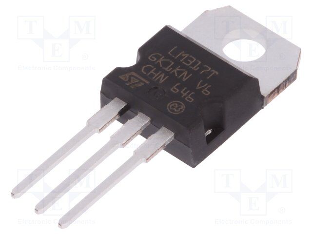
ICGOO电子元器件商城为您提供LM317T-DG由STMicroelectronics设计生产,在icgoo商城现货销售,并且可以通过原厂、代理商等渠道进行代购。 LM317T-DG价格参考¥0.68-¥0.90。STMicroelectronicsLM317T-DG封装/规格:PMIC - 稳压器 - 线性, Linear Voltage Regulator IC 1 Output 1.5A TO-220-3。您可以下载LM317T-DG参考资料、Datasheet数据手册功能说明书,资料中有LM317T-DG 详细功能的应用电路图电压和使用方法及教程。
STMicroelectronics(意法半导体)生产的LM317T-DG是一款经典的三端可调正电压线性稳压器,属于PMIC中的线性稳压器类别。该器件可在1.25V至37V的输出电压范围内连续调节,最大输出电流可达1.5A,具有良好的线路和负载调整率。

LM317T-DG广泛应用于各类需要稳定可调直流电压的电子设备中。常见应用场景包括:
- 电源供应单元:作为实验室电源、适配器或嵌入式系统的可调稳压模块;
- 工业控制设备:为传感器、PLC模块或执行器提供稳定供电;
- 消费类电子产品:用于家电控制板、充电器或LED驱动电路中;
- 通信设备:为射频模块或信号处理电路提供低噪声电源;
- 教育与开发领域:因外围电路简单、使用方便,常用于教学实验板和原型设计。

该器件采用TO-220封装,具备过载保护、过热保护和安全工作区补偿功能,可靠性高,适用于中低功率场景。由于其无需散热片也能在适度负载下良好工作,特别适合空间受限但需稳定电压输出的设计。

总之,LM317T-DG凭借其高稳定性、易用性和宽电压调节范围,成为众多电子系统中理想的线性稳压解决方案。
| 参数 | 数值 |
| 产品目录 | 集成电路 (IC)半导体 |
| 描述 | IC REG LDO ADJ 1.5A TO220-3线性稳压器 Dual Guage ADJ 1.2V to 37V 1.5A |
| 产品分类 | |
| 品牌 | STMicroelectronics |
| 产品手册 | |
| 产品图片 |
|
| rohs | 符合RoHS无铅 / 符合限制有害物质指令(RoHS)规范要求 |
| 产品系列 | 电源管理 IC,线性稳压器,STMicroelectronics LM317T-DG- |
| 数据手册 | |
| 产品型号 | LM317T-DG |
| PSRR/纹波抑制—典型值 | 80 dB |
| 产品种类 | |
| 供应商器件封装 | TO-220-3 |
| 其它名称 | 497-12403 |
| 包装 | 管件 |
| 商标 | STMicroelectronics |
| 安装类型 | 通孔 |
| 安装风格 | Through Hole |
| 封装 | Tube |
| 封装/外壳 | TO-220-3 |
| 封装/箱体 | TO-220 |
| 工作温度 | 0°C ~ 125°C |
| 工厂包装数量 | 50 |
| 最大工作温度 | + 125 C |
| 最大输入电压 | 40 V |
| 最小工作温度 | 0 C |
| 最小输入电压 | 4.2 V |
| 极性 | Positive |
| 标准包装 | 50 |
| 电压-跌落(典型值) | - |
| 电压-输入 | - |
| 电压-输出 | 1.2 V ~ 37 V |
| 电流-输出 | 1.5A |
| 电流-限制(最小值) | - |
| 稳压器拓扑 | 正,可调式 |
| 稳压器数 | 1 |
| 系列 | LM317 |
| 线路调整率 | 0.04 % / V |
| 负载调节 | 0.5 % |
| 输出电压 | 1.2 V to 37 V |
| 输出电流 | 1.5 A |
| 输出端数量 | 1 |
| 输出类型 | Adjustable |


- 商务部:美国ITC正式对集成电路等产品启动337调查
- 曝三星4nm工艺存在良率问题 高通将骁龙8 Gen1或转产台积电
- 太阳诱电将投资9.5亿元在常州建新厂生产MLCC 预计2023年完工
- 英特尔发布欧洲新工厂建设计划 深化IDM 2.0 战略
- 台积电先进制程称霸业界 有大客户加持明年业绩稳了
- 达到5530亿美元!SIA预计今年全球半导体销售额将创下新高
- 英特尔拟将自动驾驶子公司Mobileye上市 估值或超500亿美元
- 三星加码芯片和SET,合并消费电子和移动部门,撤换高东真等 CEO
- 三星电子宣布重大人事变动 还合并消费电子和移动部门
- 海关总署:前11个月进口集成电路产品价值2.52万亿元 增长14.8%


PDF Datasheet 数据手册内容提取
LM217, LM317 Datasheet 1.2 V to 37 V adjustable voltage regulators Features • Output voltage range: 1.2 to 37 V • Output current in excess of 1.5 A • 0.1% line and load regulation • Floating operation for high voltages TO-220 TO-220FP • Complete series of protections: current limiting, thermal shutdown and SOA control Description D²PAK The LM217, LM317 are monolithic integrated circuits in TO-220, TO-220FP and D²PAK packages intended for use as positive adjustable voltage regulators. They are designed to supply more than 1.5 A of load current with an output voltage adjustable over a 1.2 to 37 V range. The nominal output voltage is selected by means of a resistive divider, making the device exceptionally easy to use and eliminating the stocking of many fixed regulators. Product status link LM217 LM317 DS0433 - Rev 21 - July 2019 www.st.com For further information contact your local STMicroelectronics sales office.
LM217, LM317 Pin configuration 1 Pin configuration Figure 1. Pin connections (top view) TO-220 TO-220FP D²PAK DS0433 - Rev 21 page 2/31
LM217, LM317 Maximum ratings 2 Maximum ratings Table 1. Absolute maximum ratings Symbol Parameter Value Unit VI - VO Input-reference differential voltage 40 V IO Output current Internally limited A LM217 - 25 to 150 TOP Operating junction temperature for: LM317 0 to 125 °C LM317B -40 to 125 PD Power dissipation Internally limited TSTG Storage temperature - 65 to 150 °C Note: Absolute maximum ratings are those values beyond which damage to the device may occur. Functional operation under these condition is not implied. Table 2. Thermal data Symbol Parameter D²PAK TO-220 TO-220FP Unit RthJA Thermal resistance junction-ambient 62.5 50 60 °C/W RthJC Thermal resistance junction-case 3 5 5 °C/W DS0433 - Rev 21 page 3/31
LM217, LM317 Diagram 3 Diagram Figure 2. Schematic diagram DS0433 - Rev 21 page 4/31
LM217, LM317 Electrical characteristics 4 Electrical characteristics V - V = 5 V, I = 500 mA, I = 1.5 A and P = 20 W, T = - 25 to 150 °C, unless otherwise specified. I O O MAX MAX J Table 3. Electrical characteristics for LM217 Symbol Parameter Test conditions Min. Typ. Max. Unit TJ = 25°C 0.01 0.02 ΔVO Line regulation VI - VO = 3 to 40 V %/V 0.02 0.05 VO ≤ 5 V TJ= 25°C 5 15 mV IO = 10 mA to IMAX 20 50 ΔVO Load regulation VO ≥ 5 V, TJ = 25°C 0.1 0.3 % IO = 10 mA to IMAX 0.3 1 IADJ Adjustment pin current 50 100 µA ΔIADJ Adjustment pin current VI - VO = 2.5 to 40 V IO = 10 mA to IMAX 0.2 5 µA VI - VO = 2.5 to 40 V IO = 10 mA to IMAX VREF Reference voltage 1.2 1.25 1.3 V PD ≤ PMAX ΔVO/VO Output voltage temperature stability 1 % IO(min) Minimum load current VI - VO = 40 V 3.5 5 mA VI - VO ≤ 15 V, PD < PMAX 1.5 2.2 IO(max) Maximum load current A VI - VO = 40 V, PD < PMAX, TJ = 25°C 0.4 eN Output noise voltage (percentage of VO) B = 10 Hz to 100 kHz, TJ = 25°C 0.003 % CADJ = 0 65 SVR Supply voltage rejection (1) TJ = 25°C, f = 120 Hz dB CADJ = 10 µF 66 80 1. CADJ is connected between adjust pin and ground. DS0433 - Rev 21 page 5/31
LM217, LM317 Electrical characteristics V - V = 5 V, I = 500 mA, I = 1.5 A and P = 20 W, T = 0 to 125 °C, unless otherwise specified. I O O MAX MAX J Table 4. Electrical characteristics for LM317 Symbol Parameter Test conditions Min. Typ. Max. Unit TJ = 25°C 0.01 0.04 ΔVO Line regulation VI - VO = 3 to 40 V %/V 0.02 0.07 VO ≤ 5 V TJ= 25°C 5 25 mV IO = 10 mA to IMAX 20 70 ΔVO Load regulation VO ≥ 5 V, TJ = 25°C 0.1 0.5 % IO = 10 mA to IMAX 0.3 1.5 IADJ Adjustment pin current 50 100 µA VI - VO = 2.5 to 40 V ΔIADJ Adjustment pin current 0.2 5 µA IO = 10 mA to IMAX VI - VO = 2.5 to 40 V VREF Reference voltage (between pin 3 and pin 1) IO = 10 mA to IMAX 1.2 1.25 1.3 V PD ≤ PMAX ΔVO/VO Output voltage temperature stability 1 % IO(min) Minimum load current VI - VO = 40 V 3.5 10 mA VI - VO ≤ 15 V, PD < PMAX 1.5 2.2 IO(max) Maximum load current A VI - VO = 40 V, PD < PMAX, TJ = 25°C 0.4 eN Output noise voltage (percentage of VO) B = 10 Hz to 100 kHz, TJ = 25°C 0.003 % CADJ = 0 65 SVR Supply voltage rejection (1) TJ = 25°C, f = 120 Hz dB CADJ = 10 µF 66 80 1. CADJ is connected between adjust pin and ground. DS0433 - Rev 21 page 6/31
LM217, LM317 Electrical characteristics V - V = 5 V, I = 500 mA, I = 1.5 A and P = 20 W, T = - 40 to 125 °C, unless otherwise specified. I O O MAX MAX J Table 5. Electrical characteristics for LM317B Symbol Parameter Test conditions Min. Typ. Max. Unit TJ = 25°C 0.01 0.04 ΔVO Line regulation VI - VO = 3 to 40 V %/V 0.02 0.07 VO ≤ 5 V TJ= 25°C 5 25 mV IO = 10 mA to IMAX 20 70 ΔVO Load regulation VO ≥ 5 V, TJ = 25°C 0.1 0.5 % IO = 10 mA to IMAX 0.3 1.5 IADJ Adjustment pin current 50 100 µA VI - VO = 2.5 to 40 V ΔIADJ Adjustment pin current 0.2 5 µA IO = 10 mA to 500 mA VI - VO = 2.5 to 40 V VREF Reference voltage (between pin 3 and pin 1) IO = 10 mA to 500 mA 1.2 1.25 1.3 V PD ≤ PMAX ΔVO/VO Output voltage temperature stability 1 % IO(min) Minimum load current VI - VO = 40 V 3.5 10 mA VI - VO ≤ 15 V, PD < PMAX 1.5 2.2 IO(max) Maximum load current A VI - VO = 40 V, PD < PMAX, TJ = 25°C 0.4 eN Output noise voltage (percentage of VO) B = 10 Hz to 100 kHz, TJ = 25°C 0.003 % CADJ = 0 65 SVR Supply voltage rejection (1) TJ = 25°C, f = 120 Hz dB CADJ = 10 µF 66 80 1. CADJ is connected between adjust pin and ground. DS0433 - Rev 21 page 7/31
LM217, LM317 Typical characteristics 5 Typical characteristics Figure 3. Output current vs. input-output differential voltage Figure 4. Dropout voltage vs. junction temperature Figure 5. Reference voltage vs. junction DS0433 - Rev 21 page 8/31
LM217, LM317 Typical characteristics Figure 6. Basic adjustable regulator Input Output Adj DS0433 - Rev 21 page 9/31
LM217, LM317 Application information 6 Application information The LM217, LM317 provides an internal reference voltage of 1.25 V between the output and adjustments terminals. This is used to set a constant current flow across an external resistor divider (see Figure 6. Basic adjustable regulator), giving an output voltage V of: O V = V (1 + R /R ) + I R O REF 2 1 ADJ 2 The device was designed to minimize the term I (100 µA max) and to maintain it very constant with line and ADJ load changes. Usually, the error term I × R can be neglected. To obtain the previous requirement, all the ADJ 2 regulator quiescent current is returned to the output terminal, imposing a minimum load current condition. If the load is insufficient, the output voltage will rise. Since the LM217, LM317 is a floating regulator and "sees" only the input-to- output differential voltage, supplies of very high voltage with respect to ground can be regulated as long as the maximum input-to-output differential is not exceeded. Furthermore, programmable regulators are easily obtainable and, by connecting a fixed resistor between the adjustment and output, the device can be used as a precision current regulator. In order to optimize the load regulation, the current set resistor R (see Figure 6. Basic 1 adjustable regulator) should be tied as close as possible to the regulator, while the ground terminal of R should 2 be near the ground of the load to provide remote ground sensing. Performance may be improved with added capacitance as follow: • An input bypass capacitor of 0.1 µF • An adjustment terminal to ground 10 µF capacitor to improve the ripple rejection of about 15 dB (C ). ADJ • An 1 µF tantalum (or 25 µF Aluminium electrolytic) capacitor on the output to improve transient response. In addition to external capacitors, it is good practice to add protection diodes, as shown in figure below D1 protect the device against input short circuit, while D2 protect against output short circuit for capacitance discharging. Figure 7. Voltage regulator with protection diodes Input Output Adjust Note: D1 protect the device against input short circuit, while D2 protects against output short circuit for capacitors discharging. DS0433 - Rev 21 page 10/31
LM217, LM317 Application information Figure 8. Slow turn-on 15 V regulator Input Output Adjust Figure 9. Current regulator Input Output Adjust I = (V / R ) + I = 1.25 V / R O REF 1 ADJ 1 Figure 10. 5 V electronic shut-down regulator Input Output Adjust DS0433 - Rev 21 page 11/31
LM217, LM317 Application information Figure 11. Digitally selected outputs Input Output Adjust (R sets maximum V ) 2 O Figure 12. Battery charger (12 V) Output Input Adjust * R sets output impedance of charger Z = R (1 + R / R ). Use of R allows low charging rates whit fully S O S 2 1 S charged battery. Figure 13. Current limited 6 V charger Input Output Adjust * R3 sets peak current (0.6 A for 10). ** C1 recommended to filter out input transients. DS0433 - Rev 21 page 12/31
LM217, LM317 Device summary 7 Device summary Table 6. Device summary Order codes TO-220 (single gauge) TO-220 (double gauge) D²PAK (tape and reel) TO-220FP LM217T LM217T-DG LM217D2T-TR LM317T LM317T-DG LM317D2T-TR LM317P LM317BT DS0433 - Rev 21 page 13/31
LM217, LM317 Package information 8 Package information In order to meet environmental requirements, ST offers these devices in different grades of ECOPACK packages, depending on their level of environmental compliance. ECOPACK specifications, grade definitions and product status are available at: www.st.com. ECOPACK is an ST trademark. 8.1 TO-220 (single gauge) package information Figure 14. TO-220 (single gauge) package outline 8174627_5 DS0433 - Rev 21 page 14/31
LM217, LM317 TO-220 (single gauge) package information Table 7. TO-220 (single gauge) mechanical data mm Dim. Min. Typ. Max. A 4.40 4.60 b 0.61 0.88 b1 1.14 1.70 c 0.48 0.70 D 15.25 15.75 E 10.00 10.40 e 2.40 2.70 e1 4.95 5.15 F 0.51 0.60 H1 6.20 6.60 J1 2.40 2.72 L 13.00 14.00 L1 3.50 3.93 L20 16.40 L30 28.90 ∅P 3.75 3.85 Q 2.65 2.95 DS0433 - Rev 21 page 15/31
LM217, LM317 TO-220 (dual gauge) package information 8.2 TO-220 (dual gauge) package information Figure 15. TO-220 (dual gauge) package outline 0015988_21_Type A DS0433 - Rev 21 page 16/31
LM217, LM317 TO-220 (dual gauge) package information Table 8. TO-220 (dual gauge) mechanical data mm Dim. Min. Typ. Max. A 4.40 4.60 b 0.61 0.88 b1 1.14 1.70 c 0.48 0.70 D 15.25 15.75 D1 1.27 E 10 10.40 e 2.40 2.70 e1 4.95 5.15 F 1.23 1.32 H1 6.20 6.60 J1 2.40 2.72 L 13 14 L1 3.50 3.93 L20 16.40 L30 28.90 ∅P 3.75 3.85 Q 2.65 2.95 DS0433 - Rev 21 page 17/31
LM217, LM317 TO-220FP type A package information 8.3 TO-220FP type A package information Figure 16. TO-220FP package outline 7012510_type_A DS0433 - Rev 21 page 18/31
LM217, LM317 TO-220FP type A package information Table 9. TO-220FP package mechanical data mm Dim. Min. Typ. Max. A 4.4 4.6 B 2.5 2.7 D 2.5 2.75 E 0.45 0.7 F 0.75 1 F1 1.15 1.70 F2 1.15 1.70 G 4.95 5.2 G1 2.4 2.7 H 10 10.4 L2 16 L3 28.6 30.6 L4 9.8 10.6 L5 2.9 3.6 L6 15.9 16.4 L7 9 9.3 Dia 3 3.2 DS0433 - Rev 21 page 19/31
LM217, LM317 D²PAK (SMD 2L STD-ST) type A package information 8.4 D²PAK (SMD 2L STD-ST) type A package information Figure 17. D²PAK (SMD 2L STD-ST) type A package outline 0079457_22_type A DS0433 - Rev 21 page 20/31
LM217, LM317 D²PAK (SMD 2L STD-ST) type A package information Table 10. D²PAK (SMD 2L STD-ST) mechanical data mm Dim. Min. Typ. Max. A 4.40 4.60 A1 0.03 0.23 b 0.70 0.93 b2 1.14 1.70 c 0.45 0.60 c2 1.23 1.36 D 8.95 9.35 D1 7.50 7.75 8.00 D2 1.10 1.30 1.50 E 10 10.40 E1 8.50 8.70 8.90 E2 6.85 7.05 7.25 e 2.54 e1 4.88 5.28 H 15 15.85 J1 2.49 2.69 L 2.29 2.79 L1 1.27 1.40 L2 1.30 1.75 R 0.4 V2 0° 8° DS0433 - Rev 21 page 21/31
LM217, LM317 D²PAK (ASE) type B package information 8.5 D²PAK (ASE) type B package information Figure 18. D²PAK (ASE subcon) type B package outline 0079457_23_type B DS0433 - Rev 21 page 22/31
LM217, LM317 D²PAK (ASE) type B package information Table 11. D²PAK (ASE) type B mechanical data mm Dim. Min. Typ. Max. A 4.36 4.56 A1 0 0.25 b 0.70 0.90 b1 0.51 0.89 b2 1.17 1.37 b3 1.36 1.46 c 0.38 0.694 c1 0.38 0.534 c2 1.19 1.34 D 8.60 9.00 D1 6.90 7.50 E 10.15 10.55 E1 8.10 8.70 e 2.54 H 15.00 15.60 L 1.90 2.50 L1 1.65 L2 1.78 L3 0.25 L4 4.78 5.28 DS0433 - Rev 21 page 23/31
LM217, LM317 D²PAK (ASE) type B package information Figure 19. D²PAK recommended footprint (dimensions are in mm) Footprint_0079457 DS0433 - Rev 21 page 24/31
LM217, LM317 D²PAK packaging information 8.6 D²PAK packaging information Figure 20. D²PAK tape outline 10 pitches cumulative tolerance on tape +/- 0.2 mm Top cover P0 D P2 T tape E F K0 W B1 B0 For machine ref. only A0 P1 D1 including draft and radii concentric around B0 User direction of feed R Bending radius User direction of feed DS0433 - Rev 21 page 25/31
LM217, LM317 D²PAK packaging information Figure 21. Reel for D²PAK T REEL DIMENSIONS 40mm min. Access hole At sl ot location B D C N A Full radius Tape slot G measured at hub in core for tape start 25 mm min. width Table 12. D²PAK tape and reel mechanical data Tape Reel mm mm Dim. Dim. Min. Max. Min. Max. A0 10.5 10.7 A 330 B0 15.7 15.9 B 1.5 D 1.5 1.6 C 12.8 13.2 D1 1.59 1.61 D 20.2 E 1.65 1.85 G 24.4 26.4 F 11.4 11.6 N 100 K0 4.8 5.0 T 30.4 P0 3.9 4.1 P1 11.9 12.1 Base qty 1000 P2 1.9 2.1 Bulk qty 1000 R 50 T 0.25 0.35 W 23.7 24.3 DS0433 - Rev 21 page 26/31
LM217, LM317 Revision history Table 13. Document revision history Revisio Date Changes n 01-Sep-2004 10 Mistake VREF==> VO, tables 1, 4 and 5. D²PAK mechanical data has been updated, add footprint data and the document has been 19-Jan-2007 11 reformatted. 13-Jun-2007 12 Change values ΔIADJ and VREF test condition of IO = 10 mA to IMAX ==> IO = 10 mA to 500 mA on Table 5. 23-Nov-2007 13 Added Table 1. 06-Feb-2008 14 Added: TO-220 mechanical data Figure 14 on page 14 and Table 6 on page 13. 02-Mar-2010 15 Added: notes Figure 14 on page 14, Figure 15 on page 15, Figure 16 and Figure 17 on page 16. 17-Nov-2010 16 Modified: RthJC valuefor TO-220 Table 3 on page 4. 18-Nov-2011 17 Added: order code LM317T-DG Table 1 on page 1. 13-Feb-2012 18 Added: order code LM217T-DG Table 1 on page 1. The part number LM117 has been moved to a separate datasheet. Removed TO-3 package. Updated the description in cover page 12-Mar-2014 19 Modified Table 1: Device summary, Table 3: Thermal data, Figure 1: Pin connections (top view), Section 4: Electrical characteristics, Section 5: Typical characteristics, Section 6: Application information, Section 7: Package mechanical data. Added Section 8: Packaging mechanical data. Minor text changes. 28-May-2018 20 Updated Section 8.5 D²PAK (ASE) type B package information. 31-Jul-2019 21 Updated TOP unit in Table 1. Absolute maximum ratings. DS0433 - Rev 21 page 27/31
LM217, LM317 Contents Contents 1 Pin configuration ..................................................................2 2 Maximum ratings ..................................................................3 3 Diagram ...........................................................................4 4 Electrical characteristics...........................................................5 5 Typical characteristics.............................................................8 6 Application information...........................................................10 7 Device summary..................................................................13 8 Package information..............................................................14 8.1 TO-220 (single gauge) package information .......................................14 8.2 TO-220 (dual gauge) package information.........................................15 8.3 TO-220FP type A package information ...........................................17 8.4 D²PAK (SMD 2L STD-ST) type A package information ..............................19 8.5 D²PAK (ASE) type B package information.........................................21 8.6 D²PAK packing information .....................................................24 Revision history .......................................................................27 DS0433 - Rev 21 page 28/31
LM217, LM317 List of tables List of tables Table 1. Absolute maximum ratings . . . . . . . . . . . . . . . . . . . . . . . . . . . . . . . . . . . . . . . . . . . . . . . . . . . . . . . . . . . . . 3 Table 2. Thermal data. . . . . . . . . . . . . . . . . . . . . . . . . . . . . . . . . . . . . . . . . . . . . . . . . . . . . . . . . . . . . . . . . . . . . . . 3 Table 3. Electrical characteristics for LM217 . . . . . . . . . . . . . . . . . . . . . . . . . . . . . . . . . . . . . . . . . . . . . . . . . . . . . . . 5 Table 4. Electrical characteristics for LM317 . . . . . . . . . . . . . . . . . . . . . . . . . . . . . . . . . . . . . . . . . . . . . . . . . . . . . . . 6 Table 5. Electrical characteristics for LM317B . . . . . . . . . . . . . . . . . . . . . . . . . . . . . . . . . . . . . . . . . . . . . . . . . . . . . . 7 Table 6. Device summary . . . . . . . . . . . . . . . . . . . . . . . . . . . . . . . . . . . . . . . . . . . . . . . . . . . . . . . . . . . . . . . . . . . 13 Table 7. TO-220 (single gauge) mechanical data . . . . . . . . . . . . . . . . . . . . . . . . . . . . . . . . . . . . . . . . . . . . . . . . . . . 15 Table 8. TO-220 (dual gauge) mechanical data . . . . . . . . . . . . . . . . . . . . . . . . . . . . . . . . . . . . . . . . . . . . . . . . . . . . 17 Table 9. TO-220FP package mechanical data . . . . . . . . . . . . . . . . . . . . . . . . . . . . . . . . . . . . . . . . . . . . . . . . . . . . . 19 Table 10. D²PAK (SMD 2L STD-ST) mechanical data. . . . . . . . . . . . . . . . . . . . . . . . . . . . . . . . . . . . . . . . . . . . . . . . . 21 Table 11. D²PAK (ASE) type B mechanical data. . . . . . . . . . . . . . . . . . . . . . . . . . . . . . . . . . . . . . . . . . . . . . . . . . . . . 23 Table 12. D²PAK tape and reel mechanical data. . . . . . . . . . . . . . . . . . . . . . . . . . . . . . . . . . . . . . . . . . . . . . . . . . . . . 26 Table 13. Document revision history. . . . . . . . . . . . . . . . . . . . . . . . . . . . . . . . . . . . . . . . . . . . . . . . . . . . . . . . . . . . . 27 DS0433 - Rev 21 page 29/31
LM217, LM317 List of figures List of figures Figure 1. Pin connections (top view). . . . . . . . . . . . . . . . . . . . . . . . . . . . . . . . . . . . . . . . . . . . . . . . . . . . . . . . . . . . 2 Figure 2. Schematic diagram. . . . . . . . . . . . . . . . . . . . . . . . . . . . . . . . . . . . . . . . . . . . . . . . . . . . . . . . . . . . . . . . . 4 Figure 3. Output current vs. input-output differential voltage. . . . . . . . . . . . . . . . . . . . . . . . . . . . . . . . . . . . . . . . . . . . 8 Figure 4. Dropout voltage vs. junction temperature. . . . . . . . . . . . . . . . . . . . . . . . . . . . . . . . . . . . . . . . . . . . . . . . . . 8 Figure 5. Reference voltage vs. junction . . . . . . . . . . . . . . . . . . . . . . . . . . . . . . . . . . . . . . . . . . . . . . . . . . . . . . . . . 8 Figure 6. Basic adjustable regulator . . . . . . . . . . . . . . . . . . . . . . . . . . . . . . . . . . . . . . . . . . . . . . . . . . . . . . . . . . . . 9 Figure 7. Voltage regulator with protection diodes. . . . . . . . . . . . . . . . . . . . . . . . . . . . . . . . . . . . . . . . . . . . . . . . . . 10 Figure 8. Slow turn-on 15 V regulator . . . . . . . . . . . . . . . . . . . . . . . . . . . . . . . . . . . . . . . . . . . . . . . . . . . . . . . . . . 11 Figure 9. Current regulator . . . . . . . . . . . . . . . . . . . . . . . . . . . . . . . . . . . . . . . . . . . . . . . . . . . . . . . . . . . . . . . . . 11 Figure 10. 5 V electronic shut-down regulator . . . . . . . . . . . . . . . . . . . . . . . . . . . . . . . . . . . . . . . . . . . . . . . . . . . . . 11 Figure 11. Digitally selected outputs. . . . . . . . . . . . . . . . . . . . . . . . . . . . . . . . . . . . . . . . . . . . . . . . . . . . . . . . . . . . 12 Figure 12. Battery charger (12 V). . . . . . . . . . . . . . . . . . . . . . . . . . . . . . . . . . . . . . . . . . . . . . . . . . . . . . . . . . . . . . 12 Figure 13. Current limited 6 V charger. . . . . . . . . . . . . . . . . . . . . . . . . . . . . . . . . . . . . . . . . . . . . . . . . . . . . . . . . . . 12 Figure 14. TO-220 (single gauge) package outline . . . . . . . . . . . . . . . . . . . . . . . . . . . . . . . . . . . . . . . . . . . . . . . . . . 14 Figure 15. TO-220 (dual gauge) package outline . . . . . . . . . . . . . . . . . . . . . . . . . . . . . . . . . . . . . . . . . . . . . . . . . . . 16 Figure 16. TO-220FP package outline. . . . . . . . . . . . . . . . . . . . . . . . . . . . . . . . . . . . . . . . . . . . . . . . . . . . . . . . . . . 18 Figure 17. D²PAK (SMD 2L STD-ST) type A package outline. . . . . . . . . . . . . . . . . . . . . . . . . . . . . . . . . . . . . . . . . . . 20 Figure 18. D²PAK (ASE subcon) type B package outline . . . . . . . . . . . . . . . . . . . . . . . . . . . . . . . . . . . . . . . . . . . . . . 22 Figure 19. D²PAK recommended footprint (dimensions are in mm). . . . . . . . . . . . . . . . . . . . . . . . . . . . . . . . . . . . . . . 24 Figure 20. D²PAK tape outline . . . . . . . . . . . . . . . . . . . . . . . . . . . . . . . . . . . . . . . . . . . . . . . . . . . . . . . . . . . . . . . . 25 Figure 21. Reel for D²PAK. . . . . . . . . . . . . . . . . . . . . . . . . . . . . . . . . . . . . . . . . . . . . . . . . . . . . . . . . . . . . . . . . . . 26 DS0433 - Rev 21 page 30/31
LM217, LM317 IMPORTANT NOTICE – PLEASE READ CAREFULLY STMicroelectronics NV and its subsidiaries (“ST”) reserve the right to make changes, corrections, enhancements, modifications, and improvements to ST products and/or to this document at any time without notice. Purchasers should obtain the latest relevant information on ST products before placing orders. ST products are sold pursuant to ST’s terms and conditions of sale in place at the time of order acknowledgement. Purchasers are solely responsible for the choice, selection, and use of ST products and ST assumes no liability for application assistance or the design of Purchasers’ products. No license, express or implied, to any intellectual property right is granted by ST herein. Resale of ST products with provisions different from the information set forth herein shall void any warranty granted by ST for such product. ST and the ST logo are trademarks of ST. For additional information about ST trademarks, please refer to www.st.com/trademarks. All other product or service names are the property of their respective owners. Information in this document supersedes and replaces information previously supplied in any prior versions of this document. © 2019 STMicroelectronics – All rights reserved DS0433 - Rev 21 page 31/31