ICGOO在线商城 > 集成电路(IC) > PMIC - 稳压器 - 线性 > UA78M08CDCYR

 Datasheet下载
- 型号: UA78M08CDCYR
- 制造商: Texas Instruments
- 库位|库存: xxxx|xxxx
- 要求:
| 数量阶梯 | 香港交货 | 国内含税 |
| +xxxx | $xxxx | ¥xxxx |
查看当月历史价格
查看今年历史价格
UA78M08CDCYR产品简介:
ICGOO电子元器件商城为您提供UA78M08CDCYR由Texas Instruments设计生产,在icgoo商城现货销售,并且可以通过原厂、代理商等渠道进行代购。 UA78M08CDCYR价格参考。Texas InstrumentsUA78M08CDCYR封装/规格:PMIC - 稳压器 - 线性, Linear Voltage Regulator IC Positive Fixed 1 Output 8V 500mA SOT-223-4。您可以下载UA78M08CDCYR参考资料、Datasheet数据手册功能说明书,资料中有UA78M08CDCYR 详细功能的应用电路图电压和使用方法及教程。
Texas Instruments(德州仪器)的UA78M08CDCYR是一款PMIC(电源管理集成电路)中的线性稳压器,其主要功能是将输入电压稳定在固定的8V输出电压。该器件适用于需要低噪声、简单设计和高稳定性的应用场景。以下是UA78M08CDCYR的主要应用场景:

1. 消费电子设备
   该稳压器常用于便携式设备,如遥控器、小型音频设备和家用电器控制器。由于其具有较低的功耗和简单的外围电路设计,非常适合对电源要求不高但需要稳定电压的小型设备。

2. 工业控制
   在工业领域,UA78M08CDCYR可用于传感器供电、数据采集模块以及小型嵌入式系统的电源管理。它的稳定性确保了工业设备在复杂环境下的正常运行。

3. 通信设备
   在通信领域,该稳压器可以为低功耗的通信模块提供稳定的电源支持,例如RS-232接口驱动器或低功耗无线模块。

4. 汽车电子
   虽然UA78M08CDCYR不是专为汽车级设计的产品,但在一些非关键的汽车电子应用中(如车内照明控制、娱乐系统等),它仍然可以作为辅助电源使用。

5. 教育和实验用途
   由于其经典的设计和易于使用的特点,UA78M08CDCYR广泛应用于教学实验板和DIY项目中,帮助学生和爱好者学习基本的电源管理知识。

6. 医疗设备
   在某些低功耗的医疗监测设备(如体温计、血氧仪等)中,UA78M08CDCYR可以提供稳定的电源支持,确保设备的准确性和可靠性。

总结来说,UA78M08CDCYR适合那些对成本敏感、设计简单且需要稳定直流电源的应用场景。尽管其效率可能不如开关稳压器高,但在低电流需求下,它的低噪声和高稳定性仍然是许多应用的理想选择。
| 参数 | 数值 |
| 产品目录 | 集成电路 (IC)半导体 |
| 描述 | IC REG LDO 8V 0.5A SOT223线性稳压器 8.0V 500mA V |
| 产品分类 | |
| 品牌 | Texas Instruments |
| 产品手册 | |
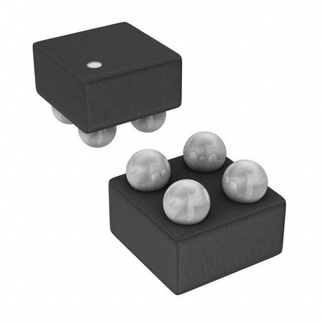
| 产品图片 |
|
| rohs | 符合RoHS无铅 / 符合限制有害物质指令(RoHS)规范要求 |
| 产品系列 | 电源管理 IC,线性稳压器,Texas Instruments UA78M08CDCYR- |
| 数据手册 | |
| 产品型号 | UA78M08CDCYR |
| PSRR/纹波抑制—典型值 | 80 dB |
| 产品目录页面 | |
| 产品种类 | |
| 供应商器件封装 | SOT-223 |
| 其它名称 | 296-12612-6 |
| 包装 | Digi-Reel® |
| 商标 | Texas Instruments |
| 安装类型 | 表面贴装 |
| 安装风格 | SMD/SMT |
| 封装 | Reel |
| 封装/外壳 | TO-261-4,TO-261AA |
| 封装/箱体 | SOT-223-4 |
| 工作温度 | 0°C ~ 125°C |
| 工厂包装数量 | 2500 |
| 最大工作温度 | + 125 C |
| 最大输入电压 | 25 V |
| 最小工作温度 | 0 C |
| 最小输入电压 | 10.5 V |
| 极性 | Positive |
| 标准包装 | 1 |
| 电压-跌落(典型值) | 2V @ 350mA |
| 电压-输入 | 10.5 V ~ 25 V |
| 电压-输出 | 8V |
| 电流-输出 | 500mA |
| 电流-限制(最小值) | - |
| 稳压器拓扑 | 正,固定式 |
| 稳压器数 | 1 |
| 系列 | UA78M08 |
| 线路调整率 | 100 mV |
| 负载调节 | 160 mV |
| 输出电压 | 8.3 V |
| 输出电流 | 0.5 A |
| 输出端数量 | 1 |
| 输出类型 | Fixed |


- 商务部:美国ITC正式对集成电路等产品启动337调查
- 曝三星4nm工艺存在良率问题 高通将骁龙8 Gen1或转产台积电
- 太阳诱电将投资9.5亿元在常州建新厂生产MLCC 预计2023年完工
- 英特尔发布欧洲新工厂建设计划 深化IDM 2.0 战略
- 台积电先进制程称霸业界 有大客户加持明年业绩稳了
- 达到5530亿美元!SIA预计今年全球半导体销售额将创下新高
- 英特尔拟将自动驾驶子公司Mobileye上市 估值或超500亿美元
- 三星加码芯片和SET,合并消费电子和移动部门,撤换高东真等 CEO
- 三星电子宣布重大人事变动 还合并消费电子和移动部门
- 海关总署:前11个月进口集成电路产品价值2.52万亿元 增长14.8%


PDF Datasheet 数据手册内容提取
Product Sample & Technical Tools & Support & Folder Buy Documents Software Community uA78M05,uA78M06,uA78M08 uA78M09,uA78M10,uA78M12,uA78M33 SLVS059T–JUNE1976–REVISEDJANUARY2015 µA78Mxx Positive-Voltage Regulators 1 Features 3 Description • 3-TerminalRegulators This series of fixed-voltage integrated-circuit voltage 1 regulators is designed for a wide range of • OutputCurrentupto500mA applications. The applications include on-card • NoExternalComponents regulation for elimination of noise and distribution • InternalThermal-OverloadProtection problems associated with single-point regulation. Each of these regulators can deliver up to 500 mA of • HighPower-DissipationCapability output current. The internal current-limiting and • InternalShort-CircuitCurrentLimiting thermal-shutdown features of these regulators • OutputTransistorSafe-AreaCompensation essentially make them immune to overload. In addition to use as fixed-voltage regulators, these 2 Applications devices can be used with external components to obtain adjustable output voltages and currents and • On-CardRegulation also as the power-pass element in precision • PortableDevices regulators. • Computing& Servers DeviceInformation(1) • Telecommunications PARTNUMBER PACKAGE BODYSIZE(NOM) SOT-223(3) 6.50mmx3.50mm UA78Mxx TO-220(3) 10.16mmx8.82mm TO-252(3) 6.60mmx6.10mm (1) For all available packages, see the orderable addendum at theendofthedatasheet. 4 Simplified Schematic Unregulated Voltage Source INPUT OUTPUT Up to 500 mA UA78MXX 0.33 PF COMMON 0.1 PF 1 An IMPORTANT NOTICE at the end of this data sheet addresses availability, warranty, changes, use in safety-critical applications, intellectualpropertymattersandotherimportantdisclaimers.PRODUCTIONDATA.
uA78M05,uA78M06,uA78M08 uA78M09,uA78M10,uA78M12,uA78M33 SLVS059T–JUNE1976–REVISEDJANUARY2015 www.ti.com Table of Contents 1 Features.................................................................. 1 7.14 TypicalCharacteristics............................................9 2 Applications........................................................... 1 8 DetailedDescription............................................ 10 3 Description............................................................. 1 8.1 Overview.................................................................10 4 SimplifiedSchematic............................................. 1 8.2 FunctionalBlockDiagram.......................................10 8.3 FeatureDescription.................................................10 5 RevisionHistory..................................................... 2 8.4 DeviceFunctionalModes........................................10 6 PinConfigurationandFunctions......................... 3 9 ApplicationandImplementation........................ 11 7 Specifications......................................................... 4 9.1 ApplicationInformation............................................11 7.1 AbsoluteMaximumRatings......................................4 9.2 TypicalApplication .................................................11 7.2 ESDRatings ............................................................4 10 PowerSupplyRecommendations..................... 13 7.3 RecommendedOperatingConditions.......................4 11 Layout................................................................... 13 7.4 ThermalInformation..................................................4 7.5 ElectricalCharacteristics—uA78M33C...................5 11.1 LayoutGuidelines.................................................13 7.6 ElectricalCharacteristics—uA78M33I.....................5 11.2 LayoutExample....................................................13 7.7 ElectricalCharacteristics—uA78M05C...................6 12 DeviceandDocumentationSupport................. 14 7.8 ElectricalCharacteristics—uA78M05I.....................6 12.1 RelatedLinks........................................................14 7.9 ElectricalCharacteristics—uA78M06C...................7 12.2 Trademarks...........................................................14 7.10 ElectricalCharacteristics—uA78M08C.................7 12.3 ElectrostaticDischargeCaution............................14 7.11 ElectricalCharacteristics—uA78M09C.................8 12.4 Glossary................................................................14 7.12 ElectricalCharacteristics—uA78M10C.................8 13 Mechanical,Packaging,andOrderable 7.13 ElectricalCharacteristics—uA78M12C.................9 Information........................................................... 14 5 Revision History ChangesfromRevisionS(May2013)toRevisionT Page • AddedApplications,DeviceInformationtable,PinFunctionstable,ESDRatingstable,ThermalInformationtable, TypicalCharacteristics,FeatureDescriptionsection,DeviceFunctionalModes,ApplicationandImplementation section,PowerSupplyRecommendationssection,Layoutsection,DeviceandDocumentationSupportsection,and Mechanical,Packaging,andOrderableInformationsection.................................................................................................. 1 ChangesfromRevisionR(February2013)toRevisionS Page • RemovedOrderingInformationtable..................................................................................................................................... 1 ChangesfromRevisionQ(April2010)toRevisionR Page • Removedobsoletepartinformationfromdocument.............................................................................................................. 1 2 SubmitDocumentationFeedback Copyright©1976–2015,TexasInstrumentsIncorporated ProductFolderLinks:uA78M05 uA78M06 uA78M08uA78M09 uA78M10 uA78M12 uA78M33
uA78M05,uA78M06,uA78M08 uA78M09,uA78M10,uA78M12,uA78M33 www.ti.com SLVS059T–JUNE1976–REVISEDJANUARY2015 6 Pin Configuration and Functions KC (TO-220) PACKAGE (TOPVIEW) KTP (PowerFLEX /TO-252*) PACKAGE N O OUTPUT (TOPVIEW) M COMMON OM INPUT ON OUTPUT C M COMMON M O INPUT C KCS (TO-220) PACKAGE (TOPVIEW) * Complies with JEDECTO-252, variation AC N O OUTPUT M M COMMON DCY (SOT-223) PACKAGE O INPUT (TOPVIEW) C OUTPUT N KVU (TO-252) PACKAGE O (TOPVIEW) M M COMMON N OUTPUT O O C M COMMON INPUT M O C INPUT PinFunctions PIN TYPE DESCRIPTION NAME NO. COMMON 2 — Ground INPUT 1 I SupplyInput OUTPUT 3 O VoltageOutput Copyright©1976–2015,TexasInstrumentsIncorporated SubmitDocumentationFeedback 3 ProductFolderLinks:uA78M05 uA78M06 uA78M08uA78M09 uA78M10 uA78M12 uA78M33
uA78M05,uA78M06,uA78M08 uA78M09,uA78M10,uA78M12,uA78M33 SLVS059T–JUNE1976–REVISEDJANUARY2015 www.ti.com 7 Specifications 7.1 Absolute Maximum Ratings overvirtualjunctiontemperaturerange(unlessotherwisenoted) (1) MIN MAX UNIT V Inputvoltage 35 V I T Operatingvirtualjunctiontemperature 150 °C J T Storagetemperaturerange –65 150 °C stg (1) StressesbeyondthoselistedunderAbsoluteMaximumRatingsmaycausepermanentdamagetothedevice.Thesearestressratings only,andfunctionaloperationofthedeviceattheseoranyotherconditionsbeyondthoseindicatedunderRecommendedOperating Conditionsisnotimplied.Exposuretoabsolute-maximum-ratedconditionsforextendedperiodsmayaffectdevicereliability. 7.2 ESD Ratings VALUE UNIT Humanbodymodel(HBM),perANSI/ESDA/JEDECJS-001,allpins(1) 2500 V(ESD) Electrostaticdischarge Chargeddevicemodel(CDM),perJEDECspecificationJESD22-C101, V allpins(2) 2000 (1) JEDECdocumentJEP155statesthat500-VHBMallowssafemanufacturingwithastandardESDcontrolprocess. (2) JEDECdocumentJEP157statesthat250-VCDMallowssafemanufacturingwithastandardESDcontrolprocess. 7.3 Recommended Operating Conditions MIN MAX UNIT uA78M33 5.3 25 uA78M05 7 25 uA78M06 8 25 uA78M08 10.5 25 V Inputvoltage V I uA78M09 11.5 26 uA78M10 12.5 28 uA78M12 14.5 30 uA78M15 17.5 30 I Outputcurrent 500 mA O uA78MxxC 0 125 T Operatingvirtualjunctiontemperature °C J uA78MxxI –40 125 7.4 Thermal Information UA78Mxx THERMALMETRIC(1) DCY KC KCS KTP KVU UNIT 3PINS 3PINS 3PINS 3PINS 3PINS R Junction-to-ambientthermalresistance 53 19 19 28 30.3 θJA R θJC(to Junction-to-case(top)thermalresistance 30.6 17 17 19 — °C/W p) R θJC(b Junction-to-case(bottom)thermalresistance — 3 3 1.4 — ot) (1) Formoreinformationabouttraditionalandnewthermalmetrics,seetheICPackageThermalMetricsapplicationreport,SPRA953. 4 SubmitDocumentationFeedback Copyright©1976–2015,TexasInstrumentsIncorporated ProductFolderLinks:uA78M05 uA78M06 uA78M08uA78M09 uA78M10 uA78M12 uA78M33
uA78M05,uA78M06,uA78M08 uA78M09,uA78M10,uA78M12,uA78M33 www.ti.com SLVS059T–JUNE1976–REVISEDJANUARY2015 7.5 Electrical Characteristics — uA78M33C atspecifiedvirtualjunctiontemperature,V =8V,I =350mA,T =25°C(unlessotherwisenoted) I O J uA78M33C PARAMETER0 TESTCONDITIONS(1) UNIT MIN TYP MAX Outputvoltage(2) IO=5mAto350mA, 3.2 3.3 3.4 V VI=8Vto20V TJ=0°Cto125°C 3.1 3.3 3.5 V =5.3Vto25V 9 100 I Inputvoltageregulation I =200mA mV O V =8Vto25V 3 50 I Ripplerejection VI=8Vto18V, IO=100mA,TJ=0°Cto125°C 62 dB f=120Hz I =300mA 62 80 O Outputvoltageregulation V =8V, I =5mAto500mA 20 100 mV I O Temperaturecoefficient I =5mA, T =0°Cto125°C –1 mV/°C ofoutputvoltage O J Outputnoisevoltage f=10Hzto100kHz 40 200 μV Dropoutvoltage 2 V Biascurrent 4.5 6 mA I =200mA, V =8Vto25V, T =0°Cto125°C 0.8 O I J Biascurrentchange mA I =5mAto350mA, T =0°Cto125°C 0.5 O J Short-circuitoutput V =35V 300 mA current I Peakoutputcurrent 700 mA (1) Allcharacteristicsaremeasuredwitha0.33-μFcapacitoracrosstheinputanda0.1-μFcapacitoracrosstheoutput.Pulse-testing techniquesmaintainT asclosetoT aspossible.Thermaleffectsmustbetakenintoaccountseparately. J A (2) ThisspecificationappliesonlyfordcpowerdissipationpermittedbyAbsoluteMaximumRatings. 7.6 Electrical Characteristics — uA78M33I atspecifiedvirtualjunctiontemperature,V =8V,I =350mA,T =25°C(unlessotherwisenoted) I O J uA78M33I PARAMETER TESTCONDITIONS(1) UNIT MIN TYP MAX Outputvoltage(2) IO=5mAto350mA, 3.2 3.3 3.4 V VI=8Vto20V TJ=–40°Cto125°C 3.1 3.3 3.5 V =5.3Vto25V 9 100 I Inputvoltageregulation I =200mA mV O V =8Vto25V 3 50 I I =100mA,T =–40°Cto Ripplerejection VI=8Vto18V, 1O25°C J 62 dB f=120Hz I =300mA 62 80 O Outputvoltageregulation V =8V, I =5mAto500mA 20 100 mV I O Temperaturecoefficient I =5mA, T =–40°Cto125°C –1 mV/°C ofoutputvoltage O J Outputnoisevoltage f=10Hzto100kHz 40 200 μV Dropoutvoltage 2 V Biascurrent 4.5 6 mA I =200mA, V =8Vto25V, T =–40°Cto125°C 0.8 O I J Biascurrentchange mA I =5mAto350mA, T =–40°Cto125°C 0.5 O J Short-circuitoutput V =35V 300 mA current I Peakoutputcurrent 700 mA (1) Allcharacteristicsaremeasuredwitha0.33-μFcapacitoracrosstheinputanda0.1-μFcapacitoracrosstheoutput.Pulse-testing techniquesmaintainT asclosetoT aspossible.Thermaleffectsmustbetakenintoaccountseparately. J A (2) ThisspecificationappliesonlyfordcpowerdissipationpermittedbyAbsoluteMaximumRatings. Copyright©1976–2015,TexasInstrumentsIncorporated SubmitDocumentationFeedback 5 ProductFolderLinks:uA78M05 uA78M06 uA78M08uA78M09 uA78M10 uA78M12 uA78M33
uA78M05,uA78M06,uA78M08 uA78M09,uA78M10,uA78M12,uA78M33 SLVS059T–JUNE1976–REVISEDJANUARY2015 www.ti.com 7.7 Electrical Characteristics — uA78M05C atspecifiedvirtualjunctiontemperature,V =10V,I =350mA,T =25°C(unlessotherwisenoted) I O J uA78M05C PARAMETER TESTCONDITIONS(1) UNIT MIN TYP MAX Outputvoltage(2) IO=5mAto350mA, 4.8 5 5.2 V VI=7Vto20V TJ=0°Cto125°C 4.75 5.25 V =7Vto25V 3 100 I Inputvoltageregulation I =200mA mV O V =8Vto25V 1 50 I Ripplerejection VI=8Vto18V, IO=100mA,TJ=0°Cto125°C 62 dB f=120Hz I =300mA 62 80 O I =5mAto500mA 20 100 O Outputvoltageregulation mV I =5mAto200mA 10 50 O Temperaturecoefficient I =5mA, T =0°Cto125°C –1 mV/°C ofoutputvoltage O J Outputnoisevoltage f=10Hzto100kHz 40 200 μV Dropoutvoltage 2 V Biascurrent 4.5 6 mA I =200mA,V =8Vto25V,T =0°Cto125°C 0.8 O I J Biascurrentchange mA I =5mAto350mA, T =0°Cto125°C 0.5 O J Short-circuitoutputcurrent V =35V 300 mA I Peakoutputcurrent 0.7 A (1) Allcharacteristicsaremeasuredwitha0.33-μFcapacitoracrosstheinputanda0.1-μFcapacitoracrosstheoutput.Pulse-testing techniquesmaintainT asclosetoT aspossible.Thermaleffectsmustbetakenintoaccountseparately. J A (2) ThisspecificationappliesonlyfordcpowerdissipationpermittedbyAbsoluteMaximumRatings. 7.8 Electrical Characteristics — uA78M05I atspecifiedvirtualjunctiontemperature,V =10V,I =350mA,T =25°C(unlessotherwisenoted) I O J uA78M05I PARAMETER TESTCONDITIONS(1) UNIT MIN TYP MAX Outputvoltage(2) IO=5mAto350mA, 4.8 5 5.2 V VI=7Vto20V TJ=–40°Cto125°C 4.75 5.25 V =7Vto25V 3 100 I Inputvoltageregulation I =200mA mV O V =8Vto25V 1 50 I Ripplerejection VI=8Vto18V, IO=100mA,TJ=–40°Cto125°C 62 dB f=120Hz I =300mA 62 80 O Outputvoltage IO=5mAto500mA 20 100 mV regulation I =5mAto200mA 10 50 O Temperaturecoefficient I =5mA, T =–40°Cto125°C –1 mV/°C ofoutputvoltage O J Outputnoisevoltage f=10Hzto100kHz 40 200 μV Dropoutvoltage 2 V Biascurrent 4.5 6 mA I =200mA, V =8Vto25V, T =–40°Cto125°C 0.8 O I J Biascurrentchange mA I =5mAto350mA, T =–40°Cto125°C 0.5 O J Short-circuitoutput V =35V 300 mA current I Peakoutputcurrent 0.7 A (1) Allcharacteristicsaremeasuredwitha0.33-μFcapacitoracrosstheinputanda0.1-μFcapacitoracrosstheoutput.Pulse-testing techniquesmaintainT asclosetoT aspossible.Thermaleffectsmustbetakenintoaccountseparately. J A (2) ThisspecificationappliesonlyfordcpowerdissipationpermittedbyAbsoluteMaximumRatings. 6 SubmitDocumentationFeedback Copyright©1976–2015,TexasInstrumentsIncorporated ProductFolderLinks:uA78M05 uA78M06 uA78M08uA78M09 uA78M10 uA78M12 uA78M33
uA78M05,uA78M06,uA78M08 uA78M09,uA78M10,uA78M12,uA78M33 www.ti.com SLVS059T–JUNE1976–REVISEDJANUARY2015 7.9 Electrical Characteristics — uA78M06C atspecifiedvirtualjunctiontemperature,V =11V,I =350mA,T =25°C(unlessotherwisenoted) I O J uA78M06C PARAMETER TESTCONDITIONS(1) UNIT MIN TYP MAX 5.75 6 6.25 Outputvoltage(2) I =5mAto350mA, V =8Vto21V V O I T =0°Cto125°C 5.7 6.3 J V =8Vto25V 5 100 I Inputvoltageregulation I =200mA mV O V =9Vto25V 1.5 50 I I =100mA, O 59 Ripplerejection VI=8Vto18V, f=120Hz TJ=0°Cto125°C dB I =300mA 59 80 O I =5mAto500mA 20 120 O Outputvoltageregulation mV I =5mAto200mA 10 60 O Temperaturecoefficient I =5mA, T =0°Cto125°C –1 mV/°C ofoutputvoltage O J Outputnoisevoltage f=10Hzto100kHz 45 μV Dropoutvoltage 2 V Biascurrent 4.5 6 mA V =9Vto25V, I =200mA, T =0°Cto125°C 0.8 I O J Biascurrentchange mA I =5mAto350mA, T =0°Cto125°C 0.5 O J Short-circuitoutputcurrent V =35V 270 mA I Peakoutputcurrent 0.7 A (1) Allcharacteristicsaremeasuredwitha0.33-μFcapacitoracrosstheinputanda0.1-μFcapacitoracrosstheoutput.Pulse-testing techniquesmaintainT asclosetoT aspossible.Thermaleffectsmustbetakenintoaccountseparately. J A (2) ThisspecificationappliesonlyfordcpowerdissipationpermittedbyAbsoluteMaximumRatings. 7.10 Electrical Characteristics — uA78M08C atspecifiedvirtualjunctiontemperature,V =14V,I =350mA,T =25°C(unlessotherwisenoted) I O J uA78M08C PARAMETER TESTCONDITIONS(1) UNIT MIN TYP MAX 7.7 8 8.3 Outputvoltage(2) V =10.5Vto23V, I =5mAto350mA V I O T =0°Cto125°C 7.6 8.4 J V =10.5Vto25V 6 100 I Inputvoltageregulation I =200mA mV O V =11Vto25V 2 50 I Ripplerejection VI=11Vto21.5V, IO=100mA, TJ=0°Cto125°C 56 dB f=120Hz I =300mA 56 80 O I =5mAto500mA 25 160 O Outputvoltageregulation mV I =5mAto200mA 10 80 O Temperaturecoefficient I =5mA, T =0°Cto125°C –1 mV/°C ofoutputvoltage O J Outputnoisevoltage f=10Hzto100kHz 52 μV Dropoutvoltage 2 V Biascurrent 4.6 6 mA V =10.5Vto25V, I =200mA, T =0°Cto125°C 0.8 I O J Biascurrentchange mA I =5mAto350mA, T =0°Cto125°C 0.5 O J Short-circuitoutput V =35V 250 mA current I Peakoutputcurrent 0.7 A (1) Allcharacteristicsaremeasuredwitha0.33-μFcapacitoracrosstheinputanda0.1-μFcapacitoracrosstheoutput.Pulse-testing techniquesmaintainT asclosetoT aspossible.Thermaleffectsmustbetakenintoaccountseparately. J A (2) ThisspecificationappliesonlyfordcpowerdissipationpermittedbyAbsoluteMaximumRatings. Copyright©1976–2015,TexasInstrumentsIncorporated SubmitDocumentationFeedback 7 ProductFolderLinks:uA78M05 uA78M06 uA78M08uA78M09 uA78M10 uA78M12 uA78M33
uA78M05,uA78M06,uA78M08 uA78M09,uA78M10,uA78M12,uA78M33 SLVS059T–JUNE1976–REVISEDJANUARY2015 www.ti.com 7.11 Electrical Characteristics — uA78M09C atspecifiedvirtualjunctiontemperature,V =16V,I =350mA,T =25°C(unlessotherwisenoted) I O J uA78M09C PARAMETER TESTCONDITIONS(1) UNIT MIN TYP MAX 8.6 9 9.4 Outputvoltage(2) V =11.5Vto24V, I =5mAto350mA V I O T =0°Cto125°C 8.5 9.5 J V =11.5Vto26V 6 100 I Inputvoltageregulation I =200mA mV O V =12Vto26V 2 50 I Ripplerejection VI=13Vto23V, IO=100mA, TJ=0°Cto125°C 56 dB f=120Hz I =300mA 56 80 O I =5mAto500mA 25 180 O Outputvoltageregulation mV I =5mAto200mA 10 90 O Temperaturecoefficient I =5mA, T =0°Cto125°C –1 mV/°C ofoutputvoltage O J Outputnoisevoltage f=10Hzto100kHz 58 μV Dropoutvoltage 2 V Biascurrent 4.6 6 mA V =11.5Vto26V, I =200mA, T =0°Cto125°C 0.8 I O J Biascurrentchange mA I =5mAto350mA, T =0°Cto125°C 0.5 O J Short-circuitoutput V =35V 250 mA current I Peakoutputcurrent 0.7 A (1) Allcharacteristicsaremeasuredwitha0.33-μFcapacitoracrosstheinputanda0.1-μFcapacitoracrosstheoutput.Pulse-testing techniquesmaintainT asclosetoT aspossible.Thermaleffectsmustbetakenintoaccountseparately. J A (2) ThisspecificationappliesonlyfordcpowerdissipationpermittedbyAbsoluteMaximumRatings. 7.12 Electrical Characteristics — uA78M10C atspecifiedvirtualjunctiontemperature,V =17V,I =350mA,T =25°C(unlessotherwisenoted) I O J uA78M10C PARAMETER TESTCONDITIONS(1) UNIT MIN TYP MAX 9.6 10 10.4 Outputvoltage(2) V =12.5Vto25V, I =5mAto350mA V I O T =0°Cto125°C 9.5 10.5 J V =12.5Vto28V 7 100 I Inputvoltageregulation I =200mA mV O V =14Vto28V 2 50 I Ripplerejection VI=15Vto25V, IO=100mA, TJ=0°Cto125°C 59 dB f=120Hz I =300mA 55 80 O I =5mAto500mA 25 200 O Outputvoltageregulation mV I =5mAto200mA 10 100 O Temperaturecoefficient I =5mA, T =0°Cto125°C –1 mV/°C ofoutputvoltage O J Outputnoisevoltage f=10Hzto100kHz 64 μV Dropoutvoltage 2 V Biascurrent 4.7 6 mA V =12.5Vto28V, I =200mA, T =0°Cto125°C 0.8 I O J Biascurrentchange mA I =5mAto350mA, T =0°Cto125°C 0.5 O J Short-circuitoutput V =35V 245 mA current I Peakoutputcurrent 0.7 A (1) Allcharacteristicsaremeasuredwitha0.33-μFcapacitoracrosstheinputanda0.1-μFcapacitoracrosstheoutput.Pulse-testing techniquesmaintainT asclosetoT aspossible.Thermaleffectsmustbetakenintoaccountseparately. J A (2) ThisspecificationappliesonlyfordcpowerdissipationpermittedbyAbsoluteMaximumRatings. 8 SubmitDocumentationFeedback Copyright©1976–2015,TexasInstrumentsIncorporated ProductFolderLinks:uA78M05 uA78M06 uA78M08uA78M09 uA78M10 uA78M12 uA78M33
uA78M05,uA78M06,uA78M08 uA78M09,uA78M10,uA78M12,uA78M33 www.ti.com SLVS059T–JUNE1976–REVISEDJANUARY2015 7.13 Electrical Characteristics — uA78M12C atspecifiedvirtualjunctiontemperature,V =19V,I =350mA,T =25°C(unlessotherwisenoted) I O J uA78M12C PARAMETER TESTCONDITIONS(1) UNIT MIN TYP MAX 11.5 12 12.5 Outputvoltage(2) V =14.5Vto27V, I =5mAto350mA V I O T =0°Cto125°C 11.4 12.6 J V =14.5Vto30V 8 100 I Inputvoltageregulation I =200mA mV O V =16Vto30V 2 50 I Ripplerejection VI=15Vto25V, IO=100mA, TJ=0°Cto125°C 55 dB f=120Hz I =300mA 55 80 O I =5mAto500mA 25 240 O Outputvoltageregulation mV I =5mAto200mA 10 120 O Temperaturecoefficient I =5mA, T =0°Cto125°C –1 mV/°C ofoutputvoltage O J Outputnoisevoltage f=10Hzto100kHz 75 μV Dropoutvoltage 2 V Biascurrent 4.8 6 mA V =14.5Vto30V, I =200mA, T =0°Cto125°C 0.8 I O J Biascurrentchange mA I =5mAto350mA, T =0°Cto125°C 0.5 O J Short-circuitoutput V =35V 240 mA current I Peakoutputcurrent 0.7 A (1) Allcharacteristicsaremeasuredwitha0.33-μFcapacitoracrosstheinputanda0.1-μFcapacitoracrosstheoutput.Pulse-testing techniquesmaintainT asclosetoT aspossible.Thermaleffectsmustbetakenintoaccountseparately. J A (2) ThisspecificationappliesonlyfordcpowerdissipationpermittedbyAbsoluteMaximumRatings. 7.14 Typical Characteristics 120 100 b) (d 80 n o cti e 60 ej R e pl 40 p Ri 20 Ioutat100mA Ioutat300mA 0 120Hz 240Hz 500Hz 1KHz Frequency C002 Figure1.RippleRejectionvsFrequency V_INPUT=8Vto18V,TA=25°C Copyright©1976–2015,TexasInstrumentsIncorporated SubmitDocumentationFeedback 9 ProductFolderLinks:uA78M05 uA78M06 uA78M08uA78M09 uA78M10 uA78M12 uA78M33
uA78M05,uA78M06,uA78M08 uA78M09,uA78M10,uA78M12,uA78M33 SLVS059T–JUNE1976–REVISEDJANUARY2015 www.ti.com 8 Detailed Description 8.1 Overview This series of fixed-voltage integrated-circuit voltage regulators is designed for a wide range of applications. The applications include on-card regulation for elimination of noise and distribution problems associated with single- point regulation. Each of these regulators can deliver up to 500 mA of output current. The internal current-limiting and thermal-shutdown features of these regulators essentially make them immune to overload. In addition to use as fixed-voltage regulators, these devices can be used with external components to obtain adjustable output voltagesandcurrentsandalsoasthepower-passelementinprecisionregulators. 8.2 Functional Block Diagram INPUT 140 kΩ 96Ω 0.6Ω OUTPUT 0 to 20 kΩ 5.4 kΩ COMMON Resistor values shown are nominal. 8.3 Feature Description • 3-TerminalRegulators • OutputCurrentupto500mA • NoExternalComponents • InternalThermal-OverloadProtection • HighPower-DissipationCapability • InternalShort-CircuitCurrentLimiting • OutputTransistorSafe-AreaCompensation 8.4 Device Functional Modes 8.4.1 Fixed-OutputMode Thesedevicesareavailableinfixed-outputvoltages.Seetheorderablepartlistforthedesiredoutput. 10 SubmitDocumentationFeedback Copyright©1976–2015,TexasInstrumentsIncorporated ProductFolderLinks:uA78M05 uA78M06 uA78M08uA78M09 uA78M10 uA78M12 uA78M33
uA78M05,uA78M06,uA78M08 uA78M09,uA78M10,uA78M12,uA78M33 www.ti.com SLVS059T–JUNE1976–REVISEDJANUARY2015 9 Application and Implementation NOTE Information in the following applications sections is not part of the TI component specification, and TI does not warrant its accuracy or completeness. TI’s customers are responsible for determining suitability of components for their purposes. Customers should validateandtesttheirdesignimplementationtoconfirmsystemfunctionality. 9.1 Application Information The UA78Mxx devices are ideal for use as linear regulators with few external components needed for a working design.Theyarealsousefulforattenuatingpowersupplynoise. 9.2 Typical Application Unregulated Voltage Source INPUT OUTPUT Up to 500 mA UA78MXX 0.33 PF COMMON 0.1 PF Figure2. Fixed-OutputRegulator 9.2.1 DesignRequirements An 0.33-µF decoupling capacitor on the input and a 0.1-µF decoupling capacitor on the output are recommended fortheUA78Mxxtobehaveasclosetodatasheetspecificationsaspossible. 9.2.2 DetailedDesignProcedure The customer's end application will determine how the schematic for UA78Mxx is designed. For example, if there is a load connected to a negative voltage as its ground, a clamp diode may be necessary on the output. In the event of an input short circuit or another case where the output voltage can be higher than the input, a diode shuntcanbeconnectedacrossthedevicewiththeanodeattheoutputandcathodeattheinput Copyright©1976–2015,TexasInstrumentsIncorporated SubmitDocumentationFeedback 11 ProductFolderLinks:uA78M05 uA78M06 uA78M08uA78M09 uA78M10 uA78M12 uA78M33
uA78M05,uA78M06,uA78M08 uA78M09,uA78M10,uA78M12,uA78M33 SLVS059T–JUNE1976–REVISEDJANUARY2015 www.ti.com Typical Application (continued) 9.2.3 ApplicationCurves 5.50 5.25 (V)5.00 e g a olt4.75 V ut p ut4.50 O 4.25 5mA 500mA 4.00 6.00 6.25 6.50 6.75 7.00 7.25 7.50 7.75 8.00 InputVoltage(V) C001 Figure3.V_OUTPUTvsV_INPUTfor I =5mAand500mA(25°C) OUTPUT 12 SubmitDocumentationFeedback Copyright©1976–2015,TexasInstrumentsIncorporated ProductFolderLinks:uA78M05 uA78M06 uA78M08uA78M09 uA78M10 uA78M12 uA78M33
uA78M05,uA78M06,uA78M08 uA78M09,uA78M10,uA78M12,uA78M33 www.ti.com SLVS059T–JUNE1976–REVISEDJANUARY2015 10 Power Supply Recommendations See Recommended Operating Conditions for the recommended power supply voltages for each variation of the UA78Mxx. Different orderable part numbers will be able to tolerate different levels of voltage. It is also recommendedtohaveadecouplingcapacitorontheoutputtolimitnoiseontheinput. 11 Layout 11.1 Layout Guidelines Keep trace widths large enough to eliminate problematic I×R voltage drops at the input and output terminals. InputdecouplingcapacitorsshouldbeplacedasclosetotheUA78MXXaspossible. 11.2 Layout Example COMMON IN C O P O U U M T T M P (cid:19)(cid:17)(cid:22)(cid:22)(cid:3)PF O U (cid:19)(cid:17)(cid:20)(cid:3)PF T N Ground Ground Figure4. LayoutDiagram Copyright©1976–2015,TexasInstrumentsIncorporated SubmitDocumentationFeedback 13 ProductFolderLinks:uA78M05 uA78M06 uA78M08uA78M09 uA78M10 uA78M12 uA78M33
uA78M05,uA78M06,uA78M08 uA78M09,uA78M10,uA78M12,uA78M33 SLVS059T–JUNE1976–REVISEDJANUARY2015 www.ti.com 12 Device and Documentation Support 12.1 Related Links The table below lists quick access links. Categories include technical documents, support and community resources,toolsandsoftware,andquickaccesstosampleorbuy. Table1.RelatedLinks TECHNICAL TOOLS& SUPPORT& PARTS PRODUCTFOLDER SAMPLE&BUY DOCUMENTS SOFTWARE COMMUNITY uA78M05 Clickhere Clickhere Clickhere Clickhere Clickhere uA78M06 Clickhere Clickhere Clickhere Clickhere Clickhere uA78M08 Clickhere Clickhere Clickhere Clickhere Clickhere uA78M09 Clickhere Clickhere Clickhere Clickhere Clickhere uA78M10 Clickhere Clickhere Clickhere Clickhere Clickhere uA78M12 Clickhere Clickhere Clickhere Clickhere Clickhere uA78M33 Clickhere Clickhere Clickhere Clickhere Clickhere 12.2 Trademarks Alltrademarksarethepropertyoftheirrespectiveowners. 12.3 Electrostatic Discharge Caution Thesedeviceshavelimitedbuilt-inESDprotection.Theleadsshouldbeshortedtogetherorthedeviceplacedinconductivefoam duringstorageorhandlingtopreventelectrostaticdamagetotheMOSgates. 12.4 Glossary SLYZ022—TIGlossary. Thisglossarylistsandexplainsterms,acronyms,anddefinitions. 13 Mechanical, Packaging, and Orderable Information The following pages include mechanical, packaging, and orderable information. This information is the most current data available for the designated devices. This data is subject to change without notice and revision of thisdocument.Forbrowser-basedversionsofthisdatasheet,refertotheleft-handnavigation. 14 SubmitDocumentationFeedback Copyright©1976–2015,TexasInstrumentsIncorporated ProductFolderLinks:uA78M05 uA78M06 uA78M08uA78M09 uA78M10 uA78M12 uA78M33
PACKAGE OPTION ADDENDUM www.ti.com 6-Feb-2020 PACKAGING INFORMATION Orderable Device Status Package Type Package Pins Package Eco Plan Lead/Ball Finish MSL Peak Temp Op Temp (°C) Device Marking Samples (1) Drawing Qty (2) (6) (3) (4/5) SN78MCDCYR ACTIVE SOT-223 DCY 4 2500 Green (RoHS SN Level-2-260C-1 YEAR 0 to 125 C5 & no Sb/Br) UA78M05CDCY ACTIVE SOT-223 DCY 4 80 Green (RoHS SN Level-2-260C-1 YEAR 0 to 125 C5 & no Sb/Br) UA78M05CDCYG3 ACTIVE SOT-223 DCY 4 80 Green (RoHS SN Level-2-260C-1 YEAR 0 to 125 C5 & no Sb/Br) UA78M05CDCYR ACTIVE SOT-223 DCY 4 2500 Green (RoHS SN Level-2-260C-1 YEAR 0 to 125 C5 & no Sb/Br) UA78M05CDCYRG3 ACTIVE SOT-223 DCY 4 2500 Green (RoHS SN Level-2-260C-1 YEAR 0 to 125 C5 & no Sb/Br) UA78M05CKCS ACTIVE TO-220 KCS 3 50 Pb-Free SN N / A for Pkg Type 0 to 125 UA78M05C (RoHS) UA78M05CKCSE3 ACTIVE TO-220 KCS 3 50 Pb-Free SN N / A for Pkg Type 0 to 125 UA78M05C (RoHS) UA78M05CKVURG3 ACTIVE TO-252 KVU 3 2500 Green (RoHS SN Level-3-260C-168 HR 0 to 125 78M05C & no Sb/Br) UA78M05IDCY ACTIVE SOT-223 DCY 4 80 Green (RoHS SN Level-2-260C-1 YEAR -40 to 125 J5 & no Sb/Br) UA78M05IDCYG3 ACTIVE SOT-223 DCY 4 80 Green (RoHS SN Level-2-260C-1 YEAR -40 to 125 J5 & no Sb/Br) UA78M05IDCYR ACTIVE SOT-223 DCY 4 2500 Green (RoHS SN Level-2-260C-1 YEAR -40 to 125 J5 & no Sb/Br) UA78M05IDCYRG3 ACTIVE SOT-223 DCY 4 2500 Green (RoHS SN Level-2-260C-1 YEAR -40 to 125 J5 & no Sb/Br) UA78M05IKCS ACTIVE TO-220 KCS 3 50 Pb-Free SN N / A for Pkg Type -40 to 125 UA78M05I (RoHS) UA78M05IKCSE3 ACTIVE TO-220 KCS 3 50 Pb-Free SN N / A for Pkg Type -40 to 125 UA78M05I (RoHS) UA78M05IKVURG3 ACTIVE TO-252 KVU 3 2500 Green (RoHS SN Level-3-260C-168 HR -40 to 125 78M05I & no Sb/Br) UA78M06CKVURG3 ACTIVE TO-252 KVU 3 2500 Green (RoHS SN Level-3-260C-168 HR 0 to 125 78M06C & no Sb/Br) UA78M08CDCY ACTIVE SOT-223 DCY 4 80 Green (RoHS SN Level-2-260C-1 YEAR 0 to 125 C8 & no Sb/Br) Addendum-Page 1
PACKAGE OPTION ADDENDUM www.ti.com 6-Feb-2020 Orderable Device Status Package Type Package Pins Package Eco Plan Lead/Ball Finish MSL Peak Temp Op Temp (°C) Device Marking Samples (1) Drawing Qty (2) (6) (3) (4/5) UA78M08CDCYG3 ACTIVE SOT-223 DCY 4 80 Green (RoHS SN Level-2-260C-1 YEAR 0 to 125 C8 & no Sb/Br) UA78M08CDCYR ACTIVE SOT-223 DCY 4 2500 Green (RoHS SN Level-2-260C-1 YEAR 0 to 125 C8 & no Sb/Br) UA78M08CKCS ACTIVE TO-220 KCS 3 50 Pb-Free SN N / A for Pkg Type 0 to 125 UA78M08C (RoHS) UA78M08CKCSE3 ACTIVE TO-220 KCS 3 50 Pb-Free SN N / A for Pkg Type 0 to 125 UA78M08C (RoHS) UA78M08CKVURG3 ACTIVE TO-252 KVU 3 2500 Green (RoHS SN Level-3-260C-168 HR 0 to 125 78M08C & no Sb/Br) UA78M09CKVURG3 ACTIVE TO-252 KVU 3 2500 Green (RoHS SN Level-3-260C-168 HR 0 to 125 78M09C & no Sb/Br) UA78M10CKVURG3 ACTIVE TO-252 KVU 3 2500 Green (RoHS SN Level-3-260C-168 HR 0 to 125 78M10C & no Sb/Br) UA78M12CKCS ACTIVE TO-220 KCS 3 50 Pb-Free SN N / A for Pkg Type 0 to 125 UA78M12C (RoHS) UA78M12CKCSE3 ACTIVE TO-220 KCS 3 50 Pb-Free SN N / A for Pkg Type 0 to 125 UA78M12C (RoHS) UA78M12CKVURG3 ACTIVE TO-252 KVU 3 2500 Green (RoHS SN Level-3-260C-168 HR 0 to 125 78M12C & no Sb/Br) UA78M33CDCY ACTIVE SOT-223 DCY 4 80 Green (RoHS SN Level-2-260C-1 YEAR 0 to 125 C3 & no Sb/Br) UA78M33CDCYG3 ACTIVE SOT-223 DCY 4 80 Green (RoHS SN Level-2-260C-1 YEAR 0 to 125 C3 & no Sb/Br) UA78M33CDCYR ACTIVE SOT-223 DCY 4 2500 Green (RoHS SN Level-2-260C-1 YEAR 0 to 125 C3 & no Sb/Br) UA78M33CDCYRG3 ACTIVE SOT-223 DCY 4 2500 Green (RoHS SN Level-2-260C-1 YEAR 0 to 125 C3 & no Sb/Br) UA78M33CKCS ACTIVE TO-220 KCS 3 50 Pb-Free SN N / A for Pkg Type 0 to 125 UA78M33C (RoHS) UA78M33CKCSE3 ACTIVE TO-220 KCS 3 50 Pb-Free SN N / A for Pkg Type 0 to 125 UA78M33C (RoHS) UA78M33CKVURG3 ACTIVE TO-252 KVU 3 2500 Green (RoHS SN Level-3-260C-168 HR 0 to 125 78M33C & no Sb/Br) UA78M33IKVURG3 ACTIVE TO-252 KVU 3 2500 Green (RoHS SN Level-3-260C-168 HR -40 to 125 78M33I & no Sb/Br) Addendum-Page 2
PACKAGE OPTION ADDENDUM www.ti.com 6-Feb-2020 (1) The marketing status values are defined as follows: ACTIVE: Product device recommended for new designs. LIFEBUY: TI has announced that the device will be discontinued, and a lifetime-buy period is in effect. NRND: Not recommended for new designs. Device is in production to support existing customers, but TI does not recommend using this part in a new design. PREVIEW: Device has been announced but is not in production. Samples may or may not be available. OBSOLETE: TI has discontinued the production of the device. (2) RoHS: TI defines "RoHS" to mean semiconductor products that are compliant with the current EU RoHS requirements for all 10 RoHS substances, including the requirement that RoHS substance do not exceed 0.1% by weight in homogeneous materials. Where designed to be soldered at high temperatures, "RoHS" products are suitable for use in specified lead-free processes. TI may reference these types of products as "Pb-Free". RoHS Exempt: TI defines "RoHS Exempt" to mean products that contain lead but are compliant with EU RoHS pursuant to a specific EU RoHS exemption. Green: TI defines "Green" to mean the content of Chlorine (Cl) and Bromine (Br) based flame retardants meet JS709B low halogen requirements of <=1000ppm threshold. Antimony trioxide based flame retardants must also meet the <=1000ppm threshold requirement. (3) MSL, Peak Temp. - The Moisture Sensitivity Level rating according to the JEDEC industry standard classifications, and peak solder temperature. (4) There may be additional marking, which relates to the logo, the lot trace code information, or the environmental category on the device. (5) Multiple Device Markings will be inside parentheses. Only one Device Marking contained in parentheses and separated by a "~" will appear on a device. If a line is indented then it is a continuation of the previous line and the two combined represent the entire Device Marking for that device. (6) Lead/Ball Finish - Orderable Devices may have multiple material finish options. Finish options are separated by a vertical ruled line. Lead/Ball Finish values may wrap to two lines if the finish value exceeds the maximum column width. Important Information and Disclaimer:The information provided on this page represents TI's knowledge and belief as of the date that it is provided. TI bases its knowledge and belief on information provided by third parties, and makes no representation or warranty as to the accuracy of such information. Efforts are underway to better integrate information from third parties. TI has taken and continues to take reasonable steps to provide representative and accurate information but may not have conducted destructive testing or chemical analysis on incoming materials and chemicals. TI and TI suppliers consider certain information to be proprietary, and thus CAS numbers and other limited information may not be available for release. In no event shall TI's liability arising out of such information exceed the total purchase price of the TI part(s) at issue in this document sold by TI to Customer on an annual basis. OTHER QUALIFIED VERSIONS OF UA78M : •Automotive: UA78M-Q1 NOTE: Qualified Version Definitions: •Automotive - Q100 devices qualified for high-reliability automotive applications targeting zero defects Addendum-Page 3
PACKAGE MATERIALS INFORMATION www.ti.com 3-Aug-2017 TAPE AND REEL INFORMATION *Alldimensionsarenominal Device Package Package Pins SPQ Reel Reel A0 B0 K0 P1 W Pin1 Type Drawing Diameter Width (mm) (mm) (mm) (mm) (mm) Quadrant (mm) W1(mm) UA78M05CDCYR SOT-223 DCY 4 2500 330.0 12.4 7.0 7.42 2.0 8.0 12.0 Q3 UA78M05CDCYR SOT-223 DCY 4 2500 330.0 12.4 6.55 7.25 1.9 8.0 12.0 Q3 UA78M05CKVURG3 TO-252 KVU 3 2500 330.0 16.4 6.9 10.5 2.7 8.0 16.0 Q2 UA78M05CKVURG3 TO-252 KVU 3 2500 330.0 16.4 6.9 10.5 2.8 8.0 16.0 Q2 UA78M05IDCYR SOT-223 DCY 4 2500 330.0 12.4 6.55 7.25 1.9 8.0 12.0 Q3 UA78M05IDCYR SOT-223 DCY 4 2500 330.0 12.4 7.0 7.42 2.0 8.0 12.0 Q3 UA78M05IDCYR SOT-223 DCY 4 2500 330.0 12.4 7.05 7.4 1.9 8.0 12.0 Q3 UA78M05IKVURG3 TO-252 KVU 3 2500 330.0 16.4 6.9 10.5 2.7 8.0 16.0 Q2 UA78M05IKVURG3 TO-252 KVU 3 2500 330.0 16.4 6.9 10.5 2.8 8.0 16.0 Q2 UA78M06CKVURG3 TO-252 KVU 3 2500 330.0 16.4 6.9 10.5 2.7 8.0 16.0 Q2 UA78M08CDCYR SOT-223 DCY 4 2500 330.0 12.4 7.0 7.42 2.0 8.0 12.0 Q3 UA78M08CDCYR SOT-223 DCY 4 2500 330.0 12.4 7.05 7.4 1.9 8.0 12.0 Q3 UA78M08CKVURG3 TO-252 KVU 3 2500 330.0 16.4 6.9 10.5 2.7 8.0 16.0 Q2 UA78M09CKVURG3 TO-252 KVU 3 2500 330.0 16.4 6.9 10.5 2.7 8.0 16.0 Q2 UA78M10CKVURG3 TO-252 KVU 3 2500 330.0 16.4 6.9 10.5 2.8 8.0 16.0 Q2 UA78M10CKVURG3 TO-252 KVU 3 2500 330.0 16.4 6.9 10.5 2.7 8.0 16.0 Q2 UA78M12CKVURG3 TO-252 KVU 3 2500 330.0 16.4 6.9 10.5 2.7 8.0 16.0 Q2 UA78M33CDCYR SOT-223 DCY 4 2500 330.0 12.4 7.05 7.4 1.9 8.0 12.0 Q3 PackMaterials-Page1
PACKAGE MATERIALS INFORMATION www.ti.com 3-Aug-2017 Device Package Package Pins SPQ Reel Reel A0 B0 K0 P1 W Pin1 Type Drawing Diameter Width (mm) (mm) (mm) (mm) (mm) Quadrant (mm) W1(mm) UA78M33CDCYR SOT-223 DCY 4 2500 330.0 12.4 7.0 7.42 2.0 8.0 12.0 Q3 UA78M33CDCYR SOT-223 DCY 4 2500 330.0 12.4 6.55 7.25 1.9 8.0 12.0 Q3 UA78M33CKVURG3 TO-252 KVU 3 2500 330.0 16.4 6.9 10.5 2.7 8.0 16.0 Q2 UA78M33IKVURG3 TO-252 KVU 3 2500 330.0 16.4 6.9 10.5 2.8 8.0 16.0 Q2 UA78M33IKVURG3 TO-252 KVU 3 2500 330.0 16.4 6.9 10.5 2.7 8.0 16.0 Q2 *Alldimensionsarenominal Device PackageType PackageDrawing Pins SPQ Length(mm) Width(mm) Height(mm) UA78M05CDCYR SOT-223 DCY 4 2500 350.0 334.0 47.0 UA78M05CDCYR SOT-223 DCY 4 2500 336.0 336.0 48.0 UA78M05CKVURG3 TO-252 KVU 3 2500 340.0 340.0 38.0 UA78M05CKVURG3 TO-252 KVU 3 2500 350.0 334.0 47.0 UA78M05IDCYR SOT-223 DCY 4 2500 336.0 336.0 48.0 UA78M05IDCYR SOT-223 DCY 4 2500 350.0 334.0 47.0 UA78M05IDCYR SOT-223 DCY 4 2500 340.0 340.0 38.0 UA78M05IKVURG3 TO-252 KVU 3 2500 340.0 340.0 38.0 UA78M05IKVURG3 TO-252 KVU 3 2500 350.0 334.0 47.0 UA78M06CKVURG3 TO-252 KVU 3 2500 340.0 340.0 38.0 UA78M08CDCYR SOT-223 DCY 4 2500 350.0 334.0 47.0 UA78M08CDCYR SOT-223 DCY 4 2500 340.0 340.0 38.0 PackMaterials-Page2
PACKAGE MATERIALS INFORMATION www.ti.com 3-Aug-2017 Device PackageType PackageDrawing Pins SPQ Length(mm) Width(mm) Height(mm) UA78M08CKVURG3 TO-252 KVU 3 2500 340.0 340.0 38.0 UA78M09CKVURG3 TO-252 KVU 3 2500 340.0 340.0 38.0 UA78M10CKVURG3 TO-252 KVU 3 2500 350.0 334.0 47.0 UA78M10CKVURG3 TO-252 KVU 3 2500 340.0 340.0 38.0 UA78M12CKVURG3 TO-252 KVU 3 2500 340.0 340.0 38.0 UA78M33CDCYR SOT-223 DCY 4 2500 340.0 340.0 38.0 UA78M33CDCYR SOT-223 DCY 4 2500 350.0 334.0 47.0 UA78M33CDCYR SOT-223 DCY 4 2500 336.0 336.0 48.0 UA78M33CKVURG3 TO-252 KVU 3 2500 340.0 340.0 38.0 UA78M33IKVURG3 TO-252 KVU 3 2500 350.0 334.0 47.0 UA78M33IKVURG3 TO-252 KVU 3 2500 340.0 340.0 38.0 PackMaterials-Page3
None
PACKAGE OUTLINE KVU0003A TO-252 - 2.52 mm max height SCALE 1.500 TO-252 10.41 9.40 6.22 1.27 B A 5.97 0.89 1 2.29 6.70 2 5.460 6.35 4.58 4.953 3 0.890 3X 1.02 0.635 OPTIONAL NOTE 3 0.61 0.25 C A B 0.61 2.52 MAX C 0.46 0.61 0.46 SEE DETAIL A 5.21 MIN 3 4.32 2 4 MIN 1 EXPOSED 0.51 THERMAL PAD GAGE PLANE NOTE 3 0.13 0 -8 1.78 0.00 1.40 DETA 7.000AIL A TYPICAL 4218915/A 02/2017 NOTES: 1. All linear dimensions are in millimeters. Any dimensions in parenthesis are for reference only. Dimensioning and tolerancing per ASME Y14.5M. 2. This drawing is subject to change without notice. 3. Shape may vary per different assembly sites. 4. Reference JEDEC registration TO-252. www.ti.com
EXAMPLE BOARD LAYOUT KVU0003A TO-252 - 2.52 mm max height TO-252 2X (2.75) (6.15) 2X (1) 1 4 SYMM (4.58) (5.55) 3 (R0.05) TYP (4.2) (2.5) PKG LAND PATTERN EXAMPLE EXPOSED METAL SHOWN SCALE:6X 0.07 MAX 0.07 MIN ALL AROUND ALL AROUND EXPOSED METAL EXPOSED METAL SOLDER MASK METAL METAL UNDER SOLDER MASK OPENING SOLDER MASK OPENING NON SOLDER MASK SOLDER MASK DEFINED DEFINED SOLDER MASK DETAILS NOT TO SCALE 4218915/A 02/2017 NOTES: (continued) 5. This package is designed to be soldered to a thermal pad on the board. For more information, see Texas Instruments literature numbers SLMA002(www.ti.com/lit/slm002) and SLMA004 (www.ti.com/lit/slma004). 6. Vias are optional depending on application, refer to device data sheet. It is recommended that vias under paste be filled, plugged or tented. www.ti.com
EXAMPLE STENCIL DESIGN KVU0003A TO-252 - 2.52 mm max height TO-252 (1.18) TYP 2X (2.75) 2X (1) (0.14) 1 (R0.05) (1.33) TYP SYMM (4.58) 4 3 20X (1.13) (4.2) 20X (0.98) PKG SOLDER PASTE EXAMPLE BASED ON 0.125 mm THICK STENCIL EXPOSED PAD 65% PRINTED SOLDER COVERAGE BY AREA SCALE:8X 4218915/A 02/2017 NOTES: (continued) 7. Laser cutting apertures with trapezoidal walls and rounded corners may offer better paste release. IPC-7525 may have alternate design recommendations. 8. Board assembly site may have different recommendations for stencil design. www.ti.com
MECHANICAL DATA MPDS094A – APRIL 2001 – REVISED JUNE 2002 DCY (R-PDSO-G4) PLASTIC SMALL-OUTLINE 6,70 (0.264) 6,30 (0.248) 3,10 (0.122) 2,90 (0.114) 4 0,10 (0.004) M 7,30 (0.287) 3,70 (0.146) 6,70 (0.264) 3,30 (0.130) Gauge Plane 1 2 3 0,84 (0.033) 0°–10° 0,25 (0.010) 2,30 (0.091) 0,66 (0.026) 0,10 (0.004) M 4,60 (0.181) 0,75 (0.030) MIN 1,70 (0.067) 1,80 (0.071) MAX 1,50 (0.059) 0,35 (0.014) 0,23 (0.009) Seating Plane 0,10 (0.0040) 0,08 (0.003) 0,02 (0.0008) 4202506/B 06/2002 NOTES: A. All linear dimensions are in millimeters (inches). B. This drawing is subject to change without notice. C. Body dimensions do not include mold flash or protrusion. D. Falls within JEDEC TO-261 Variation AA. • POST OFFICE BOX 655303 DALLAS, TEXAS 75265
None
PACKAGE OUTLINE KCS0003B TO-220 - 19.65 mm max height SCALE 0.850 TO-220 4.7 4.4 10.36 1.32 2.9 8.55 9.96 1.22 2.6 8.15 6.5 (6.3) 6.1 ( 3.84) 12.5 12.1 19.65 MAX 9.25 9.05 3X 3.9 MAX 13.12 12.70 1 3 0.90 0.47 3X 0.77 0.34 2.79 2X 2.54 2.59 1.36 3X 1.23 5.08 4222214/B 08/2018 NOTES: 1. Dimensions are in millimeters. Any dimension in brackets or parenthesis are for reference only. Dimensioning and tolerancing per ASME Y14.5M. 2. This drawing is subject to change without notice. 3. Reference JEDEC registration TO-220. www.ti.com
EXAMPLE BOARD LAYOUT KCS0003B TO-220 - 19.65 mm max height TO-220 0.07 MAX 2X (1.7) ALL AROUND 3X (1.2) METAL 2X SOLDER MASK OPENING (1.7) 1 2 3 0.07 MAX R (0.05) ALL AROUND (2.54) SOLDER MASK (5.08) OPENING LAND PATTERN EXAMPLE NON-SOLDER MASK DEFINED SCALE:15X 4222214/B 08/2018 www.ti.com
IMPORTANTNOTICEANDDISCLAIMER TI PROVIDES TECHNICAL AND RELIABILITY DATA (INCLUDING DATASHEETS), DESIGN RESOURCES (INCLUDING REFERENCE DESIGNS), APPLICATION OR OTHER DESIGN ADVICE, WEB TOOLS, SAFETY INFORMATION, AND OTHER RESOURCES “AS IS” AND WITH ALL FAULTS, AND DISCLAIMS ALL WARRANTIES, EXPRESS AND IMPLIED, INCLUDING WITHOUT LIMITATION ANY IMPLIED WARRANTIES OF MERCHANTABILITY, FITNESS FOR A PARTICULAR PURPOSE OR NON-INFRINGEMENT OF THIRD PARTY INTELLECTUAL PROPERTY RIGHTS. These resources are intended for skilled developers designing with TI products. You are solely responsible for (1) selecting the appropriate TI products for your application, (2) designing, validating and testing your application, and (3) ensuring your application meets applicable standards, and any other safety, security, or other requirements. These resources are subject to change without notice. TI grants you permission to use these resources only for development of an application that uses the TI products described in the resource. Other reproduction and display of these resources is prohibited. No license is granted to any other TI intellectual property right or to any third party intellectual property right. TI disclaims responsibility for, and you will fully indemnify TI and its representatives against, any claims, damages, costs, losses, and liabilities arising out of your use of these resources. TI’s products are provided subject to TI’s Terms of Sale (www.ti.com/legal/termsofsale.html) or other applicable terms available either on ti.com or provided in conjunction with such TI products. TI’s provision of these resources does not expand or otherwise alter TI’s applicable warranties or warranty disclaimers for TI products. Mailing Address: Texas Instruments, Post Office Box 655303, Dallas, Texas 75265 Copyright © 2020, Texas Instruments Incorporated