ICGOO在线商城 > 集成电路(IC) > PMIC - 稳压器 - 线性 > TPS76433DBVR
 Datasheet下载
- 型号: TPS76433DBVR
- 制造商: Texas Instruments
- 库位|库存: xxxx|xxxx
- 要求:
| 数量阶梯 | 香港交货 | 国内含税 |
| +xxxx | $xxxx | ¥xxxx |
查看当月历史价格
查看今年历史价格
TPS76433DBVR产品简介:
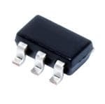
ICGOO电子元器件商城为您提供TPS76433DBVR由Texas Instruments设计生产,在icgoo商城现货销售,并且可以通过原厂、代理商等渠道进行代购。 TPS76433DBVR价格参考¥6.21-¥7.77。Texas InstrumentsTPS76433DBVR封装/规格:PMIC - 稳压器 - 线性, Linear Voltage Regulator IC 1 Output 150mA SOT-23-5。您可以下载TPS76433DBVR参考资料、Datasheet数据手册功能说明书,资料中有TPS76433DBVR 详细功能的应用电路图电压和使用方法及教程。
TPS76433DBVR是Texas Instruments(德州仪器)生产的一款低压差线性稳压器(LDO),属于PMIC - 稳压器 - 线性产品类别。该器件输出电压固定为3.3V,最大输出电流可达150mA,具有低静态电流(典型值为70μA)和优异的负载/线路调整率,采用小型SOT-23-5封装,适合对空间和功耗敏感的应用。

其典型应用场景包括便携式电池供电设备,如智能手机、平板电脑、可穿戴设备和无线传感器节点,得益于低功耗特性,有助于延长电池寿命。此外,TPS76433DBVR具备良好的噪声抑制能力和高电源抑制比(PSRR),适用于为噪声敏感的模拟电路或射频模块(如RF收发器、传感器信号调理电路)提供稳定电源。

在工业控制与通信系统中,该LDO可用于为微控制器(MCU)、低功耗FPGA、ADC/DAC等精密电子元件提供干净的电压源。其热过载保护和短路保护功能增强了系统可靠性,适合在宽温度范围(-40°C 至 125°C)内稳定运行,因此也广泛应用于汽车电子、医疗设备和消费类电子产品中。

总之,TPS76433DBVR凭借小尺寸、低功耗、高稳定性和良好瞬态响应,成为多种中低功率电子系统中理想的电源管理解决方案。
| 参数 | 数值 |
| 产品目录 | 集成电路 (IC)半导体 |
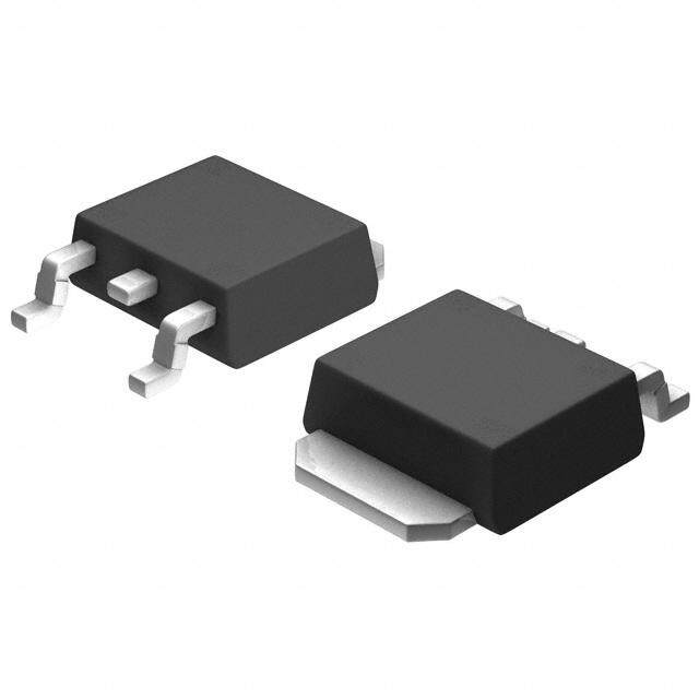
| 描述 | IC REG LDO 3.3V 0.15A SOT23-5低压差稳压器 3.3V 150mA LDO |
| 产品分类 | |
| 品牌 | Texas Instruments |
| 产品手册 | |
| 产品图片 |
|
| rohs | 符合RoHS无铅 / 符合限制有害物质指令(RoHS)规范要求 |
| 产品系列 | 电源管理 IC,低压差稳压器,Texas Instruments TPS76433DBVR- |
| 数据手册 | |
| 产品型号 | TPS76433DBVR |
| 产品目录页面 | |
| 产品种类 | 低压差稳压器 |
| 供应商器件封装 | SOT-23-5 |
| 其它名称 | 296-11028-1 |
| 包装 | 剪切带 (CT) |
| 单位重量 | 13 mg |
| 商标 | Texas Instruments |
| 回动电压—最大值 | 500 mV |
| 安装类型 | 表面贴装 |
| 安装风格 | SMD/SMT |
| 封装 | Reel |
| 封装/外壳 | SC-74A,SOT-753 |
| 封装/箱体 | SOT-23-5 |
| 工作温度 | -40°C ~ 125°C |
| 工厂包装数量 | 3000 |
| 最大功率耗散 | 0.555 W |
| 最大工作温度 | + 125 C |
| 最大输入电压 | 10 V |
| 最小工作温度 | - 40 C |
| 最小输入电压 | + 2.7 V |
| 标准包装 | 1 |
| 电压-跌落(典型值) | 0.3V @ 150mA |
| 电压-输入 | 最高 10V |
| 电压-输出 | 3.3V |
| 电压调节准确度 | 3 % |
| 电流-输出 | 150mA |
| 电流-限制(最小值) | - |
| 稳压器拓扑 | 正,固定式 |
| 稳压器数 | 1 |
| 系列 | TPS76433 |
| 线路调整率 | 0.07 % / V |
| 输入偏压电流—最大 | 0.085 mA |
| 输出电压 | 3.3 V |
| 输出电流 | 150 mA |
| 输出端数量 | 1 Output |
| 输出类型 | Fixed |


- 商务部:美国ITC正式对集成电路等产品启动337调查
- 曝三星4nm工艺存在良率问题 高通将骁龙8 Gen1或转产台积电
- 太阳诱电将投资9.5亿元在常州建新厂生产MLCC 预计2023年完工
- 英特尔发布欧洲新工厂建设计划 深化IDM 2.0 战略
- 台积电先进制程称霸业界 有大客户加持明年业绩稳了
- 达到5530亿美元!SIA预计今年全球半导体销售额将创下新高
- 英特尔拟将自动驾驶子公司Mobileye上市 估值或超500亿美元
- 三星加码芯片和SET,合并消费电子和移动部门,撤换高东真等 CEO
- 三星电子宣布重大人事变动 还合并消费电子和移动部门
- 海关总署:前11个月进口集成电路产品价值2.52万亿元 增长14.8%


PDF Datasheet 数据手册内容提取
TPS76425, TPS76427, TPS76428, TPS76430, TPS76433 LOW-POWER LOW-NOISE 150-mA LOW-DROPOUT LINEAR REGULATORS SLVS180B – MARCH 1999 – REVISED MAY 2001 (cid:0) 150-mA Low Noise, Low-Dropout Regulator DBV PACKAGE (cid:0) (TOP VIEW) Output Voltage: 2.5 V, 2.7 V, 2.8 V, 3.0 V, 3.3 V (cid:0) Output Noise Typically 50 µV IN 1 5 OUT (cid:0) Quiescent Current Typically 85 µA (cid:0) GND 2 Dropout Voltage, Typically 300 mV at 150 mA EN 3 4 BYPASS (cid:0) Thermal Protection (cid:0) Over Current Limitation (cid:0) Less Than 2-µA Quiescent Current in Shutdown Mode (cid:0) –40°C to 125°C Operating Junction Temperature Range (cid:0) 5-Pin SOT-23 (DBV) Package description The TPS764xx family of low-dropout (LDO) voltage regulators offers the benefits of a low noise, low-dropout voltage, low-power operation, and miniaturized package. Additionally, they feature low quiescent current when compared to conventional LDO regulators. Offered in 5-terminal small outline integrated-circuit SOT-23 package, the TPS764xx series devices are ideal for low-noise applications, cost-sensitive designs and applications where board space is at a premium. A combination of new circuit design and process innovation has enabled the usual pnp pass transistor to be replaced by a PMOS pass element. Because the PMOS pass element behaves as a low-value resistor, the dropout voltage is very low—typically 300 mV at 150 mA of load current (TPS76433)—and is directly proportional to the load current. Since the PMOS pass element is a voltage-driven device, the quiescent current is very low (140 µA maximum) and is stable over the entire range of output load current (0 mA to 150 mA). Intended for use in portable systems such as laptops and cellular phones, the low-dropout voltage feature and low-power operation result in a significant increase in system battery operating life. The TPS764xx also features a logic-enabled sleep mode to shut down the regulator, reducing quiescent current to 1 µA maximum at T = 25°C.The TPS764xx is offered in 2.5-V, 2.7-V, 2.8-V, 3.0-V, and 3.3-V fixed-voltages. J AVAILABLE OPTIONS TJ VOLTAGE PACKAGE PART NUMBER SYMBOL 2.5 V TPS76425DBVT† TPS76425DBVR‡ PBJI 2.7 V TPS76427DBVT† TPS76427DBVR‡ PBKI –40°C to 125°C 2.8 V SSOOTT-2233 TPS76428DBVT† TPS76428DBVR‡ PCEI ((DDBBVV)) 3.0 V TPS76430DBVT† TPS76430DBVR‡ PBLI 3.3 V TPS76433DBVT† TPS76433DBVR‡ PBMI †The DBVT passive indicates tape and reel of 250 parts. ‡The DBVR passive indicates tape and reel of 3000 parts. Please be aware that an important notice concerning availability, standard warranty, and use in critical applications of TexasInstruments semiconductor products and disclaimers thereto appears at the end of this data sheet. PRODUCTION DATA information is current as of publication date. Copyright 2001, Texas Instruments Incorporated Products conform to specifications per the terms of Texas Instruments standard warranty. Production processing does not necessarily include testing of all parameters. POST OFFICE BOX 655303 • DALLAS, TEXAS 75265 1
TPS76425, TPS76427, TPS76428, TPS76430, TPS76433 LOW-POWER LOW-NOISE 150-mA LOW-DROPOUT LINEAR REGULATORS SLVS180B – MARCH 1999 – REVISED MAY 2001 functional block diagram TPS76425/ 27/ 28/ 30/ 33 IN OUT EN BYPASS Current Limit / Thermal VREF Protection GND Terminal Functions TERMINAL II//OO DDEESSCCRRIIPPTTIIOONN NAME GND Ground EN I Enable input BYPASS Output bypass capacitor IN I Input supply voltage OUT O Regulated output voltage absolute maximum ratings over operating free-air temperature range (unless otherwise noted)(cid:0) Input voltage range(cid:1)(cid:7)(cid:5)(cid:5)(cid:4)(cid:6)(cid:8)(cid:5)(cid:3)(cid:2) . . . . . . . . . . . . . . . . . . . . . . . . . . . . . . . . . . . . . . . . . . . . . . . . . . . . –0.3 V to 10 V Voltage range at EN . . . . . . . . . . . . . . . . . . . . . . . . . . . . . . . . . . . . . . . . . . . . . . . . . . . . . . . . . . . –0.3 V to V + 0.3 V I Voltage on OUT, . . . . . . . . . . . . . . . . . . . . . . . . . . . . . . . . . . . . . . . . . . . . . . . . . . . . . . . . . . . . . . . . . . . . . . . . . . . . . 7 V Peak output current . . . . . . . . . . . . . . . . . . . . . . . . . . . . . . . . . . . . . . . . . . . . . . . . . . . . . . . . . . . . . . Internally limited ESD rating, HBM . . . . . . . . . . . . . . . . . . . . . . . . . . . . . . . . . . . . . . . . . . . . . . . . . . . . . . . . . . . . . . . . . . . . . . . . . . 2 kV Continuous total power dissipation . . . . . . . . . . . . . . . . . . . . . . . . . . . . . . . . . . . . . . See dissipation rating tables Operating virtual junction temperature range, T . . . . . . . . . . . . . . . . . . . . . . . . . . . . . . . . . . . . . –40°C to 150°C J Storage temperature range, T . . . . . . . . . . . . . . . . . . . . . . . . . . . . . . . . . . . . . . . . . . . . . . . . . . . –65°C to 150°C stg †Stresses beyond those listed under “absolute maximum ratings” may cause permanent damage to the device. These are stress ratings only, and functional operation of the device at these or any other conditions beyond those indicated under “recommended operating conditions” is not implied. Exposure to absolute-maximum-rated conditions for extended periods may affect device reliability. NOTE 1: All voltage values are with respect to network ground terminal. DISSIPATION RATING TABLE DERATING FACTOR TA ≤ 25°C TA = 70°C TA = 85°C BOARD PACKAGE RθJC RθJA ABOVE TA = 25°C POWER RATING POWER RATING POWER RATING Low K‡ DBV 65.8 °C/W 259 °C/W 3.9 mW/°C 386 mW 212 mW 154 mW High K§ DBV 65.8 °C/W 180 °C/W 5.6 mW/°C 555 mW 305 mW 222 mW ‡The JEDEC Low K (1s) board design used to derive this data was a 3 inch x 3 inch, two layer board with 2 ounce copper traces on top of the board. §The JEDEC High K (2s2p) board design used to derive this data was a 3 inch x 3 inch, multilayer board with 1 ounce internal power and ground planes and 2 ounce copper traces on top and bottom of the board. 2 POST OFFICE BOX 655303 • DALLAS, TEXAS 75265
TPS76425, TPS76427, TPS76428, TPS76430, TPS76433 LOW-POWER LOW-NOISE 150-mA LOW-DROPOUT LINEAR REGULATORS SLVS180B – MARCH 1999 – REVISED MAY 2001 recommended operating conditions MIN NOM MAX UNIT Input voltage, VI† 2.7 10 V Continuous output current, IO 0 150 mA Operating junction temperature, TJ –40 125 °C †To calculate the minimum input voltage for your maximum output current, use the following equation: VI(min) = VO(max) + VDO(max load) electrical characteristics over recommended operating free-air temperature range, µ V = V + 1 V, I = 1 mA, EN = IN, C = 4.7 F (unless otherwise noted) I O(typ) O o PARAMETER TEST CONDITIONS MIN TYP MAX UNIT IIOO == 11 mmAA ttoo 110000 mmAA, TTJJ == 2255°°CC 22.4455 22.55 22.5555 IO = 1 mA to 100 mA 2.425 2.5 2.575 TTPPSS7766442255 VV IO = 1 mA to 150 mA, TJ = 25°C 2.438 2.5 2.562 IO = 1 mA to 150 mA 2.407 2.5 2.593 IO = 1 mA to 100 mA, TJ = 25°C 2.646 2.7 2.754 IO = 1 mA to 100 mA 2.619 2.7 2.781 TTPPSS7766442277 VV IO = 1 mA to 150 mA, TJ = 25°C 2.632 2.7 2.768 IO = 1 mA to 150 mA 2.598 2.7 2.8013 IO = 1 mA to 100 mA TJ = 25°C 2.744 2.8 2.856 IO = 1 mA to 150 mA, 2.73 2.8 2.870 VVOO OOuuttpuutt vvoollttaaggee TTPPSS7766442288 VV IO = 1 mA to 150 mA, TJ = 25°C 2.716 2.8 2.884 IO = 1 mA to 150 mA 2.695 2.8 2.905 IO = 1 mA to 100 mA, TJ = 25°C 2.94 3.0 3.06 IO = 1 mA to 100 mA 2.925 3.0 3.075 TTPPSS7766443300 VV IO = 1 mA to 150 mA, TJ = 25°C 2.91 3.0 3.090 IO = 1 mA to 150 mA 2.887 3.0 3.112 IO = 1 mA to 100 mA, TJ = 25°C 3.234 3.3 3.366 IO = 1 mA to 100 mA 3.201 3.3 3.399 TTPPSS7766443333 VV IO = 1 mA to 150 mA, TJ = 25°C 3.218 3.3 3.382 IO = 1 mA to 150 mA 3.177 3.3 3.423 IO = 0 to 150 mA, TJ = 25°C, Quiescent current 85 100 I((QQ)) ((GGNNDD tteerrmmiinnaall ccuurrrreenntt)) See Note 2 IO = 0 to 150 mA, See Note 2 140 µµA EN < 0.5 V, TJ = 25°C 0.5 1 SSttaannddbbyy ccuurrrreenntt EN < 0.5 V 2 Vn Output noise voltage BTJW = = 2 350°C0 ,Hz to 50 kHz, SCeoe = N 1o0t eµ F2, 50 µV Bypass voltage TJ = 25°C 1.192 V PSRR Ripple rejection f = 1 kHz, Co = 10 µF, TJ = 25°C, See Note 2 60 dB Current limit TJ = 25°C See Note 3 0.8 1.5 A NOTES: 2. Minimum IN operating voltage is 2.7 V or VO(typ) + 1 V, whichever is greater. 3. Test condition includes, output voltage VO=0 V and pulse duration = 10 mS. POST OFFICE BOX 655303 • DALLAS, TEXAS 75265 3
TPS76425, TPS76427, TPS76428, TPS76430, TPS76433 LOW-POWER LOW-NOISE 150-mA LOW-DROPOUT LINEAR REGULATORS SLVS180B – MARCH 1999 – REVISED MAY 2001 electrical characteristics over recommended operating free-air temperature range, µ V = V + 1 V, I = 1 mA, EN = IN, C = 4.7 F (unless otherwise noted) (continued) I O(typ) O o PARAMETER TEST CONDITIONS MIN TYP MAX UNIT Output voltagge line reggulation ((∆VOO/VOO)) VO + 1 V < VI ≤ 10 V, VI ≥ 3.5 V, TJ = 25°C 0.04 0.07 %%//VV (see Note 4) VO + 1 V < VI ≤ 10 V, VI ≥ 3.5 V 0.1 VIH EN high level input See Note 2 1.4 2 VV VIL EN low level input See Note 2 0.5 1.2 EN = 0 V –0.01 –0.5 IIII EENN iinnppuutt ccuurrrreenntt µµAA EN = IN –0.01 –0.5 IO = 0 mA, TJ = 25°C 0.2 IO = 1 mA, TJ = 25°C 3 IO = 50 mA, TJ = 25°C 120 150 IO = 50 mA 200 IO = 75 mA, TJ = 25°C 180 225 TTPPSS7766442255 mmVV IO = 75 mA 300 IO = 100 mA, TJ = 25°C 240 300 IO = 100 mA 400 IO = 150 mA, TJ = 25°C 360 450 IO = 150 mA 600 VVDDOO DDrrooppoouutt vvoollttaaggee ((sseeee NNoottee 55)) IO = 0 mA, TJ = 25°C 0.2 IO = 1 mA, TJ = 25°C 3 IO = 50 mA, TJ = 25°C 100 125 IO = 50 mA 166 IO = 75 mA, TJ = 25°C 150 188 TTPPSS7766443333 mmVV IO = 75 mA 250 IO = 100 mA, TJ = 25°C 200 250 IO = 100 mA 333 IO = 150 mA, TJ = 25°C 300 375 IO = 150 mA 500 NOTES: 2. Minimum IN operating voltage is 2.7 V or VO(typ) + 1 V, whichever is greater. 4. If VO < 2.5 V and VImax = 10 V, VImin = 3.5 V: VO(cid:5)VImax(cid:2)3.5 V(cid:6) Line Reg. (mV) (cid:3) (cid:5)%(cid:4)V(cid:6) (cid:0) (cid:0)1000 100 If VO > 2.5 V and VImax = 10 V, VImin = VO + 1 V: VO(cid:5)VImax(cid:2)(cid:5)VO(cid:1)1(cid:6)(cid:6) Line Reg. (mV) (cid:3) (cid:5)%(cid:4)V(cid:6) (cid:0) (cid:0)1000 100 5. Dropout voltage is defined as the differential voltage between VO and VI when VO drops 100 mV below the value measured with VI = VO + 1.0 V. 4 POST OFFICE BOX 655303 • DALLAS, TEXAS 75265
TPS76425, TPS76427, TPS76428, TPS76430, TPS76433 LOW-POWER LOW-NOISE 150-mA LOW-DROPOUT LINEAR REGULATORS SLVS180B – MARCH 1999 – REVISED MAY 2001 TYPICAL CHARACTERISTICS Table of Graphs FIGURE vs Output current 1 VVOO OOuuttppuutt vvoollttaaggee vs Free-air temperature 2, 3, 4 Vn Output noise vs Frequency 5 vs Bypass capacitance 6 VVn OOuuttppuutt nnooiissee vvoollttaaggee vs Load current 7 Zo Output impedance vs Frequency 8 VDO Dropout voltage vs Free-air temperature 9 Ripple rejection vs Frequency 10 Line transient response 11, 13 Load transient response 12, 14 vs Output current 15, 17 CCoommppeennssaattiioonn sseerriieess rreessiissttaannccee ((CCSSRR)) vs Added ceramic capacitance 16, 18 TPS76425 TPS76425 OUTPUT VOLTAGE OUTPUT VOLTAGE vs vs FREE-AIR TEMPERATURE OUTPUT CURRENT 2.505 2.53 VI = 3.5 V VI = 3.5 V CI = CO = 4.7 µF CI = CO = 4.7 µF 2.5 TA = 25°C 2.52 V V Voltage – 2.24.9459 Voltage – 22.5.51 IO = 1 mA – Output O 2.485 – Output O 2.49 IO = 150 mA V V 2.48 2.48 2.475 2.47 0 30 60 90 120 150 180 –55 –35 –15 5 25 45 65 85 105 125 IO – Output Current – mA (Pulse Tested) TA – Free-Air Temperature – °C Figure 1 Figure 2 POST OFFICE BOX 655303 • DALLAS, TEXAS 75265 5
TPS76425, TPS76427, TPS76428, TPS76430, TPS76433 LOW-POWER LOW-NOISE 150-mA LOW-DROPOUT LINEAR REGULATORS SLVS180B – MARCH 1999 – REVISED MAY 2001 TYPICAL CHARACTERISTICS TPS76425 TPS76433 GROUND CURRENT OUTPUT VOLTAGE vs vs FREE-AIR TEMPERATURE FREE-AIR TEMPERATURE 1000 3.34 VI = 6 V VI = 4.3 V CI = CO = 4.7 µF 3.33 IO = 0 mA and 150 mA 3.32 V A – µrrent – 100 Voltage 33.3.31 IO = 1 mA Cu ut nd utp 3.29 u O ro – G O V 3.28 IO = 150 mA 3.27 10 3.26 –55 –35 –15 5 25 45 65 85 105 125 –55 –35 –15 5 25 45 65 85 105 125 TA – Free-Air Temperature – °C TA – Free-Air Temperature – °C Figure 3 Figure 4 OUTPUT NOISE vs OUTPUT NOISE VOLTAGE FREQUENCY vs 3.3 BYPASS CAPACITANCE 80 CO = 10 µF IO = 150 mA f = 10 Hz to 100 kHz Hz CO = 1 µF V 70 TA = 25°C IO = 1 mA µ µV/ ge – 60 Output Noise – 0.33 CIOO = = 1 15 0µ FmA ICOO = = 1 1500 µmFA put Noise Volta 50 ut 40 0.033 O – VO = 3.3 V n C(BYPASS) = 0.1 µF CO = 10 µF V 30 TA = 25°C IO = 1 mA 0 100 1.1 k 10.1 k 100.1 k 20 10–3 10–2 10–1 f – Frequency – Hz Bypass Capacitance – µF Figure 5 Figure 6 6 POST OFFICE BOX 655303 • DALLAS, TEXAS 75265
TPS76425, TPS76427, TPS76428, TPS76430, TPS76433 LOW-POWER LOW-NOISE 150-mA LOW-DROPOUT LINEAR REGULATORS SLVS180B – MARCH 1999 – REVISED MAY 2001 TYPICAL CHARACTERISTICS OUTPUT NOISE VOLTAGE OUTPUT IMPEDANCE vs vs LOAD CURRENT FREQUENCY 70 10 60 V µ – e Ω g 50 – Volta nce e da s 40 e IO = 1 mA Noi mp 1 ut ut I p p ut 30 ut O O V– n CVOO == 21.05 µVF – Zo IO = 150 mA 20 f = 10 Hz to 100 kHz TA = 25°C ECSI =R C=O 1 =Ω 4.7 µF 10 TA = 25°C 0 101 102 0.1 0.01 0.1 1 10 100 1000 Load Current – mA f – Frequency – kHz Figure 7 Figure 8 TPS76425 TPS76425 DROPOUT VOLTAGE RIPPLE REJECTION vs vs FREE-AIR TEMPERATURE FREQUENCY 600 100 VI = EN = 2.7 V VO = 2.5 V CI = CO = 4.7 µF 90 C(BYPASS) = 0.01 µF 500 CL = 10 µF 80 V m e – 400 150 mA – dB 70 ag n 60 IO = 1 mA Volt ctio ut 300 eje 50 o R rop ple 40 IO = 150 mA – D 200 Rip 30 O D 1 mA V 0 mA 20 100 10 0 0 –55 –35 –15 5 25 45 65 85 105 125 10 100 1 k 10 k 100 k 1 M 10 M TA – Free-Air Temperature – °C f – Frequency – Hz Figure 9 Figure 10 POST OFFICE BOX 655303 • DALLAS, TEXAS 75265 7
TPS76425, TPS76427, TPS76428, TPS76430, TPS76433 LOW-POWER LOW-NOISE 150-mA LOW-DROPOUT LINEAR REGULATORS SLVS180B – MARCH 1999 – REVISED MAY 2001 TYPICAL CHARACTERISTICS TPS76425 TPS76425 LINE TRANSIENT RESPONSE LOAD TRANSIENT RESPONSE 200 mA TA = 25°C TA = 25°C 6 V 100 mA 0 mA 4.7 V 50 mV 50 mV 0 0 –50 mV –50 mV –100 mV 0 20 40 60 80 100 120 140 160 180 200 0 20 40 60 80 100 120 140 160 180 200 t – Time – µs t – Time – µs Figure 11 Figure 12 TPS76433 TPS76433 LINE TRANSIENT RESPONSE LOAD TRANSIENT RESPONSE 200 mA TA = 25°C TA = 25°C 6 V 100 mA 0 4.7 V 100 mV 50 mV 50 mV 0 0 –50 mV –50 mV –100 mV dv (cid:0) 1 V µ –150 mV dt 10 s 0 20 40 60 80 100 120 140 160 180 200 0 20 40 60 80 100 120 140 160 180 200 t – Time – µs t – Time – µs Figure 13 Figure 14 8 POST OFFICE BOX 655303 • DALLAS, TEXAS 75265
TPS76425, TPS76427, TPS76428, TPS76430, TPS76433 LOW-POWER LOW-NOISE 150-mA LOW-DROPOUT LINEAR REGULATORS SLVS180B – MARCH 1999 – REVISED MAY 2001 TYPICAL CHARACTERISTICS TYPICAL REGIONS OF STABILITY TYPICAL REGIONS OF STABILITY COMPENSATION SERIES RESISTANCE (CSR)† COMPENSATION SERIES RESISTANCE (CSR)† vs vs OUTPUT CURRENT ADDED CERAMIC CAPACITANCE 100 100 Ω Ω e – Region of Instability e – Region of Instability c c n n a a st 10 st 10 si si e e R R s s e e Seri CO = 4.7 µF Seri I = 150 mA n 1 TA = 25°C n 1 CO = 4.7 µF atio atio TA = 25°C s s n n e e p p m m Co 0.1 Co 0.1 – – R Region of Instability R Region of Instability S S C C 0.01 0.01 0 50 100 150 200 250 0 0.1 0.2 0.3 0.4 0.5 0.6 0.7 0.8 0.9 1 IO – Output Current – mA Added Ceramic Capacitance – µF Figure 15 Figure 16 TYPICAL REGIONS OF STABILITY TYPICAL REGIONS OF STABILITY COMPENSATION SERIES RESISTANCE (CSR)† COMPENSATION SERIES RESISTANCE (CSR)† vs vs OUTPUT CURRENT ADDED CERAMIC CAPACITANCE 100 100 Ω Ω – – e Region of Instability e Region of Instability c c n n a a st 10 st 10 si si e e R R s s e e eri CO = 10 µF eri CO = 10 µF n S 1 n S 1 o o ati ati s s n n e e p p m m o 0.1 o 0.1 C C – Region of Instability – R R Region of Instability S S C C 0.01 0.01 0 50 100 150 200 250 0 0.1 0.2 0.3 0.4 0.5 0.6 0.7 0.8 0.9 1 IO – Output Current – mA Added Ceramic Capacitance – µF Figure 17 Figure 18 †CSR refers to the total series resistance, including the ESR of the capacitor, any series resistance added externally, and PWB trace resistance to CO. POST OFFICE BOX 655303 • DALLAS, TEXAS 75265 9
TPS76425, TPS76427, TPS76428, TPS76430, TPS76433 LOW-POWER LOW-NOISE 150-mA LOW-DROPOUT LINEAR REGULATORS SLVS180B – MARCH 1999 – REVISED MAY 2001 APPLICATION INFORMATION The TPS764xx family of low-noise and low-dropout (LDO) regulators are optimized for use in battery-operated equipment. They feature extremely low noise (50 µV), low dropout voltages, low quiescent current (140 µA), and an enable input to reduce supply current to less than 2 µA when the regulator is turned off. device operation The TPS764xx uses a PMOS pass element to dramatically reduce both dropout voltage and supply current over more conventional PNP-pass-element LDO designs. The PMOS pass element is a voltage-controlled device which, unlike a PNP transistor, does not require increased drive current as output current increases. Supply current in the TPS764xx is essentially constant from no-load to maximum load. Current limiting and thermal protection prevent damage by excessive output current and/or power dissipation. The device switches into a constant-current mode at approximately 1 A; further load reduces the output voltage instead of increasing the output current. The thermal protection shuts the regulator off if the junction temperature rises above 165°C. Recovery is automatic when the junction temperature drops approximately 25°C below the high temperature trip point. The PMOS pass element includes a back diode that safely conducts reverse current when the input voltage level drops below the output voltage level. An internal resistor, in conjunction with external 0.01-µF bypass capacitor, creates a low-pass filter to further reduce the noise. The TPS764xx exhibits only 50 µV of output voltage noise using 0.01 µF bypass and 4.7-µF output capacitors. A logic low on the enable input, EN, shuts off the output and reduces the supply current to less than 2 µA. EN should be tied high in applications where the shutdown feature is not used. A typical application circuit is shown in Figure 19. TPS764xx† 1 VI IN OUT 5 VO C1 4 1 µF 3 BYPASS + EN + 0.01 µF 4.7 µF GND 2 CSR = 1 Ω †TPS76425, TPS76427 TPS76430, TPS76433. Figure 19. Typical Application Circuit 10 POST OFFICE BOX 655303 • DALLAS, TEXAS 75265
TPS76425, TPS76427, TPS76428, TPS76430, TPS76433 LOW-POWER LOW-NOISE 150-mA LOW-DROPOUT LINEAR REGULATORS SLVS180B – MARCH 1999 – REVISED MAY 2001 APPLICATION INFORMATION external capacitor requirements Although not required, a 0.047-µF or larger ceramic bypass input capacitor, connected between IN and GND and located close to the TPS764xx, is recommended to improve transient response and noise rejection. A higher-value electrolytic input capacitor may be necessary if large, fast-rise-time load transients are anticipated and the device is located several inches from the power source. Like all low dropout regulators, the TPS764xx requires an output capacitor connected between OUT and GND to stabilize the internal loop control. The minimum recommended capacitance value is 4.7 µF and the ESR (equivalent series resistance) must be between 0.2 Ω and 10 Ω. Capacitor values 4.7 µF or larger are acceptable, provided the ESR is less than 10 Ω. Solid tantalum electrolytic, aluminum electrolytic, and multilayer ceramic capacitors are all suitable, provided they meet the requirements described above. Most of the commercially available 4.7 µF surface-mount solid tantalum capacitors, including devices from Sprague, Kemet, and Nichico, meet the ESR requirements previously stated. Multilayer ceramic capacitors should have minimum values of 1 µF over the full operating temperature range of the equipment. CAPACITOR SELECTION PART NO. MFR. VALUE MAX ESR† SIZE (H × L × W)† T494B475K016AS KEMET 4.7 µF 1.5 Ω 1.9 × 3.5 × 2.8 195D106x0016x2T SPRAGUE 10 µF 1.5 Ω 1.3 × 7.0 × 2.7 695D106x003562T SPRAGUE 10 µF 1.3 Ω 2.5 × 7.6 × 2.5 TPSC475K035R0600 AVX 4.7 µF 0.6 Ω 2.6 × 6.0 × 3.2 †Size is in mm. ESR is maximum resistance in ohms at 100 kHz and TA = 25°C. Listings are sorted by height. POST OFFICE BOX 655303 • DALLAS, TEXAS 75265 11
TPS76425, TPS76427, TPS76428, TPS76430, TPS76433 LOW-POWER LOW-NOISE 150-mA LOW-DROPOUT LINEAR REGULATORS SLVS180B – MARCH 1999 – REVISED MAY 2001 APPLICATION INFORMATION power dissipation and junction temperature Specified regulator operation is assured to a junction temperature of 125°C; the maximum junction temperature allowable without damaging the device is 150°C. This restriction limits the power dissipation the regulator can handle in any given application. To ensure the junction temperature is within acceptable limits, calculate the maximum allowable dissipation, P , and the actual dissipation, P , which must be less than or equal to D(max) D P . D(max) The maximum-power-dissipation limit is determined using the following equation: (cid:0)TJmax(cid:1)TA P D(max) R (cid:0)JA Where: TJmax is the maximum allowable junction temperature RθJA is the thermal resistance junction-to-ambient for the package, see the dissipation rating table. TA is the ambient temperature. The regulator dissipation is calculated using: PD(cid:2)(cid:3)VI(cid:1)VO(cid:4)(cid:0)IO Power dissipation resulting from quiescent current is negligible. regulator protection The TPS764xx pass element has a built-in back diode that safely conducts reverse current when the input voltage drops below the output voltage (e.g., during power down). Current is conducted from the output to the input and is not internally limited. If extended reverse voltage is anticipated, external limiting might be appropriate. The TPS764xx also features internal current limiting and thermal protection. During normal operation, the TPS764xx limits output current to approximately 800 mA. When current limiting engages, the output voltage scales back linearly until the overcurrent condition ends. While current limiting is designed to prevent gross device failure, care should be taken not to exceed the power dissipation ratings of the package. If the temperature of the device exceeds 165°C, thermal-protection circuitry shuts it down. Once the device has cooled down to below 140°C, regulator operation resumes. 12 POST OFFICE BOX 655303 • DALLAS, TEXAS 75265
TPS76425, TPS76427, TPS76428, TPS76430, TPS76433 LOW-POWER LOW-NOISE 150-mA LOW-DROPOUT LINEAR REGULATORS SLVS180B – MARCH 1999 – REVISED MAY 2001 MECHANICAL DATA DBV (R-PDSO-G5) PLASTIC SMALL-OUTLINE 0,50 0,95 0,20 M 0,30 5 4 0,15 NOM 1,70 3,00 1,50 2,60 1 3 Gage Plane 3,00 2,80 0,25 0°–8° 0,55 0,35 Seating Plane 1,45 0,05 MIN 0,10 0,95 4073253-4/F 10/00 NOTES: A. All linear dimensions are in millimeters. B. This drawing is subject to change without notice. C. Body dimensions do not include mold flash or protrusion. D. Falls within JEDEC MO-178 POST OFFICE BOX 655303 • DALLAS, TEXAS 75265 13
PACKAGE OPTION ADDENDUM www.ti.com 5-Feb-2007 PACKAGING INFORMATION OrderableDevice Status(1) Package Package Pins Package EcoPlan(2) Lead/BallFinish MSLPeakTemp(3) Type Drawing Qty TPS76425DBVR ACTIVE SOT-23 DBV 5 3000 Green(RoHS& CUNIPDAU Level-1-260C-UNLIM noSb/Br) TPS76425DBVRG4 ACTIVE SOT-23 DBV 5 3000 Green(RoHS& CUNIPDAU Level-1-260C-UNLIM noSb/Br) TPS76425DBVT ACTIVE SOT-23 DBV 5 250 Green(RoHS& CUNIPDAU Level-1-260C-UNLIM noSb/Br) TPS76425DBVTG4 ACTIVE SOT-23 DBV 5 250 Green(RoHS& CUNIPDAU Level-1-260C-UNLIM noSb/Br) TPS76427DBVR ACTIVE SOT-23 DBV 5 3000 Green(RoHS& CUNIPDAU Level-1-260C-UNLIM noSb/Br) TPS76427DBVRG4 ACTIVE SOT-23 DBV 5 3000 Green(RoHS& CUNIPDAU Level-1-260C-UNLIM noSb/Br) TPS76427DBVT ACTIVE SOT-23 DBV 5 250 Green(RoHS& CUNIPDAU Level-1-260C-UNLIM noSb/Br) TPS76427DBVTG4 ACTIVE SOT-23 DBV 5 250 Green(RoHS& CUNIPDAU Level-1-260C-UNLIM noSb/Br) TPS76428DBV OBSOLETE SOT-23 DBV 5 TBD CallTI CallTI TPS76428DBVR ACTIVE SOT-23 DBV 5 3000 Green(RoHS& CUNIPDAU Level-1-260C-UNLIM noSb/Br) TPS76428DBVRG4 ACTIVE SOT-23 DBV 5 3000 Green(RoHS& CUNIPDAU Level-1-260C-UNLIM noSb/Br) TPS76428DBVT ACTIVE SOT-23 DBV 5 250 Green(RoHS& CUNIPDAU Level-1-260C-UNLIM noSb/Br) TPS76428DBVTG4 ACTIVE SOT-23 DBV 5 250 Green(RoHS& CUNIPDAU Level-1-260C-UNLIM noSb/Br) TPS76430DBVR ACTIVE SOT-23 DBV 5 3000 Green(RoHS& CUNIPDAU Level-1-260C-UNLIM noSb/Br) TPS76430DBVRG4 ACTIVE SOT-23 DBV 5 3000 Green(RoHS& CUNIPDAU Level-1-260C-UNLIM noSb/Br) TPS76430DBVT ACTIVE SOT-23 DBV 5 250 Green(RoHS& CUNIPDAU Level-1-260C-UNLIM noSb/Br) TPS76430DBVTG4 ACTIVE SOT-23 DBV 5 250 Green(RoHS& CUNIPDAU Level-1-260C-UNLIM noSb/Br) TPS76433DBVR ACTIVE SOT-23 DBV 5 3000 Green(RoHS& CUNIPDAU Level-1-260C-UNLIM noSb/Br) TPS76433DBVRG4 ACTIVE SOT-23 DBV 5 3000 Green(RoHS& CUNIPDAU Level-1-260C-UNLIM noSb/Br) TPS76433DBVT ACTIVE SOT-23 DBV 5 250 Green(RoHS& CUNIPDAU Level-1-260C-UNLIM noSb/Br) TPS76433DBVTG4 ACTIVE SOT-23 DBV 5 250 Green(RoHS& CUNIPDAU Level-1-260C-UNLIM noSb/Br) (1)Themarketingstatusvaluesaredefinedasfollows: ACTIVE:Productdevicerecommendedfornewdesigns. LIFEBUY:TIhasannouncedthatthedevicewillbediscontinued,andalifetime-buyperiodisineffect. NRND:Notrecommendedfornewdesigns.Deviceisinproductiontosupportexistingcustomers,butTIdoesnotrecommendusingthispartin anewdesign. PREVIEW:Devicehasbeenannouncedbutisnotinproduction.Samplesmayormaynotbeavailable. OBSOLETE:TIhasdiscontinuedtheproductionofthedevice. (2)EcoPlan-Theplannedeco-friendlyclassification:Pb-Free(RoHS),Pb-Free(RoHSExempt),orGreen(RoHS&noSb/Br)-pleasecheck Addendum-Page1
PACKAGE OPTION ADDENDUM www.ti.com 5-Feb-2007 http://www.ti.com/productcontentforthelatestavailabilityinformationandadditionalproductcontentdetails. TBD:ThePb-Free/Greenconversionplanhasnotbeendefined. Pb-Free(RoHS):TI'sterms"Lead-Free"or"Pb-Free"meansemiconductorproductsthatarecompatiblewiththecurrentRoHSrequirements forall6substances,includingtherequirementthatleadnotexceed0.1%byweightinhomogeneousmaterials.Wheredesignedtobesoldered athightemperatures,TIPb-Freeproductsaresuitableforuseinspecifiedlead-freeprocesses. Pb-Free(RoHSExempt):ThiscomponenthasaRoHSexemptionforeither1)lead-basedflip-chipsolderbumpsusedbetweenthedieand package, or 2) lead-based die adhesive used between the die and leadframe. The component is otherwise considered Pb-Free (RoHS compatible)asdefinedabove. Green(RoHS&noSb/Br):TIdefines"Green"tomeanPb-Free(RoHScompatible),andfreeofBromine(Br)andAntimony(Sb)basedflame retardants(BrorSbdonotexceed0.1%byweightinhomogeneousmaterial) (3) MSL, Peak Temp. -- The Moisture Sensitivity Level rating according to the JEDEC industry standard classifications, and peak solder temperature. Important Information and Disclaimer:The information provided on this page represents TI's knowledge and belief as of the date that it is provided. TI bases its knowledge and belief on information provided by third parties, and makes no representation or warranty as to the accuracy of such information. Efforts are underway to better integrate information from third parties. TI has taken and continues to take reasonable steps to provide representative and accurate information but may not have conducted destructive testing or chemical analysis on incomingmaterialsandchemicals.TIandTIsuppliersconsidercertaininformationtobeproprietary,andthusCASnumbersandotherlimited informationmaynotbeavailableforrelease. InnoeventshallTI'sliabilityarisingoutofsuchinformationexceedthetotalpurchasepriceoftheTIpart(s)atissueinthisdocumentsoldbyTI toCustomeronanannualbasis. Addendum-Page2
PACKAGE MATERIALS INFORMATION www.ti.com 11-Mar-2008 TAPE AND REEL INFORMATION *Alldimensionsarenominal Device Package Package Pins SPQ Reel Reel A0(mm) B0(mm) K0(mm) P1 W Pin1 Type Drawing Diameter Width (mm) (mm) Quadrant (mm) W1(mm) TPS76425DBVR SOT-23 DBV 5 3000 180.0 9.0 3.15 3.2 1.4 4.0 8.0 Q3 TPS76425DBVT SOT-23 DBV 5 250 180.0 9.0 3.15 3.2 1.4 4.0 8.0 Q3 TPS76427DBVR SOT-23 DBV 5 3000 180.0 9.0 3.15 3.2 1.4 4.0 8.0 Q3 TPS76427DBVT SOT-23 DBV 5 250 180.0 9.0 3.15 3.2 1.4 4.0 8.0 Q3 TPS76428DBVR SOT-23 DBV 5 3000 180.0 9.0 3.15 3.2 1.4 4.0 8.0 Q3 TPS76428DBVT SOT-23 DBV 5 250 180.0 9.0 3.15 3.2 1.4 4.0 8.0 Q3 TPS76430DBVR SOT-23 DBV 5 3000 180.0 9.0 3.15 3.2 1.4 4.0 8.0 Q3 TPS76430DBVT SOT-23 DBV 5 250 180.0 9.0 3.15 3.2 1.4 4.0 8.0 Q3 TPS76433DBVR SOT-23 DBV 5 3000 180.0 9.0 3.15 3.2 1.4 4.0 8.0 Q3 TPS76433DBVT SOT-23 DBV 5 250 180.0 9.0 3.15 3.2 1.4 4.0 8.0 Q3 PackMaterials-Page1
PACKAGE MATERIALS INFORMATION www.ti.com 11-Mar-2008 *Alldimensionsarenominal Device PackageType PackageDrawing Pins SPQ Length(mm) Width(mm) Height(mm) TPS76425DBVR SOT-23 DBV 5 3000 182.0 182.0 20.0 TPS76425DBVT SOT-23 DBV 5 250 182.0 182.0 20.0 TPS76427DBVR SOT-23 DBV 5 3000 182.0 182.0 20.0 TPS76427DBVT SOT-23 DBV 5 250 182.0 182.0 20.0 TPS76428DBVR SOT-23 DBV 5 3000 182.0 182.0 20.0 TPS76428DBVT SOT-23 DBV 5 250 182.0 182.0 20.0 TPS76430DBVR SOT-23 DBV 5 3000 182.0 182.0 20.0 TPS76430DBVT SOT-23 DBV 5 250 182.0 182.0 20.0 TPS76433DBVR SOT-23 DBV 5 3000 182.0 182.0 20.0 TPS76433DBVT SOT-23 DBV 5 250 182.0 182.0 20.0 PackMaterials-Page2
IMPORTANTNOTICE TexasInstrumentsIncorporatedanditssubsidiaries(TI)reservetherighttomakecorrections,modifications,enhancements,improvements, andotherchangestoitsproductsandservicesatanytimeandtodiscontinueanyproductorservicewithoutnotice.Customersshould obtainthelatestrelevantinformationbeforeplacingordersandshouldverifythatsuchinformationiscurrentandcomplete.Allproductsare soldsubjecttoTI’stermsandconditionsofsalesuppliedatthetimeoforderacknowledgment. TIwarrantsperformanceofitshardwareproductstothespecificationsapplicableatthetimeofsaleinaccordancewithTI’sstandard warranty.TestingandotherqualitycontroltechniquesareusedtotheextentTIdeemsnecessarytosupportthiswarranty.Exceptwhere mandatedbygovernmentrequirements,testingofallparametersofeachproductisnotnecessarilyperformed. TIassumesnoliabilityforapplicationsassistanceorcustomerproductdesign.Customersareresponsiblefortheirproductsand applicationsusingTIcomponents.Tominimizetherisksassociatedwithcustomerproductsandapplications,customersshouldprovide adequatedesignandoperatingsafeguards. TIdoesnotwarrantorrepresentthatanylicense,eitherexpressorimplied,isgrantedunderanyTIpatentright,copyright,maskworkright, orotherTIintellectualpropertyrightrelatingtoanycombination,machine,orprocessinwhichTIproductsorservicesareused.Information publishedbyTIregardingthird-partyproductsorservicesdoesnotconstitutealicensefromTItousesuchproductsorservicesora warrantyorendorsementthereof.Useofsuchinformationmayrequirealicensefromathirdpartyunderthepatentsorotherintellectual propertyofthethirdparty,oralicensefromTIunderthepatentsorotherintellectualpropertyofTI. ReproductionofTIinformationinTIdatabooksordatasheetsispermissibleonlyifreproductioniswithoutalterationandisaccompanied byallassociatedwarranties,conditions,limitations,andnotices.Reproductionofthisinformationwithalterationisanunfairanddeceptive businesspractice.TIisnotresponsibleorliableforsuchaltereddocumentation.Informationofthirdpartiesmaybesubjecttoadditional restrictions. ResaleofTIproductsorserviceswithstatementsdifferentfromorbeyondtheparametersstatedbyTIforthatproductorservicevoidsall expressandanyimpliedwarrantiesfortheassociatedTIproductorserviceandisanunfairanddeceptivebusinesspractice.TIisnot responsibleorliableforanysuchstatements. TIproductsarenotauthorizedforuseinsafety-criticalapplications(suchaslifesupport)whereafailureoftheTIproductwouldreasonably beexpectedtocauseseverepersonalinjuryordeath,unlessofficersofthepartieshaveexecutedanagreementspecificallygoverning suchuse.Buyersrepresentthattheyhaveallnecessaryexpertiseinthesafetyandregulatoryramificationsoftheirapplications,and acknowledgeandagreethattheyaresolelyresponsibleforalllegal,regulatoryandsafety-relatedrequirementsconcerningtheirproducts andanyuseofTIproductsinsuchsafety-criticalapplications,notwithstandinganyapplications-relatedinformationorsupportthatmaybe providedbyTI.Further,BuyersmustfullyindemnifyTIanditsrepresentativesagainstanydamagesarisingoutoftheuseofTIproductsin suchsafety-criticalapplications. TIproductsareneitherdesignednorintendedforuseinmilitary/aerospaceapplicationsorenvironmentsunlesstheTIproductsare specificallydesignatedbyTIasmilitary-gradeor"enhancedplastic."OnlyproductsdesignatedbyTIasmilitary-grademeetmilitary specifications.BuyersacknowledgeandagreethatanysuchuseofTIproductswhichTIhasnotdesignatedasmilitary-gradeissolelyat theBuyer'srisk,andthattheyaresolelyresponsibleforcompliancewithalllegalandregulatoryrequirementsinconnectionwithsuchuse. TIproductsareneitherdesignednorintendedforuseinautomotiveapplicationsorenvironmentsunlessthespecificTIproductsare designatedbyTIascompliantwithISO/TS16949requirements.Buyersacknowledgeandagreethat,iftheyuseanynon-designated productsinautomotiveapplications,TIwillnotberesponsibleforanyfailuretomeetsuchrequirements. FollowingareURLswhereyoucanobtaininformationonotherTexasInstrumentsproductsandapplicationsolutions: Products Applications Amplifiers amplifier.ti.com Audio www.ti.com/audio DataConverters dataconverter.ti.com Automotive www.ti.com/automotive DSP dsp.ti.com Broadband www.ti.com/broadband ClocksandTimers www.ti.com/clocks DigitalControl www.ti.com/digitalcontrol Interface interface.ti.com Medical www.ti.com/medical Logic logic.ti.com Military www.ti.com/military PowerMgmt power.ti.com OpticalNetworking www.ti.com/opticalnetwork Microcontrollers microcontroller.ti.com Security www.ti.com/security RFID www.ti-rfid.com Telephony www.ti.com/telephony RF/IFandZigBee®Solutions www.ti.com/lprf Video&Imaging www.ti.com/video Wireless www.ti.com/wireless MailingAddress:TexasInstruments,PostOfficeBox655303,Dallas,Texas75265 Copyright©2008,TexasInstrumentsIncorporated