ICGOO在线商城 > 集成电路(IC) > PMIC - 稳压器 - 线性 > LD1085D2M25R

 Datasheet下载
- 型号: LD1085D2M25R
- 制造商: STMicroelectronics
- 库位|库存: xxxx|xxxx
- 要求:
| 数量阶梯 | 香港交货 | 国内含税 |
| +xxxx | $xxxx | ¥xxxx |
查看当月历史价格
查看今年历史价格
LD1085D2M25R产品简介:
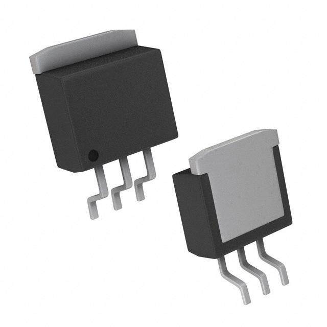
ICGOO电子元器件商城为您提供LD1085D2M25R由STMicroelectronics设计生产,在icgoo商城现货销售,并且可以通过原厂、代理商等渠道进行代购。 LD1085D2M25R价格参考。STMicroelectronicsLD1085D2M25R封装/规格:PMIC - 稳压器 - 线性, Linear Voltage Regulator IC Positive Fixed 1 Output 2.5V 3A D2PAK-3。您可以下载LD1085D2M25R参考资料、Datasheet数据手册功能说明书,资料中有LD1085D2M25R 详细功能的应用电路图电压和使用方法及教程。
STMicroelectronics的LD1085D2M25R是一款线性稳压器,属于PMIC(电源管理集成电路)类别。该型号的应用场景主要包括以下几个方面:

 1. 消费电子设备
   - 便携式设备:如移动电源、蓝牙音箱、智能手环等需要稳定电压输出的设备。
   - 音频设备:例如耳机放大器、便携式音响等,提供低噪声电源以改善音质。
   - 智能家居产品:如智能灯泡、智能插座等,确保其微控制器和传感器的供电稳定性。

 2. 工业应用
   - 传感器模块:为温度、湿度、压力等传感器提供稳定的电源,确保测量精度。
   - 嵌入式系统:用于工业控制板卡或小型化嵌入式设备中,为其处理器或接口电路供电。
   - 通信模块:如RS-485、CAN总线模块等,保证通信信号的可靠性。

 3. 医疗设备
   - 便携式医疗仪器:如血糖仪、脉搏血氧仪等,需要低功耗和高精度电源。
   - 健康监测设备:如心率监测器、睡眠监测器等,提供稳定的低压电源支持。

 4. 汽车电子
   - 车载辅助设备:如倒车摄像头、行车记录仪等,适用于需要宽输入电压范围的场景。
   - 车内娱乐系统:如音频放大器、显示屏等,确保其正常工作。

 5. 物联网(IoT)设备
   - 无线模块:如Wi-Fi、Zigbee、LoRa等模块,为射频芯片提供干净的电源。
   - 数据采集终端:如环境监测节点、农业自动化设备等,确保长时间稳定运行。

 特点与优势
- 高精度输出:LD1085D2M25R能够提供2.25V的固定输出电压,适合对电压要求严格的场合。
- 低dropout特性:允许在较低的输入电压下工作,提高效率并减少热量产生。
- 过流保护和热关断功能:增强系统的可靠性和安全性。
- 小尺寸封装:TO-252(DPAK)封装节省空间,适合紧凑型设计。

总之,LD1085D2M25R适用于需要高效、低噪声、稳定电压输出的各种电子设备,尤其在对功耗和散热有较高要求的场景中表现出色。
| 参数 | 数值 |
| 产品目录 | 集成电路 (IC)半导体 |
| 描述 | IC REG LDO 2.5V 3A D2PAK低压差稳压器 2.5V 3.0A Positive |
| 产品分类 | |
| 品牌 | STMicroelectronics |
| 产品手册 | |
| 产品图片 |
|
| rohs | 符合RoHS无铅 / 符合限制有害物质指令(RoHS)规范要求 |
| 产品系列 | 电源管理 IC,低压差稳压器,STMicroelectronics LD1085D2M25R- |
| 数据手册 | |
| 产品型号 | LD1085D2M25R |
| 产品目录页面 | |
| 产品种类 | 低压差稳压器 |
| 供应商器件封装 | D2PAK-3 |
| 其它名称 | 497-3422-1 |
| 其它有关文件 | http://www.st.com/web/catalog/sense_power/FM142/CL1015/SC312/PF63439?referrer=70071840http://www.st.com/web/catalog/sense_power/FM142/CL1015/SC312/SS1733/PF63439?referrer=70071840 |
| 包装 | 剪切带 (CT) |
| 商标 | STMicroelectronics |
| 回动电压—最大值 | 1.5 V at 3 A |
| 安装类型 | 表面贴装 |
| 安装风格 | SMD/SMT |
| 封装 | Reel |
| 封装/外壳 | TO-263-4,D²Pak(3 引线+接片),TO-263AA |
| 封装/箱体 | D2PAK |
| 工作温度 | -40°C ~ 125°C |
| 工厂包装数量 | 1000 |
| 最大工作温度 | + 125 C |
| 最大输入电压 | 30 V |
| 最小工作温度 | - 40 C |
| 标准包装 | 1 |
| 电压-跌落(典型值) | 1.3V @ 3A |
| 电压-输入 | 最高 30V |
| 电压-输出 | 2.5V |
| 电压调节准确度 | 1 % |
| 电流-输出 | 3A |
| 电流-限制(最小值) | - |
| 稳压器拓扑 | 正,固定式 |
| 稳压器数 | 1 |
| 系列 | LD1085D2M |
| 线路调整率 | 4 mV |
| 负载调节 | 10 mV |
| 输入偏压电流—最大 | 5 mA |
| 输出电压 | 2.5 V |
| 输出电流 | 3 A |
| 输出端数量 | 1 Output |
| 输出类型 | Fixed |


- 商务部:美国ITC正式对集成电路等产品启动337调查
- 曝三星4nm工艺存在良率问题 高通将骁龙8 Gen1或转产台积电
- 太阳诱电将投资9.5亿元在常州建新厂生产MLCC 预计2023年完工
- 英特尔发布欧洲新工厂建设计划 深化IDM 2.0 战略
- 台积电先进制程称霸业界 有大客户加持明年业绩稳了
- 达到5530亿美元!SIA预计今年全球半导体销售额将创下新高
- 英特尔拟将自动驾驶子公司Mobileye上市 估值或超500亿美元
- 三星加码芯片和SET,合并消费电子和移动部门,撤换高东真等 CEO
- 三星电子宣布重大人事变动 还合并消费电子和移动部门
- 海关总署:前11个月进口集成电路产品价值2.52万亿元 增长14.8%


PDF Datasheet 数据手册内容提取
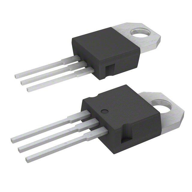
LD1085 3 A low drop positive voltage regulator: adjustable and fixed Datasheet - production data Unlike PNP regulators, where a part of the output current is wasted as quiescent current, the LD1085 quiescent current flows into the load, thus increase efficiency. Only a 10 µF minimum capacitor is need for stability. The device is supplied in TO-220, TO-220FP, D²PAK and D²PAK/A packages. On-chip trimming TO-220 TO-220FP allows the regulator to reach a very tight output voltage tolerance, within ± 1% at 25 °C. D²PAK D²PAK/A Features • Typical dropout 1.3 V (at 3 A) • Three terminal adjustable or fixed output voltage 1.8 V, 2.5 V, 3.3 V, 5 V • Guaranteed output current up to 3 A • Output tolerance ± 1% at 25 °C and ± 2% in full temperature range • Internal power and thermal limit • Wide operating temperature range -40 °C to 125 °C • Package available: TO-220, TO-220FP, D²PAK, D²PAK/A • Pinout compatibility with standard adjustable VREG Description The LD1085 is a low drop voltage regulator able to provide up to 3 A of output current. Dropout is guaranteed at a maximum of 1.2 V at the maximum output current, decreasing at lower loads. The LD1085 is pin-to-pin compatible with the older 3-terminal adjustable regulators, but offers better performance in terms of drop and output tolerance. October 2013 DocID6738 Rev 27 1/27 This is information on a product in full production. www.st.com 27
Contents LD1085 Contents 1 Diagram . . . . . . . . . . . . . . . . . . . . . . . . . . . . . . . . . . . . . . . . . . . . . . . . . . . 3 2 Pin configuration . . . . . . . . . . . . . . . . . . . . . . . . . . . . . . . . . . . . . . . . . . . . 4 3 Maximum ratings . . . . . . . . . . . . . . . . . . . . . . . . . . . . . . . . . . . . . . . . . . . . 5 4 Application schematic . . . . . . . . . . . . . . . . . . . . . . . . . . . . . . . . . . . . . . . 6 5 Electrical characteristics . . . . . . . . . . . . . . . . . . . . . . . . . . . . . . . . . . . . . 7 6 Typical characteristics . . . . . . . . . . . . . . . . . . . . . . . . . . . . . . . . . . . . . . 12 7 Package mechanical data . . . . . . . . . . . . . . . . . . . . . . . . . . . . . . . . . . . . 16 8 Packaging mechanical data . . . . . . . . . . . . . . . . . . . . . . . . . . . . . . . . . . 23 9 Order codes . . . . . . . . . . . . . . . . . . . . . . . . . . . . . . . . . . . . . . . . . . . . . . 26 10 Revision history . . . . . . . . . . . . . . . . . . . . . . . . . . . . . . . . . . . . . . . . . . . 27 2/27 DocID6738 Rev 27
LD1085 Diagram 1 Diagram Figure 1. Schematic diagram DocID6738 Rev 27 3/27
Pin configuration LD1085 2 Pin configuration Figure 2. Pin connections (top view) TO-220 TO-220FP D²PAK D²PAK/A 4/27 DocID6738 Rev 27
LD1085 Maximum ratings 3 Maximum ratings Table 1. Absolute maximum ratings Symbol Parameter Value Unit V DC input voltage 30 V I I Output current Internally limited mA O P Power dissipation Internally limited mW D T Storage temperature range -55 to +150 °C STG T Operating junction temperature range -40 to +125 °C OP Note: Absolute maximum ratings are those values beyond which damage to the device may occur. Functional operation under these condition is not implied Table 2. Thermal data D²PAK Symbol Parameter TO-220 TO-220FP Unit D²PAK/A R Thermal resistance junction-case 3 5 3 °C/W thJC R Thermal resistance junction-ambient 50 60 62.5 °C/W thJA DocID6738 Rev 27 5/27
Application schematic LD1085 4 Application schematic Figure 3. Application circuit R V = V ⋅1+-----2-- O REF R 1 6/27 DocID6738 Rev 27
LD1085 Electrical characteristics 5 Electrical characteristics V = 4.8 V, C = C =10 µF, T = -40 to 125 °C, unless otherwise specified. I I O A Table 3. Electrical characteristics of LD1085#18 Symbol Parameter Test condition Min. Typ. Max. Unit I = 0 mA, T = 25°C 1.782 1.8 1.818 V V Output voltage (1) O J O I = 0 to 3 A, V = 3.4 to 30 V 1.764 1.8 1.836 V O I I = 0 mA, V = 3.4 to 18 V T = 25°C 0.2 4 mV ΔV Line regulation O I J O I = 0 mA, V = 3.4 to 15 V 0.4 4 mV O I I = 0 to 3 A, T = 25°C 2 10 mV ΔV Load regulation O J O I = 0 to 3 A 4 20 mV O V Dropout voltage I = 3 A 1.3 1.5 V d O I Quiescent current V ≤ 30 V 5 10 mA q I V - V = 5 V 3.2 4.5 A I O I Short-circuit current sc V - V = 25 V 0.2 0.5 A I O Thermal regulation T = 25°C, 30 ms pulse 0.008 0.04 %/W A f = 120 Hz, C = 25 µF, I = 3 A SVR Supply voltage rejection O O 60 72 dB V = 7.5 ± 3 V I RMS output noise voltage (% of eN T = 25°C, f =10 Hz to 10 kHz 0.003 % V ) A O S Temperature stability 0.5 % S Long term stability T = 125°C, 1000 Hrs 0.5 % A 1. See short-circuit current curve for available output current at fixed dropout. DocID6738 Rev 27 7/27
Electrical characteristics LD1085 V = 5.5 V, C = C =10 µF, T = -40 to 125 °C, unless otherwise specified. I I O A Table 4. Electrical characteristics of LD1085#25 Symbol Parameter Test condition Min. Typ. Max. Unit I = 0 mA, T = 25°C 2.475 2.5 2.525 V V Output voltage (1) O J O I = 0 to 3 A, V = 4.1 to 30 V 2.45 2.5 2.55 V O I I = 0 mA, V = 4.1 to 18 V, T = 25°C 0.2 4 mV ΔV Line regulation O I J O I = 0 mA, V = 4.1 to 18 V 0.4 4 mV O I I = 0 to 3 A, T = 25°C 2 10 mV ΔV Load regulation O J O I = 0 to 3 A 4 20 mV O V Dropout voltage I = 3 A 1.3 1.5 V d O I Quiescent current V ≤ 30 V 5 10 mA q I V - V = 5 V 3.2 4.5 A I O I Short-circuit current sc V - V = 25 V 0.2 0.5 A I O Thermal regulation T = 25°C, 30ms pulse 0.008 0.04 %/W A f = 120 Hz, C = 25µF, I = 3 A SVR Supply voltage rejection O O 60 72 dB V = 7.5 ± 3 V I RMS output noise voltage (% eN T = 25°C, f =10 Hz to 10 kHz 0.003 % of V ) A O S Temperature stability 0.5 % S Long term stability T = 125°C, 1000 Hrs 0.5 % A 1. See short-circuit current curve for available output current at fixed dropout. 8/27 DocID6738 Rev 27
LD1085 Electrical characteristics V = 6.3 V, C = C =10 µF, T = -40 to 125 °C, unless otherwise specified. I I O A Table 5. Electrical characteristics of LD1085#33 Symbol Parameter Test condition Min. Typ. Max. Unit I = 0 mA, T = 25°C 3.267 3.3 3.333 V V Output voltage (1) O J O I = 0 to 3 A, V = 4.9 to 30 V 3.234 3.35 3.366 V O I I = 0 mA, V = 4.9 to 18 V, T = 25°C 0.5 6 mV ΔV Line regulation O I J O I = 0 mA, V = 4.9 to 18 V 1 6 mV O I I = 0 to 3 A, T = 25°C 3 15 mV ΔV Load regulation O J O I = 0 to 3 A 7 20 mV O V Dropout voltage I = 3 A 1.3 1.5 V d O I Quiescent current V ≤ 30 V 5 10 mA q I V - V = 5 V 3.2 4.5 A I O I Short-circuit current sc V - V = 25 V 0.2 0.5 A I O Thermal regulation T = 25°C, 30 ms pulse 0.008 0.04 %/W A f = 120 Hz, C = 25 µF, I = 3 A SVR Supply voltage rejection O O 60 72 dB V = 8.3 ± 3 V I RMS output noise voltage (% eN T = 25°C, f =10 Hz to 10 kHz 0.003 % of V ) A O S Temperature stability 0.5 % S Long term stability T = 125°C, 1000 Hrs 0.5 % A 1. See short-circuit current curve for available output current at fixed dropout. DocID6738 Rev 27 9/27
Electrical characteristics LD1085 V = 8 V, C = C =10 µF, T = -40 to 125 °C, unless otherwise specified. I I O A Table 6. Electrical characteristics of LD1085#50 Symbol Parameter Test condition Min. Typ. Max. Unit I = 0 mA, T = 25°C 4.95 5 5.05 V V Output voltage (1) O J O I = 0 to 3 A, V = 6.6 to 30 V 4.9 5 5.1 V O I I = 0 mA, V = 6.6 to 20 V, T = 25°C 0.5 10 mV ΔV Line regulation O I J O I = 0 mA, V = 6.6 to 20 V 1 10 mV O I I = 0 to 3 A, T = 25°C 5 10 mV ΔV Load regulation O J O I = 0 to 3 A 10 35 mV O V Dropout voltage I = 3 A 1.3 1.5 V d O I Quiescent current V ≤ 30 V 5 10 mA q I V - V = 5 V 3.2 4.5 A I O I Short-circuit current sc V - V = 25 V 0.2 0.5 A I O Thermal regulation T = 25°C, 30 ms pulse 0.008 0.04 %/W A f = 120 Hz, C = 25 µF, I = 3 A SVR Supply voltage rejection O O 60 72 dB V = 10 ± 3 V I RMS output noise voltage (% eN T = 25°C, f = 10 Hz to 10 kHz 0.003 % of V ) A O S Temperature stability 0.5 % S Long term stability T = 125°C, 1000 Hrs 0.5 % A 1. See short-circuit current curve for available output current at fixed dropout. 10/27 DocID6738 Rev 27
LD1085 Electrical characteristics V = 4.25 V, C = C =10 µF, T = -40 to 125 °C, unless otherwise specified. I I O A Table 7. Electrical characteristics of LD1085# Symbol Parameter Test condition Min. Typ. Max. Unit I = 10 mA T = 25°C 1.237 1.25 1.263 V V Reference voltage (1) O J ref I = 10 mA to 3 A, V = 2.85 to 30 V 1.225 1.25 1.275 V O I I = 10 mA, V = 2.85 to 16.5 V, O I 0.015 0.2 % ΔVO Line regulation TJ = 25°C I = 10 mA, V = 2.85 to 16.5 V 0.035 0.2 % O I I = 10 mA to 3 A, T = 25°C 0.1 0.3 % ΔV Load regulation O J O I = 0 to 3 A 0.2 0.4 % O V Dropout voltage I = 3 A 1.3 1.5 V d O I Minimum load current V = 30 V 3 10 mA O(min) I V - V = 5 V 5.5 6.5 A I O I Short-circuit current sc V - V = 25 V 0.5 0.7 A I O Thermal regulation T = 25°C, 30ms pulse 0.003 0.015 %/W A f = 120 Hz, C = 25 µF,C = 25 µF, SVR Supply voltage rejection O ADJ 60 72 dB I = 3 A, V = 6.25 ± 3 V O I I Adjust pin current V = 4.25 V, I = 10 mA 55 120 µA ADJ I O ΔI Adjust pin current change (1) I = 10 mA to 3 A, V = 2.85 to 16.5 V 0.2 5 µA ADJ O I RMS output noise voltage (% eN T = 25°C, f =10 Hz to 10 kHz 0.003 % of V ) A O S Temperature stability 0.5 % S Long term stability T = 125°C, 1000 Hrs 0.5 % A 1. See short-circuit current curve for available output current at fixed dropout. DocID6738 Rev 27 11/27
Typical characteristics LD1085 6 Typical characteristics Unless otherwise specified T = 25 °C, C = C = 10 µF. J I O Figure 4. O utput voltage vs. temp. (I = 3 A) Figure 5. Output voltage vs. temp. (I = 0 mA) O O Figure 6. Output voltage vs. temp. (I = 10 mA) Figure 7. Short-circuit current vs. dropout O voltage 12/27 DocID6738 Rev 27
LD1085 Typical characteristics Figure 8. Line regulation vs. temp. (I = 10 mA) Figure 9. Load regulation vs. temperature O Figure 10 . Dropout voltage vs. temperature Figure 11. Dropout voltage vs. output current Figure 12. Adjust pin current vs. temperature Figure 13. Quiescent current vs. temperature DocID6738 Rev 27 13/27
Typical characteristics LD1085 Figure 14. Line regulation vs. temperature Figure 15. Supply voltage rejection vs. output (V = 15 V) current IN Figure 1 6. Supply voltage rejection vs. Figure 17. Supply voltage rejection vs. frequency temperature Figure 18. Minimum load current vs. Figure 19. Stability, V = 1.8 V O temperature 14/27 DocID6738 Rev 27
LD1085 Typical characteristics Figure 20. Stability, V = 12 V Figure 21. Line transient O V=12 to 13V, I =200mA, C = 1µF(tant), I O I C =10µF(tant), C =1µF O ADJ F igure 22. Load transient Figure 23. Load transient (No C ) ADJ V=12V, I =0.12 to 3A, C = 1µF(tant), V=12V, I =0.12 to 3A, C = 1µF(tant), I O I I O I C =10µF(tant), C =1µF C =10µF(tant), no C O ADJ O ADJ DocID6738 Rev 27 15/27
Package mechanical data LD1085 7 Package mechanical data In order to meet environmental requirements, ST offers these devices in different grades of ECOPACK® packages, depending on their level of environmental compliance. ECOPACK® specifications, grade definitions and product status are available at: www.st.com. ECOPACK® is an ST trademark. Table 8. TO-220 mechanical data mm Dim. Min. Typ. Max. A 4.40 4.60 b 0.61 0.88 b1 1.14 1.70 c 0.48 0.70 D 15.25 15.75 E 10 10.40 e 2.40 2.70 e1 4.95 5.15 F 0.51 0.60 H1 6.20 6.60 J1 2.40 2.72 L 13 14 L1 3.50 3.93 L20 16.40 L30 28.90 ∅ P 3.75 3.85 Q 2.65 2.95 16/27 DocID6738 Rev 27
LD1085 Package mechanical data Figure 24. TO-220 drawing (cid:27)(cid:20)(cid:26)(cid:23)(cid:25)(cid:21)(cid:26)(cid:66)(cid:85)(cid:72)(cid:89)(cid:39) DocID6738 Rev 27 17/27
Package mechanical data LD1085 Table 9. TO-220FP mechanical data mm Dim. Min. Typ. Max. A 4.4 4.6 B 2.5 2.7 D 2.5 2.75 E 0.45 0.7 F 0.75 1 F1 1.15 1.70 F2 1.15 1.70 G 4.95 5.2 G1 2.4 2.7 H 10 10.4 L2 16 L3 28.6 30.6 L4 9.8 10.6 L5 2.9 3.6 L6 15.9 16.4 L7 9 9.3 Dia 3 3.2 Figure 25. TO-220FP drawing L7 E A B D Dia L5 L6 F1 F2 F H G G1 L2 L4 L3 7012510_Rev_K 18/27 DocID6738 Rev 27
LD1085 Package mechanical data Table 10. D²PAK mechanical data mm Dim. Min. Typ. Max. A 4.40 4.60 A1 0.03 0.23 b 0.70 0.93 b2 1.14 1.70 c 0.45 0.60 c2 1.23 1.36 D 8.95 9.35 D1 7.50 E 10 10.40 E1 8.50 e 2.54 e1 4.88 5.28 H 15 15.85 J1 2.49 2.69 L 2.29 2.79 L1 1.27 1.40 L2 1.30 1.75 R 0.4 V2 0° 8° DocID6738 Rev 27 19/27
Package mechanical data LD1085 Figure 26. D²PAK drawing 0079457_T 20/27 DocID6738 Rev 27
LD1085 Package mechanical data Table 11. D²PAK/A mechanical data mm Dim. Min. Typ. Max. A 4.40 4.60 A1 0.03 0.23 b 0.70 0.93 b2 1.14 1.70 c 0.45 0.60 c2 1.23 1.36 D 8.95 9.35 D1 7.50 E 10 10.40 E1 8.50 e 2.54 e1 4.88 5.28 H 15 15.85 J1 2.49 2.69 L 2.29 2.79 L1 1.27 1.40 R 0.4 V2 0° 8° DocID6738 Rev 27 21/27
Package mechanical data LD1085 Figure 27. D²PAK/A mechanical data 7106164_E 22/27 DocID6738 Rev 27
LD1085 Packaging mechanical data 8 Packaging mechanical data Table 12. D²PAK, D²PAK/A tape and reel mechanical data Tape Reel mm mm Dim. Dim. Min. Max. Min. Max. A0 10.5 10.7 A 330 B0 15.7 15.9 B 1.5 D 1.5 1.6 C 12.8 13.2 D1 1.59 1.61 D 20.2 E 1.65 1.85 G 24.4 26.4 F 11.4 11.6 N 100 K0 4.8 5.0 T 30.4 P0 3.9 4.1 P1 11.9 12.1 Base qty 1000 P2 1.9 2.1 Bulk qty 1000 R 50 T 0.25 0.35 W 23.7 24.3 Figure 28. D²PAK, D²PAK/A footprint(a) 16.90 12.20 5.08 1.60 3.50 9.75 Footprint a. All dimensions are in millimeters DocID6738 Rev 27 23/27
Packaging mechanical data LD1085 Figure 29. Tape for D²PAK and D²PAK/A 10 pitches cumulative tolerance on tape +/- 0.2 mm Top cover P0 D P2 T tape E F K0 W B1 B0 For machine ref. only A0 P1 D1 including draft and radii concentric around B0 User direction of feed R Bending radius User direction of feed AM08852v1 Figure 30. Reel for D²PAK and D²PAK/A T REEL DIMENSIONS 40mm min. Access hole At sl ot location B D C N A Full radius Tape slot G measured at hub in core for tape start 25 mm min. width AM08851v2 24/27 DocID6738 Rev 27
LD1085 Order codes 9 Order codes Table 13. Order codes Packages Output voltage TO-220 TO-220FP D²PAK D²PAK/A (T&R) LD1085D2M18R 1.8 V LD1085D2M25R 2.5 V LD1085D2T33R LD1085D2M33R 3.3 V LD1085V50 5.0 V LD1085V LD1085P LD1085D2T-R LD1085D2M-R ADJ DocID6738 Rev 27 25/27
Revision history LD1085 10 Revision history Table 14. Document revision history Date Revision Changes 07-Oct-2004 12 Mistake order codes - Table 1. 08-Feb-2005 13 Mistake U.M. load regulation - V ==> mV. 01-Mar-2005 14 Version 1.2 V removed. 22-May-2006 15 Order codes has been updated and new template. 10-Nov-2006 16 Add package DPAK, typo on V test value in tables 3, 4 and 11. O 04-Apr-2007 17 Order codes updated. 07-Jun-2007 18 Order codes updated. 05-Dec-2007 19 Modified: Table13. Added new order codes for Automotive grade products see Table13 on 29-Jan-2008 20 page25. 18-Feb-2008 21 Modified: Table13 on page25. 09-Apr-2008 22 Modified: Table13 on page25. 14-Jul-2008 23 Modified: Table13 on page25. 22-Aug-2008 24 Modified: Table2 on page5. 28-Jul-2009 25 Modified: Table13 on page25. – Modified Output voltage in Voltage reference parameter Table7 on page11 18-Feb-2013 26 and Table8 on page12. – Minor text changes throughout the document. RPN LD1085xx changed to LD1085. Updated the Features and the Description in cover page. Cancelled Table1: Device summary, Table 9: Electrical characteristics of LD1085PY (Automotive Grade). 08-Oct-2013 27 Modified Figure2: Pin connections (top view), Table2: Thermal data, Table13: Order codes, Section7: Package mechanical data. Added Section8: Packaging mechanical data. Minor text changes. 26/27 DocID6738 Rev 27
LD1085 Please Read Carefully: Information in this document is provided solely in connection with ST products. STMicroelectronics NV and its subsidiaries (“ST”) reserve the right to make changes, corrections, modifications or improvements, to this document, and the products and services described herein at any time, without notice. All ST products are sold pursuant to ST’s terms and conditions of sale. Purchasers are solely responsible for the choice, selection and use of the ST products and services described herein, and ST assumes no liability whatsoever relating to the choice, selection or use of the ST products and services described herein. No license, express or implied, by estoppel or otherwise, to any intellectual property rights is granted under this document. If any part of this document refers to any third party products or services it shall not be deemed a license grant by ST for the use of such third party products or services, or any intellectual property contained therein or considered as a warranty covering the use in any manner whatsoever of such third party products or services or any intellectual property contained therein. UNLESS OTHERWISE SET FORTH IN ST’S TERMS AND CONDITIONS OF SALE ST DISCLAIMS ANY EXPRESS OR IMPLIED WARRANTY WITH RESPECT TO THE USE AND/OR SALE OF ST PRODUCTS INCLUDING WITHOUT LIMITATION IMPLIED WARRANTIES OF MERCHANTABILITY, FITNESS FOR A PARTICULAR PURPOSE (AND THEIR EQUIVALENTS UNDER THE LAWS OF ANY JURISDICTION), OR INFRINGEMENT OF ANY PATENT, COPYRIGHT OR OTHER INTELLECTUAL PROPERTY RIGHT. ST PRODUCTS ARE NOT DESIGNED OR AUTHORIZED FOR USE IN: (A) SAFETY CRITICAL APPLICATIONS SUCH AS LIFE SUPPORTING, ACTIVE IMPLANTED DEVICES OR SYSTEMS WITH PRODUCT FUNCTIONAL SAFETY REQUIREMENTS; (B) AERONAUTIC APPLICATIONS; (C) AUTOMOTIVE APPLICATIONS OR ENVIRONMENTS, AND/OR (D) AEROSPACE APPLICATIONS OR ENVIRONMENTS. WHERE ST PRODUCTS ARE NOT DESIGNED FOR SUCH USE, THE PURCHASER SHALL USE PRODUCTS AT PURCHASER’S SOLE RISK, EVEN IF ST HAS BEEN INFORMED IN WRITING OF SUCH USAGE, UNLESS A PRODUCT IS EXPRESSLY DESIGNATED BY ST AS BEING INTENDED FOR “AUTOMOTIVE, AUTOMOTIVE SAFETY OR MEDICAL” INDUSTRY DOMAINS ACCORDING TO ST PRODUCT DESIGN SPECIFICATIONS. PRODUCTS FORMALLY ESCC, QML OR JAN QUALIFIED ARE DEEMED SUITABLE FOR USE IN AEROSPACE BY THE CORRESPONDING GOVERNMENTAL AGENCY. Resale of ST products with provisions different from the statements and/or technical features set forth in this document shall immediately void any warranty granted by ST for the ST product or service described herein and shall not create or extend in any manner whatsoever, any liability of ST. ST and the ST logo are trademarks or registered trademarks of ST in various countries. Information in this document supersedes and replaces all information previously supplied. The ST logo is a registered trademark of STMicroelectronics. All other names are the property of their respective owners. © 2013 STMicroelectronics - All rights reserved STMicroelectronics group of companies Australia - Belgium - Brazil - Canada - China - Czech Republic - Finland - France - Germany - Hong Kong - India - Israel - Italy - Japan - Malaysia - Malta - Morocco - Philippines - Singapore - Spain - Sweden - Switzerland - United Kingdom - United States of America www.st.com DocID6738 Rev 27 27/27
Mouser Electronics Authorized Distributor Click to View Pricing, Inventory, Delivery & Lifecycle Information: S TMicroelectronics: LD1085V LD1085P LD1085D2M18R LD1085V50 LD1085D2T-R LD1085D2M25R LD1085D2T33R LD1085D2M- R LD1085D2M33R