ICGOO在线商城 > 集成电路(IC) > PMIC - 稳压器 - 线性 > UCC383TDKTTT-ADJ
 Datasheet下载
- 型号: UCC383TDKTTT-ADJ
- 制造商: Texas Instruments
- 库位|库存: xxxx|xxxx
- 要求:
| 数量阶梯 | 香港交货 | 国内含税 |
| +xxxx | $xxxx | ¥xxxx |
查看当月历史价格
查看今年历史价格
UCC383TDKTTT-ADJ产品简介:
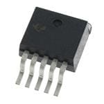
ICGOO电子元器件商城为您提供UCC383TDKTTT-ADJ由Texas Instruments设计生产,在icgoo商城现货销售,并且可以通过原厂、代理商等渠道进行代购。 UCC383TDKTTT-ADJ价格参考¥16.66-¥38.39。Texas InstrumentsUCC383TDKTTT-ADJ封装/规格:PMIC - 稳压器 - 线性, Linear Voltage Regulator IC Positive Adjustable 1 Output 1.22 V ~ 8.5 V 3A DDPAK/TO-263-5。您可以下载UCC383TDKTTT-ADJ参考资料、Datasheet数据手册功能说明书,资料中有UCC383TDKTTT-ADJ 详细功能的应用电路图电压和使用方法及教程。
UCC383TDKTTT-ADJ 是 Texas Instruments(德州仪器)生产的一款线性稳压器,属于 PMIC(电源管理集成电路)中的线性稳压器类别。该器件是一款高精度、可调输出电压的正电压线性稳压器,具有低噪声和快速瞬态响应的特点。

应用场景主要包括:

1. 精密模拟电路供电:适用于需要稳定、低噪声电源的精密运算放大器、模数转换器(ADC)和数模转换器(DAC)等电路。

2. 通信设备:用于无线基站、光模块等通信系统中为敏感射频(RF)和模拟前端提供干净电源。

3. 工业控制系统:如PLC、传感器模块和测量仪器,要求高稳定性和低纹波的电源环境。

4. 测试与测量仪器:如示波器、信号发生器等高精度设备中,确保供电不影响测量精度。

5. 嵌入式系统与DSP/FPGA供电:为数字信号处理器或FPGA的内核或I/O提供稳定电压。

该稳压器采用小型封装,适合空间受限的设计,同时其可调输出特性增强了应用灵活性。
| 参数 | 数值 |
| 产品目录 | 集成电路 (IC)半导体 |
| 描述 | IC REG LDO ADJ 3A DDPAK低压差稳压器 Sgl Output LDO 3.0A Adj Rev Crnt Prot |
| 产品分类 | |
| 品牌 | Texas Instruments |
| 产品手册 | |
| 产品图片 |
|
| rohs | 符合RoHS无铅 / 符合限制有害物质指令(RoHS)规范要求 |
| 产品系列 | 电源管理 IC,低压差稳压器,Texas Instruments UCC383TDKTTT-ADJ- |
| 数据手册 | |
| 产品型号 | UCC383TDKTTT-ADJ |
| 产品种类 | 低压差稳压器 |
| 供应商器件封装 | DDPAK/TO-263-5 |
| 其它名称 | 296-16030-6 |
| 包装 | Digi-Reel® |
| 单位重量 | 1.456 g |
| 商标 | Texas Instruments |
| 回动电压—最大值 | 600 mV at 3 A |
| 安装类型 | 表面贴装 |
| 安装风格 | SMD/SMT |
| 封装 | Reel |
| 封装/外壳 | TO-263-6,D²Pak(5 引线+接片),TO-263BA |
| 封装/箱体 | TO-263-5 |
| 工作温度 | 0°C ~ 70°C |
| 工厂包装数量 | 50 |
| 最大工作温度 | + 70 C |
| 最大输入电压 | 9 V |
| 最小工作温度 | 0 C |
| 最小输入电压 | + 2.8 V |
| 标准包装 | 1 |
| 电压-跌落(典型值) | 0.4V @ 3A |
| 电压-输入 | 2.8 V ~ 9 V |
| 电压-输出 | 1.22 V ~ 8.5 V |
| 电压调节准确度 | 2.5 % |
| 电流-输出 | 3A |
| 电流-限制(最小值) | 4A |
| 稳压器拓扑 | 正,可调式 |
| 稳压器数 | 1 |
| 系列 | UCC383-ADJ |
| 线路调整率 | 3 mV |
| 负载调节 | 5 mV |
| 输入偏压电流—最大 | 0.4 mA |
| 输出电压 | 1.22 V to 8.5 V |
| 输出电流 | 3 A |
| 输出端数量 | 1 Output |
| 输出类型 | Adjustable |


- 商务部:美国ITC正式对集成电路等产品启动337调查
- 曝三星4nm工艺存在良率问题 高通将骁龙8 Gen1或转产台积电
- 太阳诱电将投资9.5亿元在常州建新厂生产MLCC 预计2023年完工
- 英特尔发布欧洲新工厂建设计划 深化IDM 2.0 战略
- 台积电先进制程称霸业界 有大客户加持明年业绩稳了
- 达到5530亿美元!SIA预计今年全球半导体销售额将创下新高
- 英特尔拟将自动驾驶子公司Mobileye上市 估值或超500亿美元
- 三星加码芯片和SET,合并消费电子和移动部门,撤换高东真等 CEO
- 三星电子宣布重大人事变动 还合并消费电子和移动部门
- 海关总署:前11个月进口集成电路产品价值2.52万亿元 增长14.8%


PDF Datasheet 数据手册内容提取
(cid:26) (cid:1)(cid:2)(cid:2)(cid:3)(cid:4)(cid:5)(cid:6)(cid:5)(cid:7) (cid:1)(cid:2)(cid:2)(cid:3)(cid:4)(cid:5)(cid:6)(cid:8)(cid:7) (cid:1)(cid:2)(cid:2)(cid:3)(cid:4)(cid:5)(cid:6)(cid:9)(cid:10)(cid:11)(cid:7) (cid:1)(cid:2)(cid:2)(cid:5)(cid:4)(cid:5)(cid:6)(cid:5)(cid:7) (cid:1)(cid:2)(cid:2)(cid:5)(cid:4)(cid:5)(cid:6)(cid:8)(cid:7) (cid:1)(cid:2)(cid:2)(cid:5)(cid:4)(cid:5)(cid:6)(cid:9)(cid:10)(cid:11) (cid:12)(cid:13)(cid:14)(cid:15)(cid:10)(cid:16)(cid:13)(cid:17)(cid:13)(cid:1)(cid:18) (cid:5)(cid:15)(cid:9) (cid:12)(cid:19)(cid:20)(cid:21)(cid:9)(cid:16) (cid:16)(cid:21)(cid:22)(cid:1)(cid:12)(cid:9)(cid:18)(cid:13)(cid:16) (cid:23)(cid:9)(cid:24)(cid:19)(cid:12)(cid:25) SLUS215B − OCTOBER 1998 − REVISED FEBRUARY 2004 (cid:1) Precision Positive Linear Series Pass TO−263−5 TD PACKAGE TO−263−3 TD PACKAGE (FRONT VIEW) (FRONT VIEW) Voltage Regulation (cid:1) 0.45 V Dropout at 3 A 5 VOUT 4 ADJ 3 VOUT (cid:1) 50 mV Dropout at 10 mA 3 GND 2 GND (cid:1) Quiescent Current Under 650 µA 2 CT 1 VIN 1 VIN Irrespective of Load (cid:1) Adjustable (5-Lead) Output Voltage Version (cid:1) TO−220−5 T PACKAGE Fixed (3-Lead) Versions for 3.3-V and 5-V (FRONT VIEW) Outputs 5 VOUT (cid:1) Logic Shutdown Capability 4 ADJ (cid:1) Short-Circuit Power Limit of + 3 GND 2 CT (3% × V × I ) IN SHORT 1 VIN (cid:1) Low V to V Reverse Leakage OUT IN (cid:1) Thermal Shutdown TO−220−3 T PACKAGE (FRONT VIEW) description 3 VOUT The UCC283−3/−5/−ADJ family of positive linear + 2 GND series pass voltage regulators are tailored for 1 VIN low-drop-out applications where low quiescent power is important. Fabricated with a BiCMOS technology ideally suited for low input-to-output differential applications, the UCC283−5 passes 3 A while requiring only 0.45 V of typical input voltage headroom (ensured 0.6-V dropout). These regulators include reverse voltage sensing that prevents current in the reverse direction. Quiescent current is always less than 650 µA. These devices have been internally compensated in such a way that the need for a minimum output capacitor has been eliminated. UCC283−3 and UCC283−5 versions are in 3-lead packages and have preset outputs at 3.3 V and 5.0 V respectively. The output voltage is regulated to 1.5% at room temperature. The UCC283−ADJ version, in a 5-lead package, regulates the output voltage programmed by an external resistor ratio. Short-circuit current is internally limited. The device responds to a sustained overcurrent condition by turning off after a t time delay. The device then stays off for a period, t , that is 32 times the t delay. The device ON OFF ON then begins pulsing on and off at the t /(t +t ) duty cycle of 3%. This drastically reduces the power ON ON OFF dissipation during short-circuit and means heat sinks need only accommodate normal operation. On the 3-leaded versions of the device t is fixed at 750 µs, on the adjustable 5-leaded versions an external capacitor ON sets the on time. The off time is always 32 × t . The external timing control pin, CT, on the 5-leaded versions ON also serves as a shutdown input when pulled low. Internal power dissipation is further controlled with thermal overload protection circuitry. Thermal shutdown occurs if the junction temperature exceeds 165°C. The chip remains off until the temperature has dropped 20°C. The UCC283 series is specified for operation over the industrial range of −40°C to 85°C, and the UCC383 series is specified from 0°C to 70°C. These devices are available in 3- and 5-pin TO−220 and TO−263 power packages. Please be aware that an important notice concerning availability, standard warranty, and use in critical applications of TexasInstruments semiconductor products and disclaimers thereto appears at the end of this data sheet. All trademarks are the property of their respective owners. (cid:17)(cid:16)(cid:13)(cid:10)(cid:1)(cid:2)(cid:18)(cid:19)(cid:13)(cid:20) (cid:10)(cid:9)(cid:18)(cid:9) (cid:27)(cid:28)(cid:29)(cid:30)(cid:31)!"#(cid:27)(cid:30)(cid:28) (cid:27)$ %&(cid:31)(cid:31)’(cid:28)# "$ (cid:30)(cid:29) (&)*(cid:27)%"#(cid:27)(cid:30)(cid:28) +"#’, Copyright 1998−2004, Texas Instruments Incorporated (cid:17)(cid:31)(cid:30)+&%#$ %(cid:30)(cid:28)(cid:29)(cid:30)(cid:31)! #(cid:30) $(’%(cid:27)(cid:29)(cid:27)%"#(cid:27)(cid:30)(cid:28)$ (’(cid:31) #-’ #’(cid:31)!$ (cid:30)(cid:29) (cid:18)’."$ (cid:19)(cid:28)$#(cid:31)&!’(cid:28)#$ $#"(cid:28)+"(cid:31)+ /"(cid:31)(cid:31)"(cid:28)#0, (cid:17)(cid:31)(cid:30)+&%#(cid:27)(cid:30)(cid:28) ((cid:31)(cid:30)%’$$(cid:27)(cid:28)1 +(cid:30)’$ (cid:28)(cid:30)# (cid:28)’%’$$"(cid:31)(cid:27)*0 (cid:27)(cid:28)%*&+’ #’$#(cid:27)(cid:28)1 (cid:30)(cid:29) "** ("(cid:31)"!’#’(cid:31)$, POST OFFICE BOX 655303 • DALLAS, TEXAS 75265 1
(cid:1)(cid:2)(cid:2)(cid:3)(cid:4)(cid:5)(cid:6)(cid:5)(cid:7) (cid:1)(cid:2)(cid:2)(cid:3)(cid:4)(cid:5)(cid:6)(cid:8)(cid:7) (cid:1)(cid:2)(cid:2)(cid:3)(cid:4)(cid:5)(cid:6)(cid:9)(cid:10)(cid:11)(cid:7) (cid:1)(cid:2)(cid:2)(cid:5)(cid:4)(cid:5)(cid:6)(cid:5)(cid:7) (cid:1)(cid:2)(cid:2)(cid:5)(cid:4)(cid:5)(cid:6)(cid:8)(cid:7) (cid:1)(cid:2)(cid:2)(cid:5)(cid:4)(cid:5)(cid:6)(cid:9)(cid:10)(cid:11) (cid:26) (cid:12)(cid:13)(cid:14)(cid:15)(cid:10)(cid:16)(cid:13)(cid:17)(cid:13)(cid:1)(cid:18) (cid:5)(cid:15)(cid:9) (cid:12)(cid:19)(cid:20)(cid:21)(cid:9)(cid:16) (cid:16)(cid:21)(cid:22)(cid:1)(cid:12)(cid:9)(cid:18)(cid:13)(cid:16) (cid:23)(cid:9)(cid:24)(cid:19)(cid:12)(cid:25) SLUS215B − OCTOBER 1998 − REVISED FEBRUARY 2004 AVAILABLE OPTIONS(1) PACKAGE DEVICES OOUUTTPPUUTT VVOOLLTTAAGGEE ((VV)) TTAA TO−263−3(2) TO−263−5(2) TO−220−3 TO−220−5 MIN TYP MAX TD T 3.22 3.3 3.58 UCC283TD−3 — UCC283T−3 — −−4400°CC ttoo 8855°CC 4.875 5.00 5.125 UCC283TD−5 — UCC283T−5 — ADJ — UCC283TD−ADJ — UCC283T−ADJ 3.22 3.3 3.58 UCC383TD−3 — UCC383T−3 — 00°CC ttoo 7700°CC 4.875 5.00 5.125 UCC383TD−5 — UCC383T−5 — ADJ — UCC383TD−ADJ — UCC383T−ADJ 1. For more package and ordering information, see the Package Option Addendum located at the end of this data sheet. 2. For 50 piece reel, add KTTT (e.g., UCC283TDKTTT−3); for 500 piece reel, add TR (e.g., UCC283TDTR−3). functional block diagram *5 LEADED VERSION ONLY (ADJ) VIN VOUT V PUMP CURRENT LIMIT ADJ* 4 A/ 7 A CURRENT R2 + REFERENCE + 0.65 V 1.25 V R1 3% DUTY CYCLE SD/CT* GND CURRENT LIMIT TIMER REVERSE VOLTAGE R2 R1 SENSE UVLO UCC283−ADJ 0 OPEN THERMAL UCC283−3 82k 50k SHUTDOWN UCC283−5 150k 50k UDG−98133 2 POST OFFICE BOX 655303 • DALLAS, TEXAS 75265
(cid:26) (cid:1)(cid:2)(cid:2)(cid:3)(cid:4)(cid:5)(cid:6)(cid:5)(cid:7) (cid:1)(cid:2)(cid:2)(cid:3)(cid:4)(cid:5)(cid:6)(cid:8)(cid:7) (cid:1)(cid:2)(cid:2)(cid:3)(cid:4)(cid:5)(cid:6)(cid:9)(cid:10)(cid:11)(cid:7) (cid:1)(cid:2)(cid:2)(cid:5)(cid:4)(cid:5)(cid:6)(cid:5)(cid:7) (cid:1)(cid:2)(cid:2)(cid:5)(cid:4)(cid:5)(cid:6)(cid:8)(cid:7) (cid:1)(cid:2)(cid:2)(cid:5)(cid:4)(cid:5)(cid:6)(cid:9)(cid:10)(cid:11) (cid:12)(cid:13)(cid:14)(cid:15)(cid:10)(cid:16)(cid:13)(cid:17)(cid:13)(cid:1)(cid:18) (cid:5)(cid:15)(cid:9) (cid:12)(cid:19)(cid:20)(cid:21)(cid:9)(cid:16) (cid:16)(cid:21)(cid:22)(cid:1)(cid:12)(cid:9)(cid:18)(cid:13)(cid:16) (cid:23)(cid:9)(cid:24)(cid:19)(cid:12)(cid:25) SLUS215B − OCTOBER 1998 − REVISED FEBRUARY 2004 electrical characteristics T = 0°C to 70°C for the UCC383−x series, T = −40°C to 85°C for the A A UCC283−x, V = V + 1.5 V, I = 10 mA, C = 10 (cid:1)F, C = 22 (cid:1)F. For the UCC283−ADJ, V VIN VOUT OUT IN OUT VIN = 6.5 V, VOUT = 5.0 V, CT = 750 pF, TJ = TA unless otherwise stated PARAMETER TEST CONDITIONS MIN TYP MAX UNITS UCC283−5 Fixed 5 V, 3 A Family TJ = 25°C 4.925 5 5.075 V OOuuttppuutt vvoollttaaggee Over temperature 4.875 5.125 V Line regulation VVIN = 5.15 V to 9 V 2 10 mV Load regulation IOUT = 10 mA to 3 A 10 20 mV IOUT = 3 A, VOUT = 4.85 V 0.4 0.6 V DDrrooppoouutt vvoollttaaggee,, VVDDRROOPPOOUUTT == VVVVIINN −− VVVVOOUUTT IOUT = 1.5 A, VOUT = 4.85 V 0.2 0.45 V IOUT = 10 mA, VOUT = 4.85 V 50 150 mV Peak current limit VVOUT = 0 V 4 7 10 A Overcurrent threshold 3 4 5.5 A Current limit duty cycle VVOUT = 0 V 3% 5% Overcurrent time out, tON VVOUT = 0 V 400 750 1400 µs Quiescent current No load 400 650 µA Reverse leakage current 1V VVO <U VTV ≤IN 5 .<1 VVV, aOt UVTV, OUT 30 75 µA Undervoltage lockout VIN where VOUT passes current 2.5 2.8 3 V UCC283−3 Fixed 3.3 V, 3 A Family TJ = 25°C 3.25 3.3 3.35 V OOuuttppuutt vvoollttaaggee Over temperature 3.22 3.38 V Line regulation voltage VVIN = 3.45 V to 9 V 2 7 mV Load regulation voltage IOUT = 10 mA to 3 A 7 15 mV IOUT = 3A, VOUT = 3.15 V 0.5 1 V DDrrooppoouutt vvoollttaaggee,, VVDDRROOPPOOUUTT == VVVVIINN −− VVVVOOUUTT IOUT = 1.5A, VOUT = 3.15 V 0.25 0.6 V IOUT = 10mA, VOUT = 3.15 V 50 150 mV Peak current limit VVOUT = 0 V 4 7 10 A Overcurrent threshold 3 4 5.5 A Current limit duty cycle VVOUT = 0 V 3% 5% Overcurrent time out, tON VVOUT = 0 V 400 750 1400 µs Quiescent current No load 400 650 µA Reverse leakage current 1V VVO <U VTV ≤IN 3 .<3 5V VV OaUt VT,V OUT 30 75 µA Undervoltage lockout VIN where VOUT passes current 2.5 2.8 3 V POST OFFICE BOX 655303 • DALLAS, TEXAS 75265 3
(cid:1)(cid:2)(cid:2)(cid:3)(cid:4)(cid:5)(cid:6)(cid:5)(cid:7) (cid:1)(cid:2)(cid:2)(cid:3)(cid:4)(cid:5)(cid:6)(cid:8)(cid:7) (cid:1)(cid:2)(cid:2)(cid:3)(cid:4)(cid:5)(cid:6)(cid:9)(cid:10)(cid:11)(cid:7) (cid:1)(cid:2)(cid:2)(cid:5)(cid:4)(cid:5)(cid:6)(cid:5)(cid:7) (cid:1)(cid:2)(cid:2)(cid:5)(cid:4)(cid:5)(cid:6)(cid:8)(cid:7) (cid:1)(cid:2)(cid:2)(cid:5)(cid:4)(cid:5)(cid:6)(cid:9)(cid:10)(cid:11) (cid:26) (cid:12)(cid:13)(cid:14)(cid:15)(cid:10)(cid:16)(cid:13)(cid:17)(cid:13)(cid:1)(cid:18) (cid:5)(cid:15)(cid:9) (cid:12)(cid:19)(cid:20)(cid:21)(cid:9)(cid:16) (cid:16)(cid:21)(cid:22)(cid:1)(cid:12)(cid:9)(cid:18)(cid:13)(cid:16) (cid:23)(cid:9)(cid:24)(cid:19)(cid:12)(cid:25) SLUS215B − OCTOBER 1998 − REVISED FEBRUARY 2004 electrical characteristics T = 0°C to 70°C for the UCC383−x series, T = −40°C to 85°C for the A A UCC283−x, V = V + 1.5 V, I = 10 mA, C = 10 (cid:1)F, C = 22 (cid:1)F. For the UCC283−ADJ, V VIN VOUT OUT IN OUT VIN = 6.5 V, VOUT = 5.0 V, CT = 750 pF, TJ = TA unless otherwise stated PARAMETER TEST CONDITIONS MIN TYP MAX UNITS UCC283−ADJ Adjustable Output, 3 A Family TJ = 25°C 1.23 1.25 1.27 V RReegguullaattiinngg vvoollttaaggee aatt AADDJJ ppiinn Over temperature 1.22 1.28 V Line regulation voltage, at ADJ input VVIN = VVOUT + 150 mV to 9 V 1 3 mV Load regulation voltage, at ADJ input IOUT = 10 mA to 3 A 2 5 mV VOUT = 4.85 V, IOUT = 3 A 0.4 0.6 V DDrrooppoouutt vvoollttaaggee,, VVDDRROOPPOOUUTT == VVIINN −− VVOOUUTT VOUT = 4.85 V, IOUT = 1.5 A 0.2 0.45 V VOUT = 4.85 V, IOUT = 10 mA 50 150 mV Peak current limit VVOUT = 0 V 4 7 10 A Overcurrent threshold 3 4 5.5 A Current limit duty cycle VVOUT = 0 V 3 5 % Overcurrent time out, tON VVOUT = 0 V 300 575 1200 µs Reverse leakage current 1V VVO <U VTV ≤IN 9 <V ,V aVt OVUVTOUT 30 100 µA Bias current at ADJ input 20 250 nA Quiescent current No load 400 650 µA Shutdown threshold At CT input 0.25 0.65 V Quiescent current in shutdown VVIN = 9 V 40 75 µA UVLO VIN where VOUT passes current 2.5 2.8 3 V absolute maximum ratings over operating free-air temperature (unless otherwise noted)† Input voltage VIN . . . . . . . . . . . . . . . . . . . . . . . . . . . . . . . . . . . . . . . . . . . . . . . . . . . . . . . . . . . . . . . . . . . . . . . . . . . . . . . . . . . . . 9 V CT . . . . . . . . . . . . . . . . . . . . . . . . . . . . . . . . . . . . . . . . . . . . . . . . . . . . . . . . . . . . . . . . . . . . . . . . . . . . −0.3 V to 3 V ADJ . . . . . . . . . . . . . . . . . . . . . . . . . . . . . . . . . . . . . . . . . . . . . . . . . . . . . . . . . . . . . . . . . . . . . . . . . . . −0.3 V to 9 V Storage Temperature, T . . . . . . . . . . . . . . . . . . . . . . . . . . . . . . . . . . . . . . . . . . . . . . . . . . . . . . . . −65°C to 150°C stg Junction Temperature, T . . . . . . . . . . . . . . . . . . . . . . . . . . . . . . . . . . . . . . . . . . . . . . . . . . . . . . . . . −55°C to 150°C J Lead Temperature (soldering, 10 seconds) . . . . . . . . . . . . . . . . . . . . . . . . . . . . . . . . . . . . . . . . . . . . . . . . . . 300°C †Stresses beyond those listed under “absolute maximum ratings” may cause permanent damage to the device. These are stress ratings only, and functional operation of the device at these or any other conditions beyond those indicated under “recommended operating conditions” is not implied. Exposure to absolute-maximum-rated conditions for extended periods may affect device reliability. 4 POST OFFICE BOX 655303 • DALLAS, TEXAS 75265
(cid:26) (cid:1)(cid:2)(cid:2)(cid:3)(cid:4)(cid:5)(cid:6)(cid:5)(cid:7) (cid:1)(cid:2)(cid:2)(cid:3)(cid:4)(cid:5)(cid:6)(cid:8)(cid:7) (cid:1)(cid:2)(cid:2)(cid:3)(cid:4)(cid:5)(cid:6)(cid:9)(cid:10)(cid:11)(cid:7) (cid:1)(cid:2)(cid:2)(cid:5)(cid:4)(cid:5)(cid:6)(cid:5)(cid:7) (cid:1)(cid:2)(cid:2)(cid:5)(cid:4)(cid:5)(cid:6)(cid:8)(cid:7) (cid:1)(cid:2)(cid:2)(cid:5)(cid:4)(cid:5)(cid:6)(cid:9)(cid:10)(cid:11) (cid:12)(cid:13)(cid:14)(cid:15)(cid:10)(cid:16)(cid:13)(cid:17)(cid:13)(cid:1)(cid:18) (cid:5)(cid:15)(cid:9) (cid:12)(cid:19)(cid:20)(cid:21)(cid:9)(cid:16) (cid:16)(cid:21)(cid:22)(cid:1)(cid:12)(cid:9)(cid:18)(cid:13)(cid:16) (cid:23)(cid:9)(cid:24)(cid:19)(cid:12)(cid:25) SLUS215B − OCTOBER 1998 − REVISED FEBRUARY 2004 pin descriptions ADJ: Adjust pin for the UCC283−ADJ version only. Feedback pin for the linear regulator. Program the output voltage with R1 connected from ADJ to GND and R2 connected from VOUT to ADJ. Output voltage is given by: 1.25V(cid:2)(R1(cid:3)R2) V (cid:1) OUT R1 CT: Short-circuit timing capacitor and shutdown input for the UCC283−ADJ version. Pulling CT below 0.25 V turns off the regulator and places it in a low quiescent-current mode. A timing capacitor, C, from CT to GND programs the duration of the pulsed short-circuit on-time. On-time, t , is approximately given by: ON t (cid:1)750k(cid:2)C ON GND: Reference ground. VIN: Input voltage, This pin must be bypassed with a low ESL/ESR 1-µF or larger capacitor to GND. VIN can range from (VOUT + V ) to 9 V. If VIN is reduced to zero while VOUT is held high, the reverse leakage DROPOUT from VOUT to VIN is less than 75µA. VOUT: Regulated output voltage. A bypass capacitor is not required at VOUT, but may be desired for good transient response. The bypass capacitor must not exceed a maximum value in order to insure the regulator can start. APPLICATION INFORMATION overview The UCC383 family of low dropout linear (LDO) regulators provide a regulated output voltage for applications with up to 3 A of load current. The regulators feature a low dropout voltage and short-circuit protection, making their use ideal for demanding high-current applications requiring fault protection. short-circuit-protection The UCC383 provides unique short-circuit protection circuitry that reduces power dissipation during a fault. When an overload situation is detected, the device enters a pulsed mode of operation at 3% duty cycle reducing the heat sink requirements during a fault. The UCC383 has two current thresholds that determine its behavior during a fault as shown in Figure 1. When the regulator current exceeds the overcurrent threshold for a period longer than t , the UCC383 shuts off for a period (t ) which is 32 × t . During an overload, the regulator ON OFF ON actively limits the maximum current to the peak current limit value. The peak current limit is nominally 3 A greater than the overcurrent threshold. The regulator continues in pulsed mode until the fault is cleared as illustrated in Figure 1. POST OFFICE BOX 655303 • DALLAS, TEXAS 75265 5
(cid:1)(cid:2)(cid:2)(cid:3)(cid:4)(cid:5)(cid:6)(cid:5)(cid:7) (cid:1)(cid:2)(cid:2)(cid:3)(cid:4)(cid:5)(cid:6)(cid:8)(cid:7) (cid:1)(cid:2)(cid:2)(cid:3)(cid:4)(cid:5)(cid:6)(cid:9)(cid:10)(cid:11)(cid:7) (cid:1)(cid:2)(cid:2)(cid:5)(cid:4)(cid:5)(cid:6)(cid:5)(cid:7) (cid:1)(cid:2)(cid:2)(cid:5)(cid:4)(cid:5)(cid:6)(cid:8)(cid:7) (cid:1)(cid:2)(cid:2)(cid:5)(cid:4)(cid:5)(cid:6)(cid:9)(cid:10)(cid:11) (cid:26) (cid:12)(cid:13)(cid:14)(cid:15)(cid:10)(cid:16)(cid:13)(cid:17)(cid:13)(cid:1)(cid:18) (cid:5)(cid:15)(cid:9) (cid:12)(cid:19)(cid:20)(cid:21)(cid:9)(cid:16) (cid:16)(cid:21)(cid:22)(cid:1)(cid:12)(cid:9)(cid:18)(cid:13)(cid:16) (cid:23)(cid:9)(cid:24)(cid:19)(cid:12)(cid:25) SLUS215B − OCTOBER 1998 − REVISED FEBRUARY 2004 APPLICATION INFORMATION PEAK OVERLOAD CURRENT OUTPUT LIMIT CURRENT OVER− CURRENT THRESHOLD IO (NOM) VO (NOM) ROL ICL OUTPUT VOLTAGE TON 32 TON TON 32 TON TON 32 TON Figure 1. UCC383 Short-Circuit Timing A capacitive load on the regulator’s output appears as a short-circuit during start-up. If the capacitance is too large, the output voltage does not come into regulation during the initial t period and the UCC383 enters ON pulsed mode operation. The peak current limit, t period, and load characteristics determine the maximum ON value of output capacitor that can be charged. For a constant current load the maximum output capacitance is given as follows: (cid:4) (cid:6) t C (cid:1) I (cid:5)I (cid:2) ON Farads OUT(max) CL LOAD V OUT (1) For worst case calculations, the minimum values of on time (t ) and peak current limit (I ) should be used. ON CL The adjustable version allows the t time to be adjusted with a capacitor on the CT pin: ON t (cid:1)750,000(cid:2)C((cid:1)Farad)microseconds ON(adj) (2) For a resistive load (R ) the maximum output capacitor can be estimated from: LOAD t ON(sec) C (cid:1) Farads OUT(max) (cid:9) (cid:11) (cid:8) (cid:8) R (cid:2)(cid:7)n 1 LOAD (cid:10)1(cid:5) VOUT (cid:12) I (cid:2)R CL LOAD (3) 6 POST OFFICE BOX 655303 • DALLAS, TEXAS 75265
(cid:26) (cid:1)(cid:2)(cid:2)(cid:3)(cid:4)(cid:5)(cid:6)(cid:5)(cid:7) (cid:1)(cid:2)(cid:2)(cid:3)(cid:4)(cid:5)(cid:6)(cid:8)(cid:7) (cid:1)(cid:2)(cid:2)(cid:3)(cid:4)(cid:5)(cid:6)(cid:9)(cid:10)(cid:11)(cid:7) (cid:1)(cid:2)(cid:2)(cid:5)(cid:4)(cid:5)(cid:6)(cid:5)(cid:7) (cid:1)(cid:2)(cid:2)(cid:5)(cid:4)(cid:5)(cid:6)(cid:8)(cid:7) (cid:1)(cid:2)(cid:2)(cid:5)(cid:4)(cid:5)(cid:6)(cid:9)(cid:10)(cid:11) (cid:12)(cid:13)(cid:14)(cid:15)(cid:10)(cid:16)(cid:13)(cid:17)(cid:13)(cid:1)(cid:18) (cid:5)(cid:15)(cid:9) (cid:12)(cid:19)(cid:20)(cid:21)(cid:9)(cid:16) (cid:16)(cid:21)(cid:22)(cid:1)(cid:12)(cid:9)(cid:18)(cid:13)(cid:16) (cid:23)(cid:9)(cid:24)(cid:19)(cid:12)(cid:25) SLUS215B − OCTOBER 1998 − REVISED FEBRUARY 2004 APPLICATION INFORMATION dropout performance Referring to the Block Diagram, the dropout voltage of the UCC383 is equal to the minimum voltage drop (V IN to V ) across the N-channel MOSFET. The dropout voltage is dependent on operating conditions such as OUT load current, input and load voltages, as well as temperature. The UCC383 achieves a low Rds(on) through the use of an internal charge-pump (V ) that drives the MOSFET gate. Figure 2 depicts typical dropout voltages PUMP versus load current for the 3.3-V and 5-V versions of the part, as well as the adjustable version programmed to 3.0 V. Figure 3 depicts the typical dropout performance of the adjustable version with various output voltages and load currents. Operating temperatures also affect the Rds(on) and dropout voltage of the UCC383. Figure 4 graphs the typical dropout for the 3.3-V and 5-V versions with a 3-A load over temperature. TYPICAL DROPOUT VOLTAGE TYPICAL DROPOUT VOLTAGE vs. vs. LOAD CURRENT IOUT AND VOUT 0.5 0.8 VOUT = 3.3 V 0.7 0.4 0.6 (V)UT0.3 VOUT = 3 V (V)UT0.5 IOUT = 3 A V−VINO0.2 VOUT = 5 V V−VINO00..34 IOUT = 1.5 A 0.1 0.2 0.1 I = 1 A 0 OUT 0 1 1.5 2 2.5 3 3 3.5 4 4.5 5 IOUT (A) VOUT (V) Figure 2 Figure 3 POST OFFICE BOX 655303 • DALLAS, TEXAS 75265 7
(cid:1)(cid:2)(cid:2)(cid:3)(cid:4)(cid:5)(cid:6)(cid:5)(cid:7) (cid:1)(cid:2)(cid:2)(cid:3)(cid:4)(cid:5)(cid:6)(cid:8)(cid:7) (cid:1)(cid:2)(cid:2)(cid:3)(cid:4)(cid:5)(cid:6)(cid:9)(cid:10)(cid:11)(cid:7) (cid:1)(cid:2)(cid:2)(cid:5)(cid:4)(cid:5)(cid:6)(cid:5)(cid:7) (cid:1)(cid:2)(cid:2)(cid:5)(cid:4)(cid:5)(cid:6)(cid:8)(cid:7) (cid:1)(cid:2)(cid:2)(cid:5)(cid:4)(cid:5)(cid:6)(cid:9)(cid:10)(cid:11) (cid:26) (cid:12)(cid:13)(cid:14)(cid:15)(cid:10)(cid:16)(cid:13)(cid:17)(cid:13)(cid:1)(cid:18) (cid:5)(cid:15)(cid:9) (cid:12)(cid:19)(cid:20)(cid:21)(cid:9)(cid:16) (cid:16)(cid:21)(cid:22)(cid:1)(cid:12)(cid:9)(cid:18)(cid:13)(cid:16) (cid:23)(cid:9)(cid:24)(cid:19)(cid:12)(cid:25) SLUS215B − OCTOBER 1998 − REVISED FEBRUARY 2004 APPLICATION INFORMATION voltage programming and shutdown feature for adjustable version A typical application circuit based on the UCC383 adjustable version is shown in Figure 5. The output voltage is externally programmed through a resistive divider at the ADJ pin. TYPICAL DROPOUT VOLTAGE vs. CASE TEMPERATURE WITH A 3-A LOAD 0.6 V) 0.5 VOUT = 3.3 V (T U O V 0.4 − N V = 5 V VI OUT 0.3 0.2 −40 10 60 Temperature ((cid:1)C) Figure 4 (cid:4) (cid:6) V (cid:1)1.25(cid:2) 1(cid:3)R2 Volts OUT R1 (4) The maximum programmed output voltage is constrained by the 9-V absolute rating of the IC (this includes the charge pump voltage) and its ability to enhance the N-channel MOSFET. Unless the load current is below the 3-A rating of the device, output voltages above 7 V are not recommended. The minimum output voltage can be programmed down to 1.25 V. However, the input voltage must always be greater than the UVLO of the part. The adjustable version includes a shutdown feature, limiting quiescent current to 40 µA typical. The UCC383 is shut down by pulling the CT pin to below 0.25 V. As shown in Figure 5, a small logic level MOSFET or BJT transistor in parallel with the timing capacitor can be driven with a digital signal, putting the device in shutdown. If the CT pin is not pulled low, the IC internally pulls up the pin enabling the regulator. The CT pin should not be forced high, as this interferes with the short-circuit-protection feature. Selection of the timing capacitor is explained in Short-Circuit-Protection. The adjustable version can be used in applications requiring remote voltage sensing (i.e. monitoring a voltage other than or not directly tied to the VOUT pin). This is possible since the inverting input of the error-voltage amplifier (see Block Diagram) is brought out to the ADJ pin. 8 POST OFFICE BOX 655303 • DALLAS, TEXAS 75265
(cid:26) (cid:1)(cid:2)(cid:2)(cid:3)(cid:4)(cid:5)(cid:6)(cid:5)(cid:7) (cid:1)(cid:2)(cid:2)(cid:3)(cid:4)(cid:5)(cid:6)(cid:8)(cid:7) (cid:1)(cid:2)(cid:2)(cid:3)(cid:4)(cid:5)(cid:6)(cid:9)(cid:10)(cid:11)(cid:7) (cid:1)(cid:2)(cid:2)(cid:5)(cid:4)(cid:5)(cid:6)(cid:5)(cid:7) (cid:1)(cid:2)(cid:2)(cid:5)(cid:4)(cid:5)(cid:6)(cid:8)(cid:7) (cid:1)(cid:2)(cid:2)(cid:5)(cid:4)(cid:5)(cid:6)(cid:9)(cid:10)(cid:11) (cid:12)(cid:13)(cid:14)(cid:15)(cid:10)(cid:16)(cid:13)(cid:17)(cid:13)(cid:1)(cid:18) (cid:5)(cid:15)(cid:9) (cid:12)(cid:19)(cid:20)(cid:21)(cid:9)(cid:16) (cid:16)(cid:21)(cid:22)(cid:1)(cid:12)(cid:9)(cid:18)(cid:13)(cid:16) (cid:23)(cid:9)(cid:24)(cid:19)(cid:12)(cid:25) SLUS215B − OCTOBER 1998 − REVISED FEBRUARY 2004 APPLICATION INFORMATION thermal design The Package Information section of the Power Supply Control Products Data Book, Volume 3 (Literature No. SLUD003) contains reference material for the thermal ratings of various packages. The section also includes an excellent article Thermal Characteristics of Surface Mount Packages, that is the basis of the following discussion. Thermal design for the UCC383 family of linear regulators includes two modes of operation, normal and pulsed mode. In normal operation, the linear regulator and heat sink must dissipate power equal to the maximum forward voltage drop multiplied by the maximum load current. Assuming a constant current load, the expected heat rise at the regulator’s junction can be calculated as follows: (cid:4) (cid:6) t ((cid:2))(cid:1)P (cid:2) (cid:2) (cid:3)(cid:2) °C RISE DISS jc ca (5) Where theta, (θ) is thermal resistance and P is the power dissipated. The thermal resistance of both the DISS TO−220 and TO−263 packages (junction to case) is 3°C per Watt. In order to prevent the regulator from going into thermal shutdown, the case to ambient theta must keep the junction temperature below 150°C. If the LDO is mounted on a 5-square inch pad of 1-ounce copper, for example, the thermal resistance from junction to ambient becomes 60°C per Watt. If a lower thermal resistance is required by the application, the device heat sinking would need to be improved. When the UCC383 regulator is in pulsed mode due to an overload or short-circuit in the application, the maximum average power dissipation is calculated as follows: (cid:4) (cid:6) t P (cid:1) V (cid:5)V (cid:2)I (cid:2) ON Watts PULSE(avg) IN OUT CL 33(cid:2)t ON (6) As seen in Equation 6, the average power during a fault is reduced dramatically by the duty cycle, allowing the heat sink to be sized for normal operation. Although the peak power in the regulator during the t period can ON be significant, the thermal mass of the package generally keeps the junction temperature from rising unless the t period is increased to tens of milliseconds. ON ripple rejection Even though the UCC383 family of linear regulators are not optimized for fast transient applications (Refer to the UC182 Fast LDO Linear Regulator), they do offer significant power supply rejection at lower frequencies. Figure 6 depicts ripple rejection performance in a typical application. The performance can be improved with additional filtering. POST OFFICE BOX 655303 • DALLAS, TEXAS 75265 9
(cid:1)(cid:2)(cid:2)(cid:3)(cid:4)(cid:5)(cid:6)(cid:5)(cid:7) (cid:1)(cid:2)(cid:2)(cid:3)(cid:4)(cid:5)(cid:6)(cid:8)(cid:7) (cid:1)(cid:2)(cid:2)(cid:3)(cid:4)(cid:5)(cid:6)(cid:9)(cid:10)(cid:11)(cid:7) (cid:1)(cid:2)(cid:2)(cid:5)(cid:4)(cid:5)(cid:6)(cid:5)(cid:7) (cid:1)(cid:2)(cid:2)(cid:5)(cid:4)(cid:5)(cid:6)(cid:8)(cid:7) (cid:1)(cid:2)(cid:2)(cid:5)(cid:4)(cid:5)(cid:6)(cid:9)(cid:10)(cid:11) (cid:26) (cid:12)(cid:13)(cid:14)(cid:15)(cid:10)(cid:16)(cid:13)(cid:17)(cid:13)(cid:1)(cid:18) (cid:5)(cid:15)(cid:9) (cid:12)(cid:19)(cid:20)(cid:21)(cid:9)(cid:16) (cid:16)(cid:21)(cid:22)(cid:1)(cid:12)(cid:9)(cid:18)(cid:13)(cid:16) (cid:23)(cid:9)(cid:24)(cid:19)(cid:12)(cid:25) SLUS215B − OCTOBER 1998 − REVISED FEBRUARY 2004 APPLICATION INFORMATION UCC383−ADJ V 1 VIN VOUT 5 INPUT 10µF 10µF R LOAD R2 2 CT ADJ 4 SHUTDOWN R1 GND 3 Figure 5. Typical Application for 5-Pin Adjustable Version Figure 6. Ripple Rejection vs. Frequency 10 POST OFFICE BOX 655303 • DALLAS, TEXAS 75265
PACKAGE OPTION ADDENDUM www.ti.com 6-Feb-2020 PACKAGING INFORMATION Orderable Device Status Package Type Package Pins Package Eco Plan Lead/Ball Finish MSL Peak Temp Op Temp (°C) Device Marking Samples (1) Drawing Qty (2) (6) (3) (4/5) UCC283T-ADJ ACTIVE TO-220 KC 5 50 Green (RoHS Call TI | SN N / A for Pkg Type UCC283T-ADJ & no Sb/Br) UCC283TDKTTT-5 ACTIVE DDPAK/ KTT 3 50 Green (RoHS Call TI | SN Level-2-260C-1 YEAR -40 to 85 UCC283TD-5 TO-263 & no Sb/Br) UCC283TDTR-3 ACTIVE DDPAK/ KTT 3 500 Green (RoHS Call TI | SN Level-2-260C-1 YEAR UCC283TD-3 TO-263 & no Sb/Br) UCC283TDTR-ADJ ACTIVE DDPAK/ KTT 5 500 Green (RoHS Call TI | SN Level-2-260C-1 YEAR -40 to 85 UCC283TD-ADJ TO-263 & no Sb/Br) UCC383T-ADJ ACTIVE TO-220 KC 5 50 Green (RoHS Call TI | SN N / A for Pkg Type UCC383T-ADJ & no Sb/Br) UCC383TDKTTT-5 ACTIVE DDPAK/ KTT 3 50 Green (RoHS Call TI | SN Level-2-260C-1 YEAR 0 to 70 UCC383TD-5 TO-263 & no Sb/Br) UCC383TDTR-3 ACTIVE DDPAK/ KTT 3 500 Green (RoHS Call TI | SN Level-2-260C-1 YEAR UCC383TD-3 TO-263 & no Sb/Br) UCC383TDTR-ADJ ACTIVE DDPAK/ KTT 5 500 Green (RoHS Call TI | SN Level-2-260C-1 YEAR UCC383TD-ADJ TO-263 & no Sb/Br) UCC383TDTR-ADJG3 ACTIVE DDPAK/ KTT 5 500 Green (RoHS SN Level-2-260C-1 YEAR 0 to 70 UCC383TD-ADJ TO-263 & no Sb/Br) (1) The marketing status values are defined as follows: ACTIVE: Product device recommended for new designs. LIFEBUY: TI has announced that the device will be discontinued, and a lifetime-buy period is in effect. NRND: Not recommended for new designs. Device is in production to support existing customers, but TI does not recommend using this part in a new design. PREVIEW: Device has been announced but is not in production. Samples may or may not be available. OBSOLETE: TI has discontinued the production of the device. (2) RoHS: TI defines "RoHS" to mean semiconductor products that are compliant with the current EU RoHS requirements for all 10 RoHS substances, including the requirement that RoHS substance do not exceed 0.1% by weight in homogeneous materials. Where designed to be soldered at high temperatures, "RoHS" products are suitable for use in specified lead-free processes. TI may reference these types of products as "Pb-Free". RoHS Exempt: TI defines "RoHS Exempt" to mean products that contain lead but are compliant with EU RoHS pursuant to a specific EU RoHS exemption. Green: TI defines "Green" to mean the content of Chlorine (Cl) and Bromine (Br) based flame retardants meet JS709B low halogen requirements of <=1000ppm threshold. Antimony trioxide based flame retardants must also meet the <=1000ppm threshold requirement. (3) MSL, Peak Temp. - The Moisture Sensitivity Level rating according to the JEDEC industry standard classifications, and peak solder temperature. Addendum-Page 1
PACKAGE OPTION ADDENDUM www.ti.com 6-Feb-2020 (4) There may be additional marking, which relates to the logo, the lot trace code information, or the environmental category on the device. (5) Multiple Device Markings will be inside parentheses. Only one Device Marking contained in parentheses and separated by a "~" will appear on a device. If a line is indented then it is a continuation of the previous line and the two combined represent the entire Device Marking for that device. (6) Lead/Ball Finish - Orderable Devices may have multiple material finish options. Finish options are separated by a vertical ruled line. Lead/Ball Finish values may wrap to two lines if the finish value exceeds the maximum column width. Important Information and Disclaimer:The information provided on this page represents TI's knowledge and belief as of the date that it is provided. TI bases its knowledge and belief on information provided by third parties, and makes no representation or warranty as to the accuracy of such information. Efforts are underway to better integrate information from third parties. TI has taken and continues to take reasonable steps to provide representative and accurate information but may not have conducted destructive testing or chemical analysis on incoming materials and chemicals. TI and TI suppliers consider certain information to be proprietary, and thus CAS numbers and other limited information may not be available for release. In no event shall TI's liability arising out of such information exceed the total purchase price of the TI part(s) at issue in this document sold by TI to Customer on an annual basis. Addendum-Page 2
PACKAGE MATERIALS INFORMATION www.ti.com 19-May-2020 TAPE AND REEL INFORMATION *Alldimensionsarenominal Device Package Package Pins SPQ Reel Reel A0 B0 K0 P1 W Pin1 Type Drawing Diameter Width (mm) (mm) (mm) (mm) (mm) Quadrant (mm) W1(mm) UCC283TDTR-3 DDPAK/ KTT 3 500 330.0 24.4 10.6 15.6 4.9 16.0 24.0 Q2 TO-263 UCC283TDTR-ADJ DDPAK/ KTT 5 500 330.0 24.4 10.6 15.6 4.9 16.0 24.0 Q2 TO-263 UCC383TDTR-3 DDPAK/ KTT 3 500 330.0 24.4 10.6 15.6 4.9 16.0 24.0 Q2 TO-263 UCC383TDTR-ADJ DDPAK/ KTT 5 500 330.0 24.4 10.6 15.6 4.9 16.0 24.0 Q2 TO-263 PackMaterials-Page1
PACKAGE MATERIALS INFORMATION www.ti.com 19-May-2020 *Alldimensionsarenominal Device PackageType PackageDrawing Pins SPQ Length(mm) Width(mm) Height(mm) UCC283TDTR-3 DDPAK/TO-263 KTT 3 500 367.0 367.0 45.0 UCC283TDTR-ADJ DDPAK/TO-263 KTT 5 500 367.0 367.0 45.0 UCC383TDTR-3 DDPAK/TO-263 KTT 3 500 367.0 367.0 45.0 UCC383TDTR-ADJ DDPAK/TO-263 KTT 5 500 367.0 367.0 45.0 PackMaterials-Page2
None
None
PACKAGE OUTLINE KC0005A TO-220 - 16.51 mm max height SCALE 0.850 TO-220 4.83 B 4.06 10.67 1.40 AAAAA 8.89 3.05 9.65 1.14 6.86 2.54 6.86 (6.275) 5.69 3.71-3.96 OPTIONAL 12.88 CHAMFER 10.08 16.51 2X (R1) MAX OPTIONAL 9.25 7.67 (4.25) C PIN 1 ID (OPTIONAL) NOTE 3 14.73 12.29 1 5 0.61 1.02 5X 0.30 0.64 3.05 0.25 C A B 2.03 4X 1.7 6.8 1 5 4215009/A 01/2017 NOTES: 1. All controlling linear dimensions are in inches. Dimensions in brackets are in millimeters. Any dimension in brackets or parenthesis are for reference only. Dimensioning and tolerancing per ASME Y14.5M. 2. This drawing is subject to change without notice. 3. Shape may vary per different assembly sites. www.ti.com
EXAMPLE BOARD LAYOUT KC0005A TO-220 - 16.51 mm max height TO-220 4X (1.45) PKG 0.07 MAX METAL 0.07 MAX ALL AROUND (1.45) TYP ALL AROUND PKG (2) 4X (2) 1 5 (R0.05) TYP SOLDER MASK FULL R (1.7) TYP OPENING, TYP TYP 5X ( 1.2) (6.8) LAND PATTERN NON-SOLDER MASK DEFINED SCALE:12X 4215009/A 01/2017 www.ti.com
None
None
IMPORTANTNOTICEANDDISCLAIMER TI PROVIDES TECHNICAL AND RELIABILITY DATA (INCLUDING DATASHEETS), DESIGN RESOURCES (INCLUDING REFERENCE DESIGNS), APPLICATION OR OTHER DESIGN ADVICE, WEB TOOLS, SAFETY INFORMATION, AND OTHER RESOURCES “AS IS” AND WITH ALL FAULTS, AND DISCLAIMS ALL WARRANTIES, EXPRESS AND IMPLIED, INCLUDING WITHOUT LIMITATION ANY IMPLIED WARRANTIES OF MERCHANTABILITY, FITNESS FOR A PARTICULAR PURPOSE OR NON-INFRINGEMENT OF THIRD PARTY INTELLECTUAL PROPERTY RIGHTS. These resources are intended for skilled developers designing with TI products. You are solely responsible for (1) selecting the appropriate TI products for your application, (2) designing, validating and testing your application, and (3) ensuring your application meets applicable standards, and any other safety, security, or other requirements. These resources are subject to change without notice. TI grants you permission to use these resources only for development of an application that uses the TI products described in the resource. Other reproduction and display of these resources is prohibited. No license is granted to any other TI intellectual property right or to any third party intellectual property right. TI disclaims responsibility for, and you will fully indemnify TI and its representatives against, any claims, damages, costs, losses, and liabilities arising out of your use of these resources. TI’s products are provided subject to TI’s Terms of Sale (www.ti.com/legal/termsofsale.html) or other applicable terms available either on ti.com or provided in conjunction with such TI products. TI’s provision of these resources does not expand or otherwise alter TI’s applicable warranties or warranty disclaimers for TI products. Mailing Address: Texas Instruments, Post Office Box 655303, Dallas, Texas 75265 Copyright © 2020, Texas Instruments Incorporated