ICGOO在线商城 > 集成电路(IC) > PMIC - 稳压器 - 线性 > TPS79928DDCR
 Datasheet下载
- 型号: TPS79928DDCR
- 制造商: Texas Instruments
- 库位|库存: xxxx|xxxx
- 要求:
| 数量阶梯 | 香港交货 | 国内含税 |
| +xxxx | $xxxx | ¥xxxx |
查看当月历史价格
查看今年历史价格
TPS79928DDCR产品简介:
ICGOO电子元器件商城为您提供TPS79928DDCR由Texas Instruments设计生产,在icgoo商城现货销售,并且可以通过原厂、代理商等渠道进行代购。 TPS79928DDCR价格参考。Texas InstrumentsTPS79928DDCR封装/规格:PMIC - 稳压器 - 线性, Linear Voltage Regulator IC Positive Fixed 1 Output 2.8V 200mA SOT-23-5。您可以下载TPS79928DDCR参考资料、Datasheet数据手册功能说明书,资料中有TPS79928DDCR 详细功能的应用电路图电压和使用方法及教程。
TPS79928DDCR 是 Texas Instruments(德州仪器)推出的一款低功耗、低压降 (LDO) 线性稳压器,属于 PMIC - 稳压器 - 线性分类。该器件具有以下特点和应用场景:

 特点:
1. 低静态电流:TPS79928 的静态电流非常低,仅为 150 nA(典型值),非常适合电池供电设备以延长续航时间。
2. 宽输入电压范围:支持 1.6 V 至 6.5 V 的输入电压范围,能够适应多种电源环境。
3. 固定输出电压:TPS79928DDCR 提供固定的 2.8 V 输出电压,适用于对电压稳定性要求较高的场景。
4. 高精度输出:输出电压精度高达 ±1%,确保系统运行的可靠性。
5. 快速启动时间:启动时间短,能够快速响应负载变化。
6. 小型封装:采用 DDC 封装(WSON-6,1.5 mm × 1.5 mm),适合空间受限的设计。

 应用场景:
1. 便携式电子设备:
   - 如智能手机、平板电脑、可穿戴设备等需要低功耗和小尺寸设计的产品。
   - 在这些设备中,TPS79928 可为 MCU、传感器、RF 模块等提供稳定的电源供应。

2. 物联网 (IoT) 设备:
   - 用于低功耗无线传感器节点、智能家庭设备等。
   - 其超低静态电流特性使得它非常适合长时间待机或休眠模式下的应用。

3. 电池供电系统:
   - 包括遥控器、电子标签、便携式医疗设备等。
   - 能够高效管理电池能量,延长设备使用寿命。

4. 工业控制:
   - 在工业自动化领域,可用于为微控制器、通信接口电路等提供稳定电源。
   - 其宽输入电压范围和高精度输出使其适应复杂的工业环境。

5. 消费类电子产品:
   - 如蓝牙耳机、智能家居控制器等。
   - TPS79928 的小尺寸和低功耗特性使其成为这些产品的理想选择。

总之,TPS79928DDCR 凭借其低功耗、高精度和小型化设计,广泛应用于对能效和空间有严格要求的各种电子设备中。
| 参数 | 数值 |
| 产品目录 | 集成电路 (IC)半导体 |
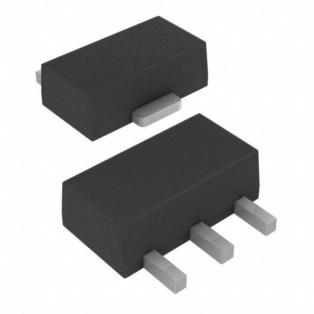
| 描述 | IC REG LDO 2.8V 0.2A 5SOT低压差稳压器 200mA High PSRR LDO |
| 产品分类 | |
| 品牌 | Texas Instruments |
| 产品手册 | |
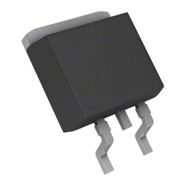
| 产品图片 |
|
| rohs | 符合RoHS无铅 / 符合限制有害物质指令(RoHS)规范要求 |
| 产品系列 | 电源管理 IC,低压差稳压器,Texas Instruments TPS79928DDCR- |
| 数据手册 | |
| 产品型号 | TPS79928DDCR |
| PCN组件/产地 | |
| 产品目录页面 | |
| 产品种类 | 低压差稳压器 |
| 供应商器件封装 | 5-SOT |
| 其它名称 | 296-17781-1 |
| 包装 | 剪切带 (CT) |
| 商标 | Texas Instruments |
| 回动电压—最大值 | 175 mV at 200 mA |
| 安装类型 | 表面贴装 |
| 安装风格 | SMD/SMT |
| 封装 | Reel |
| 封装/外壳 | SOT-23-5 细型,TSOT-23-5 |
| 封装/箱体 | SOT-23-5 |
| 工作温度 | -40°C ~ 125°C |
| 工厂包装数量 | 3000 |
| 最大功率耗散 | 0.5 W |
| 最大工作温度 | + 125 C |
| 最大输入电压 | 6.5 V |
| 最小工作温度 | - 40 C |
| 最小输入电压 | + 2.7 V |
| 标准包装 | 1 |
| 电压-跌落(典型值) | 0.1V @ 200mA |
| 电压-输入 | 最高 6.5V |
| 电压-输出 | 2.8V |
| 电压调节准确度 | 1 % |
| 电流-输出 | 200mA |
| 电流-限制(最小值) | 200mA |
| 稳压器拓扑 | 正,固定式 |
| 稳压器数 | 1 |
| 系列 | TPS79928 |
| 线路调整率 | 0.02 % / V |
| 负载调节 | 0.002 % / mA |
| 输入偏压电流—最大 | 0.04 mA |
| 输出电压 | 2.8 V |
| 输出电流 | 200 mA |
| 输出端数量 | 1 Output |
| 输出类型 | Fixed |
| 配用 | /product-detail/zh/TPS799XXEVM-105/296-21172-ND/1216778 |


- 商务部:美国ITC正式对集成电路等产品启动337调查
- 曝三星4nm工艺存在良率问题 高通将骁龙8 Gen1或转产台积电
- 太阳诱电将投资9.5亿元在常州建新厂生产MLCC 预计2023年完工
- 英特尔发布欧洲新工厂建设计划 深化IDM 2.0 战略
- 台积电先进制程称霸业界 有大客户加持明年业绩稳了
- 达到5530亿美元!SIA预计今年全球半导体销售额将创下新高
- 英特尔拟将自动驾驶子公司Mobileye上市 估值或超500亿美元
- 三星加码芯片和SET,合并消费电子和移动部门,撤换高东真等 CEO
- 三星电子宣布重大人事变动 还合并消费电子和移动部门
- 海关总署:前11个月进口集成电路产品价值2.52万亿元 增长14.8%


PDF Datasheet 数据手册内容提取
Product Sample & Technical Tools & Support & Folder Buy Documents Software Community TPS799 SBVS056K–JANUARY2005–REVISEDJANUARY2015 TPS799 200-mA, Low-Quiescent Current, Ultralow Noise, High-PSRR Low-Dropout Linear Regulator 1 Features 3 Description • 200-mALow-DropoutRegulatorWithEN The TPS799 family of low-dropout (LDO), low-power 1 linear regulators offers excellent ac performance with • MultipleOutputVoltageVersionsAvailable: very low ground current. High power-supply rejection – FixedOutputsof1.2Vto4.5VUsing ratio (PSRR), low noise, fast start-up, and excellent InnovativeFactoryEEPROMProgramming line and load transient response are provided while – AdjustableOutputsfrom1.20Vto6.5V consumingaverylow40-μA(typical)groundcurrent. • InrushCurrentProtectionwithENToggle The TPS799 is stable with ceramic capacitors and uses an advanced BiCMOS fabrication process to • LowI :40μA Q yield a dropout voltage of typically 100 mV at a • HighPSRR:66dBat1kHz 200-mA output. The TPS799 uses a precision voltage • StablewithaLow-ESR,2-μFTypicalOutput reference and feedback loop to achieve an overall Capacitance accuracy of 2% over all load, line, process, and temperature variations. The TPS799 features inrush • ExcellentLoadandLineTransientResponse current protection when the EN toggle is used to start • 2%OverallAccuracy(Load,Line,and thedevice,immediatelyclampingthecurrent. Temperature) All devices are fully specified over the temperature • VeryLowDropout:100mV range of T = –40°C to 125°C, and offered in a low- J • Package:5-Bump,Thin,1-mm× 1.37-mm profile, die-sized ball grid array (DSBGA) package, DSBGA idealforwirelesshandsetsandWLANcards. 2 Applications DeviceInformation(1) • CellularPhones PARTNUMBER PACKAGE BODYSIZE(NOM) • WirelessLAN,Bluetooth® SOT(5) 2.90mmx1.60mm TPS799 SON(6) 2.00x2.00mm • VCOs,RF DSBGA(5) 1.57mmx1.20mm • HandheldOrganizers,PDAs (1) For all available packages, see the orderable addendum at theendofthedatasheet. TypicalApplicationCircuit TypicalApplicationCircuit FixedVoltageVersions AdjustableVoltageVersion Optionalinputcapacitor. Optional input capacitor. (R + R) Mayimprovesource May improve source VOUT= 1R 2 ´1.193 impedance,noise,orPSRR. impedance, noise, or PSRR. 2 VIN IN OUT VOUT VIN IN OUT VOUT TPS799xx TPS79901 R C 1 FB 2.2mF 2.2mF EN GND NR Ceramic EN GND FB Ceramic R 2 V EN Optionalbypasscapacitor VEN toreduceoutputnoise andincreasePSRR. 1 An IMPORTANT NOTICE at the end of this data sheet addresses availability, warranty, changes, use in safety-critical applications, intellectualpropertymattersandotherimportantdisclaimers.PRODUCTIONDATA.
TPS799 SBVS056K–JANUARY2005–REVISEDJANUARY2015 www.ti.com Table of Contents 1 Features.................................................................. 1 7.4 DeviceFunctionalModes........................................13 2 Applications........................................................... 1 8 ApplicationandImplementation........................ 14 3 Description............................................................. 1 8.1 ApplicationInformation............................................14 4 RevisionHistory..................................................... 2 8.2 TypicalApplications................................................14 8.3 Do'sandDon'ts ......................................................16 5 PinConfigurationandFunctions......................... 3 9 PowerSupplyRecommendations...................... 16 5.1 FixedVoltageVersions.............................................3 5.2 AdjustableVoltageVersions.....................................3 10 Layout................................................................... 16 6 Specifications......................................................... 5 10.1 LayoutGuidelines.................................................16 6.1 AbsoluteMaximumRatings......................................5 10.2 LayoutExample....................................................17 6.2 ESDRatings ............................................................5 10.3 ThermalInformation..............................................17 6.3 RecommendedOperatingConditions.......................5 11 DeviceandDocumentationSupport................. 18 6.4 ThermalInformation..................................................5 11.1 DeviceSupport......................................................18 6.5 ElectricalCharacteristics...........................................6 11.2 DocumentationSupport........................................18 6.6 TypicalCharacteristics..............................................7 11.3 Trademarks...........................................................18 7 DetailedDescription............................................ 12 11.4 ElectrostaticDischargeCaution............................18 7.1 Overview.................................................................12 11.5 Glossary................................................................18 7.2 FunctionalBlockDiagram.......................................12 12 Mechanical,Packaging,andOrderable Information........................................................... 18 7.3 FeatureDescription.................................................13 4 Revision History NOTE:Pagenumbersforpreviousrevisionsmaydifferfrompagenumbersinthecurrentversion. ChangesfromRevisionJ(August2010)toRevisionK Page • AddedESDRatingstable,FeatureDescriptionsection,DeviceFunctionalModes,ApplicationandImplementation section,PowerSupplyRecommendationssection,Layoutsection,DeviceandDocumentationSupportsection,and Mechanical,Packaging,andOrderableInformationsection ................................................................................................. 1 • ChangedFeatureslist ........................................................................................................................................................... 1 • ChangedDescriptionsection.................................................................................................................................................. 1 • Changedfigureonfrontpage;replaceddevicepinoutswithapplicationcircuits................................................................... 1 • ChangedPinConfigurationandFunctionssection;updatedtableformat,renamedpinpackagestomeetnew standards ............................................................................................................................................................................... 3 • Changed"free-air"to"junction"temperatureinconditionstatementforAbsoluteMaximumRatings .................................. 5 • Changedfree-airtojunctioninRecommendedOperatingConditionstableconditions......................................................... 5 • Addedthermalinformationforadditionaldevicepackages ................................................................................................... 5 ChangesfromRevisionI(November2007)toRevisionJ Page • ReplacedtheDissipationRatingstablewiththeThermalInformationtable.......................................................................... 5 2 SubmitDocumentationFeedback Copyright©2005–2015,TexasInstrumentsIncorporated ProductFolderLinks:TPS799
TPS799 www.ti.com SBVS056K–JANUARY2005–REVISEDJANUARY2015 5 Pin Configuration and Functions 5.1 Fixed Voltage Versions DDCPackage 5-PinSOT YZUPackage TopView 5-PinDSBGA TopView C3 C1 IN 1 5 OUT IN OUT GND 2 B2 GND EN 3 4 NR A3 A1 NR EN DRVPackage 6-PinSONWithExposedThermalPad TopView OUT 1 6 IN NR 2 GND 5 N/C GND 3 4 EN 5.2 Adjustable Voltage Versions DDCPackage 5-PinSOT YZUPackage TopView 5-PinDSBGA TopView C3 C1 IN 1 5 OUT IN OUT GND 2 B2 GND EN 3 4 FB A3 A1 FB EN DRVPackage 6-PinSONWithExposedThermalPad TopView OUT 1 6 IN FB 2 GND 5 N/C GND 3 4 EN Copyright©2005–2015,TexasInstrumentsIncorporated SubmitDocumentationFeedback 3 ProductFolderLinks:TPS799
TPS799 SBVS056K–JANUARY2005–REVISEDJANUARY2015 www.ti.com PinFunctions PIN I/O DESCRIPTION NAME DDC YZY DRV IN 1 C3 6 I Inputsupply. GND 2 B2 3,Pad — Ground.ThepadmustbetiedtoGND. Drivingthispinhighturnsontheregulator.Drivingthispinlowputstheregulatorinto EN 3 A1 4 I shutdownmode.ENcanbeconnectedtoINifnotused. Fixedvoltageversionsonly.Noisereduction;connectingthispintoanexternalcapacitor NR 4 A3 2 — bypassesnoisegeneratedbytheinternalbandgap.Thiscapacitorallowsoutputnoiseto bereducedtoverylowlevels. Adjustablevoltageversiononly.Feedback;thispinistheinputtothecontrollooperror FB 4 A3 2 I amplifier,andsetstheoutputvoltageofthedevice. Outputoftheregulator.Toassurestability,asmallceramiccapacitor(totaltypical OUT 5 C1 1 O capacitance≥2μF)isrequiredfromthispintoground. N/C — — 5 — Notinternallyconnected.Thispinmusteitherbeleftopen,ortiedtoGND. 4 SubmitDocumentationFeedback Copyright©2005–2015,TexasInstrumentsIncorporated ProductFolderLinks:TPS799
TPS799 www.ti.com SBVS056K–JANUARY2005–REVISEDJANUARY2015 6 Specifications 6.1 Absolute Maximum Ratings overoperatingjunctiontemperaturerange(unlessotherwisenoted) (1) MIN MAX UNIT IN –0.3 7.0 V Voltage(2) EN –0.3 V +0.3 V IN OUT –0.3 V +0.3 V IN Current OUT Internallylimited mA Operatingvirtualjunction,T –55 150 °C J Temperature Storagetemperaturerange,T –55 150 °C stg (1) StressesbeyondthoselistedunderAbsoluteMaximumRatingsmaycausepermanentdamagetothedevice.Thesearestressratings only,whichdonotimplyfunctionaloperationofthedeviceattheseoranyotherconditionsbeyondthoseindicatedunderRecommended OperatingConditions.Exposuretoabsolute-maximum-ratedconditionsforextendedperiodsmayaffectdevicereliability. (2) Allvoltagesarewithrespecttonetworkgroundterminal. 6.2 ESD Ratings VALUE UNIT Humanbodymodel(HBM),perANSI/ESDA/JEDECJS-001,allpins(1) ±2000 Electrostatic V(ESD) discharge Calhlapringse(d2)devicemodel(CDM),perJEDECspecificationJESD22-C101, ±500 V (1) JEDECdocumentJEP155statesthat500-VHBMallowssafemanufacturingwithastandardESDcontrolprocess. (2) JEDECdocumentJEP157statesthat250-VCDMallowssafemanufacturingwithastandardESDcontrolprocess. 6.3 Recommended Operating Conditions overoperatingjunctiontemperaturerange(unlessotherwisenoted) MIN NOM MAX UNIT V Inputvoltage 2.7 6.5 V IN I Outputcurrent 0.5 200 mA OUT T Operatingjunctiontemperature –40 125 °C J 6.4 Thermal Information TPS799 THERMALMETRIC(1) DDC(SOT) DRV(SON) YZU(DSBGA) UNIT 5PINS 6PINS 5PINS R Junction-to-ambientthermalresistance 225.3 74.2 143.3 θJA R Junction-to-case(top)thermalresistance 39.3 58.8 1.1 θJC(top) R Junction-to-boardthermalresistance 47.3 145.9 84.7 θJB °C/W ψ Junction-to-topcharacterizationparameter 0.5 0.2 3.8 JT ψ Junction-to-boardcharacterizationparameter 46.7 54.4 84.4 JB R Junction-to-case(bottom)thermalresistance N/A 7.2 N/A θJC(bot) (1) Formoreinformationabouttraditionalandnewthermalmetrics,seetheICPackageThermalMetricsapplicationreport,SPRA953. Copyright©2005–2015,TexasInstrumentsIncorporated SubmitDocumentationFeedback 5 ProductFolderLinks:TPS799
TPS799 SBVS056K–JANUARY2005–REVISEDJANUARY2015 www.ti.com 6.5 Electrical Characteristics Overoperatingtemperaturerange(T =–40°Cto125°C),V =V +0.3Vor2.7V,whicheverisgreater;I =1mA, J IN OUT(nom) OUT V =V ,C =2.2μF,C =0.01μF,unlessotherwisenoted.ForTPS79901,V =3.0V.TypicalvaluesareatT = EN IN OUT NR OUT J 25°C. PARAMETER TESTCONDITIONS MIN TYP MAX UNIT V Inputvoltagerange(1) 2.7 6.5 V IN V Internalreference(TPS79901) 1.169 1.193 1.217 V FB V Outputvoltagerange(TPS79901) V 6.5–V V OUT FB DO Outputaccuracy,nominal T =25°C –1% 1% J VOUT Outputaccuracy(1) VOUT+0.3V≤VIN≤6.5V –2% ±1% 2% OverV ,I ,temperature 500μA≤I ≤200mA IN OUT OUT ΔV Lineregulation(1) V +0.3V≤V ≤6.5V 0.02 %/V O(ΔVI) OUT(NOM) IN ΔV Loadregulation 500μA≤I ≤200mA 0.002 %/mA O(ΔIO) OUT Dropoutvoltage(2) VOUT(nom)≤3.3V 100 175 mV V I =200mA DO (VIN=VOUT(nom)–0.1V) OUT VOUT(nom)≥3.3V 90 160 mV I Outputcurrentlimit V =0.9×V 220 400 600 mA CL OUT OUT(nom) I Groundpincurrent 500μA≤I ≤200mA 40 60 μA GND OUT I Shutdowncurrent(I ) V ≤0.4V,2.7V≤V ≤6.5V 0.15 1 μA SHDN GND EN IN I Feedbackpincurrent(TPS79901) –0.5 0.5 µA FB f=100Hz 70 dB V =3.85V, IN V =2.85V, f=1kHz 66 dB PSRR Power-supplyrejectionratio OUT CNR=0.01μF, f=10kHz 51 dB I =100mA OUT f=100kHz 38 dB BW=10Hzto100kHz, CNR=0.01μF 10.5×VOUT μVRMS V Outputnoisevoltage n VOUT=2.85V CNR=none 94×VOUT μVRMS C =0.001μF 45 μs NR VOUT=2.85V, CNR=0.047μF 45 μs Start-uptime R =14Ω, L COUT=2.2μF CNR=0.01μF 50 μs C =none 50 μs NR V Enablehigh(enabled) 1.2 V V EN(HI) IN V Enablelow(shutdown) 0 0.4 V EN(LO) I Enablepincurrent,enabled V =V =6.5V 0.03 1 μA EN(HI) EN IN Shutdown,temperatureincreasing 165 °C T Thermalshutdowntemperature sd Reset,temperaturedecreasing 145 °C T Operatingjunctiontemperature –40 125 °C J Undervoltagelockout V rising 1.90 2.20 2.65 V IN UVLO Hysteresis V falling 70 mV IN (1) MinimumV =V +V or2.7V,whicheverisgreater. IN OUT DO (2) V isnotmeasuredfordeviceswithV <2.8VbecauseminimumV =2.7V. DO OUT(nom) IN 6 SubmitDocumentationFeedback Copyright©2005–2015,TexasInstrumentsIncorporated ProductFolderLinks:TPS799
TPS799 www.ti.com SBVS056K–JANUARY2005–REVISEDJANUARY2015 6.6 Typical Characteristics Overoperatingtemperaturerange(T=–40°Cto125°C),V =V +0.3Vor2.7V,whicheverisgreater;I =1mA, J IN OUT(nom) OUT V =V ,C =2.2μF,andC =0.01μF,unlessotherwisenoted.ForTPS79901,V =3.0V.TypicalvaluesareatT EN IN OUT NR OUT J =25°C. 28.50 1.0 I =100mA 0.8 OUT 21.38 0.6 V(mV)OUT 147..21530 TJ = +25°C TJ = −40°C nV(%)OUT 00..420 TJ = −40°C TJ = +25°C Changein -- -12741...123358 TJ = +125°C TJ = +85°C Changei ---- 0000....2468 TJ = +85°C TJ = +125°C - 28.50 - 1.0 0 50 100 150 200 2.5 3.5 4.5 5.5 6.5 7.5 IOUT(mA) VIN(V) Figure1.LoadRegulation Figure2.LineRegulation 2.0 200 1.5 180 T =+125(cid:1)C J 160 1.0 (%) IOUT=1mA I =100mA 140 TJ=+85(cid:1)C OUT 0.5 OUT V) 120 V m n 0 ( 100 i O nge - 0.5 VD 80 T =+25(cid:1)C Cha - 1.0 IOUT=200mA 60 J 40 - 1.5 20 TJ=- 40(cid:1)C - 2.0 0 - 40 - 25 - 15 5 20 35 50 65 80 95 110 125 0 50 100 150 200 TJ (°C) IOUT(mA) Figure3.OutputVoltagevsJunctionTemperature Figure4.TPS799285DropoutVoltagevsOutputCurrent 200 110 I =200mA 180 100 OUT 160 90 I =200mA OUT 80 140 70 mV) 120 mV) 60 V(DO 10800 IOUT=100mA V(DO 5400 60 30 40 20 20 10 I =1mA OUT 0 0 - 40 - 25 - 15 5 20 35 50 65 80 95 110 125 2.5 3.0 3.5 4.0 4.5 5.0 5.5 6.0 6.5 7.0 TJ (°C) VIN(V) Figure5.TPS799285DropoutVoltagevsJunction Figure6.TPS79901DropoutvsInputVoltage Temperature Copyright©2005–2015,TexasInstrumentsIncorporated SubmitDocumentationFeedback 7 ProductFolderLinks:TPS799
TPS799 SBVS056K–JANUARY2005–REVISEDJANUARY2015 www.ti.com Typical Characteristics (continued) Overoperatingtemperaturerange(T=–40°Cto125°C),V =V +0.3Vor2.7V,whicheverisgreater;I =1mA, J IN OUT(nom) OUT V =V ,C =2.2μF,andC =0.01μF,unlessotherwisenoted.ForTPS79901,V =3.0V.TypicalvaluesareatT EN IN OUT NR OUT J =25°C. 60 60 V =3.2V IN 50 50 V =5.0V I = 200mA IN OUT 40 40 A) IOUT= 500mA A) m ( 30 m( 30 GND GND VIN=2.7V I I (dropout) 20 20 10 10 V =2.85V VOUT= 2.85V IOOUUTT=200mA 0 0 2.5 3.0 3.5 4.0 4.5 5.0 5.5 6.0 6.5 7.0 - 40 - 25 - 15 5 20 35 50 65 80 95 110 125 VIN(V) TJ (°C) Figure7.GroundPinCurrentvsInputVoltage Figure8.TPS799285GroundPinCurrentvsJunction Temperature 600 90 VEN=0.4V 80 IOUT=100mA 500 I =1mA 70 OUT 400 60 (nA)ND 300 RR(dB) 5400 IOUT=200mA G S I P 200 30 V =6.5V IN 20 100 C =0.01m F VIN=3.2V 10 CNORUT=2.2m F 0 0 - 40 - 25 - 15 5 20 35 50 65 80 95 110 125 10 100 1k 10k 100k 1M 10M TJ (°C) Frequency(Hz) Figure9.GroundPinCurrent(Disabled)vsJunction Figure10.TPS799285Power-SupplyRippleRejectionvs Temperature Frequency(VIN–VOUT=1.0V) 90 90 80 IOUT=100mA IOUT=1mA 80 I =1mA OUT 70 70 60 60 B) B) d 50 d 50 RR( 40 RR( 40 IOUT=200mA S S P P 30 30 20 20 10 CCNR==02.0.21mm FF IOUT=200mA 10 CCNR==02.0.21mm FF IOUT=100mA OUT OUT 0 0 10 100 1k 10k 100k 1M 10M 10 100 1k 10k 100k 1M 10M Frequency(Hz) Frequency(Hz) Figure11.TPS799285Power-SupplyRippleRejectionvs Figure12.TPS799285Power-SupplyRippleRejectionvs Frequency(V –V =0.5V) Frequency(V –V =0.25V) IN OUT IN OUT 8 SubmitDocumentationFeedback Copyright©2005–2015,TexasInstrumentsIncorporated ProductFolderLinks:TPS799
TPS799 www.ti.com SBVS056K–JANUARY2005–REVISEDJANUARY2015 Typical Characteristics (continued) Overoperatingtemperaturerange(T=–40°Cto125°C),V =V +0.3Vor2.7V,whicheverisgreater;I =1mA, J IN OUT(nom) OUT V =V ,C =2.2μF,andC =0.01μF,unlessotherwisenoted.ForTPS79901,V =3.0V.TypicalvaluesareatT EN IN OUT NR OUT J =25°C. 90 90 80 80 IOUT=1mA IOUT=1mA 70 70 60 60 B) IOUT=200mA B) d 50 d 50 ( ( R R R 40 R 40 PS PS IOUT=200mA 30 30 20 20 10 CCNORUT==01.001.0m mFF 10 CCNORUT==01.001.0m mFF 0 0 10 100 1k 10k 100k 1M 10M 10 100 1k 10k 100k 1M 10M Frequency(Hz) Frequency(Hz) Figure13.TPS799285Power-SupplyRippleRejectionvs Figure14.TPS799285Power-SupplyRippleRejectionvs Frequency(VIN–VOUT=1.0V) Frequency(VIN–VOUT=0.25V) 90 90 1MHz 0.1kHz 1kHz 80 80 70 70 I =1mA OUT 60 60 B) B) (d 50 (d 50 R R R 40 R 40 PS PS 10kHz 100kHz 30 30 20 20 10 CCNR==N1o0n.e0m F IOUT=200mA 10 CCNR==02.0.21mm FF OUT OUT 0 0 10 100 1k 10k 100k 1M 10M 0.0 0.5 1.0 1.5 2.0 2.5 3.0 3.5 4.0 Frequency(Hz) V - V (V) IN OUT Figure15.TPS799285Power-SupplyRippleRejectionvs Figure16.Power-SupplyRippleRejectionvsV –V ,I IN OUT OUT Frequency(VIN–VOUT=1.0V) =1mA 90 90 0.1kHz 0.1kHz 80 80 1kHz 1kHz 70 70 60 60 B) 10kHz B) 10kHz d 50 d 50 ( ( R R R 40 R 40 S S P P 30 30 100kHz 1MHz 1MHz 100kHz 20 20 C =0.01m F C =0.01m F 10 CNR =2.2m F 10 CNR =2.2m F OUT OUT 0 0 0.0 0.5 1.0 1.5 2.0 2.5 3.0 3.5 4.0 0.0 0.5 1.0 1.5 2.0 2.5 3.0 3.5 4.0 V - V (V) V - V (V) IN OUT IN OUT Figure17.Power-SupplyRippleRejectionvsV –V ,I Figure18.Power-SupplyRippleRejectionvsV –V ,I IN OUT OUT IN OUT OUT =100mA =200mA Copyright©2005–2015,TexasInstrumentsIncorporated SubmitDocumentationFeedback 9 ProductFolderLinks:TPS799
TPS799 SBVS056K–JANUARY2005–REVISEDJANUARY2015 www.ti.com Typical Characteristics (continued) Overoperatingtemperaturerange(T=–40°Cto125°C),V =V +0.3Vor2.7V,whicheverisgreater;I =1mA, J IN OUT(nom) OUT V =V ,C =2.2μF,andC =0.01μF,unlessotherwisenoted.ForTPS79901,V =3.0V.TypicalvaluesareatT EN IN OUT NR OUT J =25°C. 200 35 I =1mA 180 COOUUTT=2.2m F 30 160 ms) 140 ms) 25 Vr 120 Vr 20 mNoise( 10800 mNoise( 15 Total 60 Total 10 40 5 I =1mA 20 COUT=0.01m F NR 0 0 0.01 0.1 1 10 0 5 10 15 20 25 CNR(nF) COUT(m F) Figure19.TPS799285TotalNoisevsC Figure20.TPS799285TotalNoisevsC NR OUT IOUT=150mA VIN= 3.35V COUT= 2.2mF 100mV/div V C =10m F OUT OUT 20mV/div V OUT COUT= 10mF 100mV/div VOUT C =2.2m F OUT 20mV/div VOUT 150mA dV 4.15V IN =1V/m s dt 100mA/div 1mA 3.15V IOUT 1V/div V IN 20m s/div 20ms/div Figure21.TPS799285LineTransientResponse Figure22.TPS799285LoadTransientResponse RCLOOUATD== 2 1.29mWF VOUT CROLUOTAD= =2 .129mWF RLOAD= V19INW= 3.85V VOUT COUT= 10mF RLOAD= 19W COUT= 10mF 1V/div 1V/div 3.85V V V 0V IN EN 4V/div 5V/div 10ms/div 10ms/div Figure23.TPS799285Turn-OnResponse(V =V ) Figure24.TPS799285EnableResponse EN IN 10 SubmitDocumentationFeedback Copyright©2005–2015,TexasInstrumentsIncorporated ProductFolderLinks:TPS799
TPS799 www.ti.com SBVS056K–JANUARY2005–REVISEDJANUARY2015 Typical Characteristics (continued) Overoperatingtemperaturerange(T=–40°Cto125°C),V =V +0.3Vor2.7V,whicheverisgreater;I =1mA, J IN OUT(nom) OUT V =V ,C =2.2μF,andC =0.01μF,unlessotherwisenoted.ForTPS79901,V =3.0V.TypicalvaluesareatT EN IN OUT NR OUT J =25°C. 7 R =19W L 6 V IN 5 4 s olt 3 V V OUT 2 1 0 - 1 50ms/div Figure25.TPS799285Power-Up/Power-Down Copyright©2005–2015,TexasInstrumentsIncorporated SubmitDocumentationFeedback 11 ProductFolderLinks:TPS799
TPS799 SBVS056K–JANUARY2005–REVISEDJANUARY2015 www.ti.com 7 Detailed Description 7.1 Overview The TPS799 family of low-dropout (LDO) regulators combines the high performance required of many RF and precision analog applications with ultralow current consumption. High PSRR is provided by a high-gain, high- bandwidth error loop with good supply rejection at very low headroom (V – V ). A noise-reduction pin is IN OUT provided to bypass noise generated by the band-gap reference and to improve PSRR, while a quick-start circuit quickly charges this capacitor at start-up. The combination of high performance and low ground current also make these devices an excellent choice for portable applications. All versions have thermal and overcurrent protection,andarefullyspecifiedfrom–40°Cto125°C. The TPS799 family also features inrush current protection with an EN toggle start-up, and overshoot detection at the output. When the EN toggle is used to start the device, current limit protection is immediately activated, restricting the inrush current to the device. If voltage at the output overshoots 5% from the nominal value, a pulldownresistorreducesthevoltagetonormaloperatingconditions,asshownintheFunctionalBlockDiagram. 7.2 Functional Block Diagram IN OUT 400W 2m A Current Limit EN Thermal Overshoot Shutdown Detect UVLO Quickstart 1.193V NR Bandgap 500k GND Figure26. Fixed-VoltageVersions 12 SubmitDocumentationFeedback Copyright©2005–2015,TexasInstrumentsIncorporated ProductFolderLinks:TPS799
TPS799 www.ti.com SBVS056K–JANUARY2005–REVISEDJANUARY2015 Functional Block Diagram (continued) IN OUT 400W 3.3MW Current Limit EN Thermal Overshoot Shutdown Detect UVLO 1.193V FB Bandgap 500k GND Figure27. Adjustable-VoltageVersions 7.3 Feature Description 7.3.1 InternalCurrentLimit The TPS799 internal current limit helps protect the regulator during fault conditions. In current limit mode, the output sources a fixed amount of current that is largely independent of the output voltage. For reliable operation, donotoperatethedeviceinacurrent-limitstateforextendedperiodsoftime. ThePMOSpasselementintheTPS799hasabuilt-inbodydiodethatconductscurrentwhenthevoltageatOUT exceeds the voltage at IN. This current is not limited; therefore, if extended reverse voltage operation is anticipated,externallimitingmayberequired. 7.3.2 Shutdown The enable pin (EN) is active high and is compatible with standard and low-voltage TTL-CMOS levels. When shutdowncapabilityisnotrequired,ENcanbeconnectedtoIN. 7.3.3 StartUp The TPS799 uses a start-up circuit to quickly charge the noise reduction capacitor, C , if present (see the NR Functional Block Diagram). This circuit allows for the combination of very low output noise and fast start-up times. The NR pin is high impedance so a low leakage C capacitor must be used; most ceramic capacitors are NR appropriateforthisconfiguration. Notethatforfasteststart-up,applyV first,andthendrivetheenablepin(EN)high.IfENistiedtoIN,start-upis IN somewhat slower. The start-up switch is closed for approximately 135 μs. To ensure that C is fully charged NR duringstart-up,usea0.01-μForsmallercapacitor. 7.3.4 UndervoltageLockout(UVLO) The TPS799 uses an undervoltage lockout circuit to keep the output shut off until internal circuitry is operating properly. The UVLO circuit has a deglitch feature so that undershoot transients are typically ignored on the input ifthesetransientsarelessthan50 μsinduration. 7.4 Device Functional Modes Driving EN over 1.2 V turns on the regulator. Driving EN below 0.4 V puts the regulator into shutdown mode, thusreducingtheoperatingcurrentto150nA,nominal. Copyright©2005–2015,TexasInstrumentsIncorporated SubmitDocumentationFeedback 13 ProductFolderLinks:TPS799
TPS799 SBVS056K–JANUARY2005–REVISEDJANUARY2015 www.ti.com 8 Application and Implementation NOTE Information in the following applications sections is not part of the TI component specification, and TI does not warrant its accuracy or completeness. TI’s customers are responsible for determining suitability of components for their purposes. Customers should validateandtesttheirdesignimplementationtoconfirmsystemfunctionality. 8.1 Application Information The TPS799 family of LDO regulators provides high PSRR while maintaining ultralow current consumption. The familyalsofeaturesinrushcurrentprotectionandovershootdetectionattheoutput. 8.2 Typical Applications Figure28andFigure29showthebasiccircuitconnections. Optionalinputcapacitor. Mayimprovesource impedance,noise,orPSRR. VIN IN OUT VOUT TPS799xx 2.2mF EN GND NR Ceramic V EN Optionalbypasscapacitor toreduceoutputnoise andincreasePSRR. Figure28. TypicalApplicationCircuitforFixedVoltageVersions Optional input capacitor. (R + R) May improve source VOUT= 1R 2 ´1.193 impedance, noise, or PSRR. 2 VIN IN OUT VOUT TPS79901 R C 1 FB 2.2mF EN GND FB Ceramic R 2 V EN Figure29. TypicalApplicationCircuitforAdjustableVoltageVersion 8.2.1 DesignRequirements Selectthedesireddevicebasedontheoutputvoltage. Provide an input supply with adequate headroom to account for dropout and output current to account for the GNDterminalcurrent,andpowertheload. 8.2.2 DetailedDesignProcedure 8.2.2.1 InputandOutputCapacitorRequirements Although an input capacitor is not required for stability, good analog design practice is to connect a 0.1-μF to 1-μF low ESR capacitor across the input supply near the regulator. This capacitor counteracts reactive input sources and improves transient response, noise rejection, and ripple rejection. A higher-value capacitor may be necessaryiflarge,fastrise-timeloadtransientsareanticipated,orifthedeviceislocatedseveralinchesfromthe power source. If source impedance is not sufficiently low, a 0.1-μF input capacitor may be necessary to ensure stability. 14 SubmitDocumentationFeedback Copyright©2005–2015,TexasInstrumentsIncorporated ProductFolderLinks:TPS799
TPS799 www.ti.com SBVS056K–JANUARY2005–REVISEDJANUARY2015 Typical Applications (continued) The TPS799 is designed to be stable with standard ceramic capacitors with values of 2.2 μF or greater. X5R- and X7R-type capacitors are best because they have minimal variation in value and ESR over temperature. MaximumESRmustbelessthan1.0 Ω. 8.2.2.2 OutputNoise In most LDOs, the band gap is the dominant noise source. If a noise-reduction capacitor (C ) is used with the NR TPS799, the band gap does not contribute significantly to noise. Instead, noise is dominated by the output resistor divider and the error amplifier input. To minimize noise in a given application, use a 0.01-μF noise reduction capacitor. To further optimize noise, equivalent series resistance of the output capacitor can be set to approximately 0.2 Ω. This configuration maximizes phase margin in the control loop, reducing total output noise byupto10%. Noisecanbereferredtothefeedbackpoint;withC =0.01 μFtotalnoiseisapproximatelygivenbyEquation1: NR 10.5mV V = R M S x V N V OUT (1) 8.2.2.3 DropoutVoltage The TPS799 uses a PMOS pass transistor to achieve a low dropout voltage. When (V – V ) is less than the IN OUT dropout voltage (V ), the PMOS pass device is in its linear region of operation and r of the PMOS pass DO DS(on) element is the input-to-output resistance. Because the PMOS device behaves like a resistor in dropout, V DO approximatelyscaleswiththeoutputcurrent. As with any linear regulator, PSRR degrades as (V – V ) approaches dropout. This effect is illustrated in IN OUT Figure10throughFigure18 intheTypicalCharacteristicssection. 8.2.2.4 TransientResponse As with any regulator, increasing the size of the output capacitor reduces over- and undershoot magnitude, but increasesthedurationofthetransientresponse.ThetransientresponseoftheTPS799isenhancedbyanactive pulldown device that engages when the output overshoots by approximately 5% or more when the device is enabled.Whenenabled,thepulldowndevicebehaveslikea350-Ω resistortoground. 8.2.2.5 MinimumLoad The TPS799 is stable with no output load. To meet the specified accuracy, a minimum load of 500 μA is required. With loads less than 500 μA at junction temperatures near 125°C, the output can drift up enough to cause the output pulldown device to turn on. The output pulldown device limits voltage drift to 5% typically; however, ground current can increase by approximately 50 μA. In typical applications, the junction cannot reach high temperatures at light loads because there is no noticeable dissipated power. The specified ground current is thenvalidatnoloadinmostapplications. 8.2.2.6 FeedbackCapacitorRequirements(TPS79901Only) The feedback capacitor, C , shown in Figure 29 is required for stability. For a parallel combination of R and R FB 1 2 equal to 250 kΩ, any value from 3 pF to 1 nF can be used. Fixed voltage versions have an internal 30-pF feedback capacitor which is quick-charged at start-up. The adjustable version does not have this quick-charge circuit, so values below 5 pF should be used to ensure fast startup; values above 47 pF can be used to implement an output voltage soft-start. Larger value capacitors also improve noise slightly. The TPS79901 is stableinunity-gainconfiguration(OUTtiedtoFB)withoutC . FB Copyright©2005–2015,TexasInstrumentsIncorporated SubmitDocumentationFeedback 15 ProductFolderLinks:TPS799
TPS799 SBVS056K–JANUARY2005–REVISEDJANUARY2015 www.ti.com Typical Applications (continued) 8.2.3 ApplicationCurve 100 90 IOUT = 1 mA IOUT = 100 mA 80 IOUT = 250 mA 70 B) 60 d R ( 50 R S 40 P 30 20 10 COUT = 2.2 µF CNR = 0.01 µF 0 10 100 1k 10k 100k 1M 10M Frequency (Hz) G001 Figure30.Power-SupplyRejectionRatiovsFrequency 8.3 Do's and Don'ts Doplaceatleastone2.2-µFceramiccapacitorascloseaspossibletotheOUTpinoftheregulator. Donotplacetheoutputcapacitormorethan10mmawayfromtheregulator. Do connect a 0.1-μF to 1-μF low equivalent series resistance (ESR) capacitor across the IN pin and GND input oftheregulator. Donotexceedtheabsolutemaximumratings. 9 Power Supply Recommendations These devices are designed to operate from an input voltage supply range between 2.7 V and 6.5 V. The input voltage range provides adequate headroom in order for the device to have a regulated output. This input supply is well-regulated and stable. If the input supply is noisy, additional input capacitors with low ESR can help improvetheoutputnoiseperformance. 10 Layout 10.1 Layout Guidelines 10.1.1 BoardLayoutRecommendationstoImprovePSRRandNoisePerformance To improve ac performance (such as PSRR, output noise, and transient response), design the board with separate ground planes for V and V , with each ground plane connected only at the GND pin of the device. IN OUT Inaddition,connectthebypasscapacitordirectlytotheGNDpinofthedevice. 16 SubmitDocumentationFeedback Copyright©2005–2015,TexasInstrumentsIncorporated ProductFolderLinks:TPS799
TPS799 www.ti.com SBVS056K–JANUARY2005–REVISEDJANUARY2015 10.2 Layout Example VI VO TPS799 CIN COUT EN GND CNR Represents via used for application specific connections. Figure31. LayoutExample 10.3 Thermal Information 10.3.1 ThermalProtection Thermal protection disables the output when the junction temperature rises to approximately 165°C, allowing the devicetocool.Whenthejunctiontemperaturecoolstoapproximately145°Ctheoutputcircuitryisagainenabled. Depending on power dissipation, thermal resistance, and ambient temperature, the thermal protection circuit may cycle on and off. This cycling limits the dissipation of the regulator, protecting it from damage resulting from overheating. Any tendency to activate the thermal protection circuit indicates excessive power dissipation or an inadequate heatsink. For reliable operation, limit junction temperature to 125°C maximum. To estimate the margin of safety in a complete design (including heatsink), increase the ambient temperature until the thermal protection is triggered; use worst-case loads and signal conditions. For good reliability, thermal protection triggers at least 35°C above the maximum expected ambient condition of a particular application. This configuration produces a worst-casejunctiontemperatureof125°Catthehighestexpectedambienttemperatureandworst-caseload. The internal protection circuitry of the TPS799 is designed to protect against overload conditions. This circuitry is not intended to replace proper heatsinking. Continuously running the device into thermal shutdown degrades devicereliability. 10.3.2 PowerDissipation The ability to remove heat from the die is different for each package type, presenting different considerations in the PCB layout. The PCB area around the device that is free of other components moves the head from the device to the ambient air. Performance data for JEDEC low- and high-K boards are given in the Thermal Information table near the front of this data sheet. Using heavier copper increases the effectiveness in removing heat from the device. The addition of plated through-holes to heat-dissipating layers also improves heatsink effectiveness. Power dissipation depends on input voltage and load conditions. Power dissipation is equal to the product of the outputcurrenttimesthevoltagedropacrosstheoutputpasselement,asshowninEquation2: PD(cid:2)(cid:4)VIN(cid:1)VOUT(cid:5)(cid:3)IOUT (2) 10.3.3 PackageMounting SolderpadfootprintrecommendationsfortheTPS799areavailablefromtheTI'swebsiteatwww.ti.com. Copyright©2005–2015,TexasInstrumentsIncorporated SubmitDocumentationFeedback 17 ProductFolderLinks:TPS799
TPS799 SBVS056K–JANUARY2005–REVISEDJANUARY2015 www.ti.com 11 Device and Documentation Support 11.1 Device Support 11.1.1 DevelopmentSupport 11.1.1.1 EvaluationModules An evaluation module (EVM) is available to assist in the initial circuit performance evaluation using the TPS799. This EVM, the TPS799 evaluation module, can be requested at the Texas Instruments web site through the productfoldersorpurchaseddirectlyfromtheTIeStore. 11.1.1.2 SpiceModels Computer simulation of circuit performance using SPICE is often useful when analyzing the performance of analog circuits and systems. A SPICE model for the TPS799 is available through the product folders under simulationmodels. 11.1.2 DeviceNomenclature Table1. DeviceNomenclature(1) PRODUCT V OUT TPS799xx(x)yyyz xx(x)isnominaloutputvoltage(forexample,28=2.8V,285=2.85V,01=Adjustable). yyyispackagedesignator. zispackagequantity. (1) ForthemostcurrentpackageandorderinginformationseethePackageOptionAddendumattheendofthisdocument,orvisitthe deviceproductfolderatwww.ti.com. 11.2 Documentation Support 11.2.1 RelatedDocumentation Forrelateddocumentation,seethefollowing: • Applicationreport: UsingNewThermalMetrics,SBVA025. • Applicationreport: ICPackageThermalMetrics,SPRA953 • TPS799xxEVM-105User'sGuide,SLVU130 11.3 Trademarks BluetoothisaregisteredtrademarkofBluetoothSIG,Inc. Allothertrademarksarethepropertyoftheirrespectiveowners. 11.4 Electrostatic Discharge Caution This integrated circuit can be damaged by ESD. Texas Instruments recommends that all integrated circuits be handled with appropriateprecautions.Failuretoobserveproperhandlingandinstallationprocedurescancausedamage. ESDdamagecanrangefromsubtleperformancedegradationtocompletedevicefailure.Precisionintegratedcircuitsmaybemore susceptibletodamagebecauseverysmallparametricchangescouldcausethedevicenottomeetitspublishedspecifications. 11.5 Glossary SLYZ022—TIGlossary. Thisglossarylistsandexplainsterms,acronyms,anddefinitions. 12 Mechanical, Packaging, and Orderable Information The following pages include mechanical, packaging, and orderable information. This information is the most current data available for the designated devices. This data is subject to change without notice and revision of thisdocument.Forbrowser-basedversionsofthisdatasheet,refertotheleft-handnavigation. 18 SubmitDocumentationFeedback Copyright©2005–2015,TexasInstrumentsIncorporated ProductFolderLinks:TPS799
PACKAGE OPTION ADDENDUM www.ti.com 6-Feb-2020 PACKAGING INFORMATION Orderable Device Status Package Type Package Pins Package Eco Plan Lead/Ball Finish MSL Peak Temp Op Temp (°C) Device Marking Samples (1) Drawing Qty (2) (6) (3) (4/5) TPS79901DDCR ACTIVE SOT-23-THIN DDC 5 3000 Green (RoHS NIPDAU Level-1-260C-UNLIM -40 to 125 AWT & no Sb/Br) TPS79901DDCRG4 ACTIVE SOT-23-THIN DDC 5 3000 Green (RoHS NIPDAU Level-1-260C-UNLIM -40 to 125 AWT & no Sb/Br) TPS79901DDCT ACTIVE SOT-23-THIN DDC 5 250 Green (RoHS NIPDAU Level-1-260C-UNLIM -40 to 125 AWT & no Sb/Br) TPS79901DDCTG4 ACTIVE SOT-23-THIN DDC 5 250 Green (RoHS NIPDAU Level-1-260C-UNLIM -40 to 125 AWT & no Sb/Br) TPS79901DRVR ACTIVE WSON DRV 6 3000 Green (RoHS NIPDAU Level-1-260C-UNLIM -40 to 125 AWT & no Sb/Br) TPS79901DRVRG4 ACTIVE WSON DRV 6 3000 Green (RoHS NIPDAU Level-1-260C-UNLIM -40 to 125 AWT & no Sb/Br) TPS79901DRVT ACTIVE WSON DRV 6 250 Green (RoHS NIPDAU Level-1-260C-UNLIM -40 to 125 AWT & no Sb/Br) TPS79901YZUR ACTIVE DSBGA YZU 5 3000 Green (RoHS SNAGCU Level-1-260C-UNLIM -40 to 125 E9 & no Sb/Br) TPS79901YZUT ACTIVE DSBGA YZU 5 250 Green (RoHS SNAGCU Level-1-260C-UNLIM -40 to 125 E9 & no Sb/Br) TPS799125YZUR ACTIVE DSBGA YZU 5 3000 Green (RoHS SNAGCU Level-1-260C-UNLIM -40 to 125 YZ & no Sb/Br) TPS799125YZUT ACTIVE DSBGA YZU 5 250 Green (RoHS SNAGCU Level-1-260C-UNLIM -40 to 125 YZ & no Sb/Br) TPS79912DDCR ACTIVE SOT-23-THIN DDC 5 3000 Green (RoHS NIPDAU Level-1-260C-UNLIM -40 to 125 CCF & no Sb/Br) TPS79912DDCT ACTIVE SOT-23-THIN DDC 5 250 Green (RoHS NIPDAU Level-1-260C-UNLIM -40 to 125 CCF & no Sb/Br) TPS79912DRVR ACTIVE WSON DRV 6 3000 Green (RoHS NIPDAU Level-1-260C-UNLIM -40 to 125 CCF & no Sb/Br) TPS79912DRVT ACTIVE WSON DRV 6 250 Green (RoHS NIPDAU Level-1-260C-UNLIM -40 to 125 CCF & no Sb/Br) TPS79912DRVTG4 ACTIVE WSON DRV 6 250 Green (RoHS NIPDAU Level-1-260C-UNLIM -40 to 125 CCF & no Sb/Br) TPS79912YZUR ACTIVE DSBGA YZU 5 3000 Green (RoHS SNAGCU Level-1-260C-UNLIM -40 to 125 F8 & no Sb/Br) Addendum-Page 1
PACKAGE OPTION ADDENDUM www.ti.com 6-Feb-2020 Orderable Device Status Package Type Package Pins Package Eco Plan Lead/Ball Finish MSL Peak Temp Op Temp (°C) Device Marking Samples (1) Drawing Qty (2) (6) (3) (4/5) TPS79912YZUT ACTIVE DSBGA YZU 5 250 Green (RoHS SNAGCU Level-1-260C-UNLIM -40 to 125 F8 & no Sb/Br) TPS79913DDCR ACTIVE SOT-23-THIN DDC 5 3000 Green (RoHS NIPDAU Level-1-260C-UNLIM -40 to 125 BUJ & no Sb/Br) TPS79913DDCT ACTIVE SOT-23-THIN DDC 5 250 Green (RoHS NIPDAU Level-1-260C-UNLIM -40 to 125 BUJ & no Sb/Br) TPS79913DDCTG4 ACTIVE SOT-23-THIN DDC 5 250 Green (RoHS NIPDAU Level-1-260C-UNLIM -40 to 125 BUJ & no Sb/Br) TPS79913YZUR ACTIVE DSBGA YZU 5 3000 Green (RoHS SNAGCU Level-1-260C-UNLIM -40 to 125 F9 & no Sb/Br) TPS79915DDCR ACTIVE SOT-23-THIN DDC 5 3000 Green (RoHS NIPDAU Level-1-260C-UNLIM -40 to 125 AWU & no Sb/Br) TPS79915DDCT ACTIVE SOT-23-THIN DDC 5 250 Green (RoHS NIPDAU Level-1-260C-UNLIM -40 to 125 AWU & no Sb/Br) TPS79915DDCTG4 ACTIVE SOT-23-THIN DDC 5 250 Green (RoHS NIPDAU Level-1-260C-UNLIM -40 to 125 AWU & no Sb/Br) TPS79915YZUR ACTIVE DSBGA YZU 5 3000 Green (RoHS SNAGCU Level-1-260C-UNLIM -40 to 125 EA & no Sb/Br) TPS79915YZUT ACTIVE DSBGA YZU 5 250 Green (RoHS SNAGCU Level-1-260C-UNLIM -40 to 125 EA & no Sb/Br) TPS799185DDCR ACTIVE SOT-23-THIN DDC 5 3000 Green (RoHS NIPDAU Level-1-260C-UNLIM -40 to 125 CGP & no Sb/Br) TPS799185DDCRG4 ACTIVE SOT-23-THIN DDC 5 3000 Green (RoHS NIPDAU Level-1-260C-UNLIM -40 to 125 CGP & no Sb/Br) TPS799185DDCT ACTIVE SOT-23-THIN DDC 5 250 Green (RoHS NIPDAU Level-1-260C-UNLIM -40 to 125 CGP & no Sb/Br) TPS799185YZUR ACTIVE DSBGA YZU 5 3000 Green (RoHS SNAGCU Level-1-260C-UNLIM -40 to 125 ZA & no Sb/Br) TPS799185YZUT ACTIVE DSBGA YZU 5 250 Green (RoHS SNAGCU Level-1-260C-UNLIM -40 to 125 ZA & no Sb/Br) TPS79918DDCR ACTIVE SOT-23-THIN DDC 5 3000 Green (RoHS NIPDAU Level-1-260C-UNLIM -40 to 125 AWV & no Sb/Br) TPS79918DDCRG4 ACTIVE SOT-23-THIN DDC 5 3000 Green (RoHS NIPDAU Level-1-260C-UNLIM -40 to 125 AWV & no Sb/Br) TPS79918DDCT ACTIVE SOT-23-THIN DDC 5 250 Green (RoHS NIPDAU Level-1-260C-UNLIM -40 to 125 AWV & no Sb/Br) Addendum-Page 2
PACKAGE OPTION ADDENDUM www.ti.com 6-Feb-2020 Orderable Device Status Package Type Package Pins Package Eco Plan Lead/Ball Finish MSL Peak Temp Op Temp (°C) Device Marking Samples (1) Drawing Qty (2) (6) (3) (4/5) TPS79918DDCTG4 ACTIVE SOT-23-THIN DDC 5 250 Green (RoHS NIPDAU Level-1-260C-UNLIM -40 to 125 AWV & no Sb/Br) TPS79918DRVR ACTIVE WSON DRV 6 3000 Green (RoHS NIPDAU Level-1-260C-UNLIM -40 to 125 AWV & no Sb/Br) TPS79918DRVRG4 ACTIVE WSON DRV 6 3000 Green (RoHS NIPDAU Level-1-260C-UNLIM -40 to 125 AWV & no Sb/Br) TPS79918DRVT ACTIVE WSON DRV 6 250 Green (RoHS NIPDAU Level-1-260C-UNLIM -40 to 125 AWV & no Sb/Br) TPS79918YZUR ACTIVE DSBGA YZU 5 3000 Green (RoHS SNAGCU Level-1-260C-UNLIM -40 to 125 EB & no Sb/Br) TPS79918YZUT ACTIVE DSBGA YZU 5 250 Green (RoHS SNAGCU Level-1-260C-UNLIM -40 to 125 EB & no Sb/Br) TPS799195DRVR ACTIVE WSON DRV 6 3000 Green (RoHS NIPDAU Level-1-260C-UNLIM -40 to 125 BTP & no Sb/Br) TPS799195DRVRG4 ACTIVE WSON DRV 6 3000 Green (RoHS NIPDAU Level-1-260C-UNLIM -40 to 125 BTP & no Sb/Br) TPS799195DRVT ACTIVE WSON DRV 6 250 Green (RoHS NIPDAU Level-1-260C-UNLIM -40 to 125 BTP & no Sb/Br) TPS799195YZUR ACTIVE DSBGA YZU 5 3000 Green (RoHS SNAGCU Level-1-260C-UNLIM -40 to 125 AO & no Sb/Br) TPS799195YZUT ACTIVE DSBGA YZU 5 250 Green (RoHS SNAGCU Level-1-260C-UNLIM -40 to 125 AO & no Sb/Br) TPS79919YZUT ACTIVE DSBGA YZU 5 250 Green (RoHS SNAGCU Level-1-260C-UNLIM -40 to 125 F6 & no Sb/Br) TPS79920YZUT ACTIVE DSBGA YZU 5 250 Green (RoHS SNAGCU Level-1-260C-UNLIM -40 to 125 GA & no Sb/Br) TPS79921YZUR ACTIVE DSBGA YZU 5 3000 Green (RoHS SNAGCU Level-1-260C-UNLIM -40 to 125 G7 & no Sb/Br) TPS79925DDCR ACTIVE SOT-23-THIN DDC 5 3000 Green (RoHS NIPDAU Level-1-260C-UNLIM -40 to 125 AWW & no Sb/Br) TPS79925DDCT ACTIVE SOT-23-THIN DDC 5 250 Green (RoHS NIPDAU Level-1-260C-UNLIM -40 to 125 AWW & no Sb/Br) TPS79925YZUR ACTIVE DSBGA YZU 5 3000 Green (RoHS SNAGCU Level-1-260C-UNLIM -40 to 125 EC & no Sb/Br) TPS79925YZUT ACTIVE DSBGA YZU 5 250 Green (RoHS SNAGCU Level-1-260C-UNLIM -40 to 125 EC & no Sb/Br) Addendum-Page 3
PACKAGE OPTION ADDENDUM www.ti.com 6-Feb-2020 Orderable Device Status Package Type Package Pins Package Eco Plan Lead/Ball Finish MSL Peak Temp Op Temp (°C) Device Marking Samples (1) Drawing Qty (2) (6) (3) (4/5) TPS79926YZUR ACTIVE DSBGA YZU 5 3000 Green (RoHS SNAGCU Level-1-260C-UNLIM -40 to 125 F3 & no Sb/Br) TPS79926YZUT ACTIVE DSBGA YZU 5 250 Green (RoHS SNAGCU Level-1-260C-UNLIM -40 to 125 F3 & no Sb/Br) TPS79927DDCR ACTIVE SOT-23-THIN DDC 5 3000 Green (RoHS NIPDAU Level-1-260C-UNLIM -40 to 125 BWE & no Sb/Br) TPS79927DDCT ACTIVE SOT-23-THIN DDC 5 250 Green (RoHS NIPDAU Level-1-260C-UNLIM -40 to 125 BWE & no Sb/Br) TPS79927DRVR ACTIVE WSON DRV 6 3000 Green (RoHS NIPDAU Level-1-260C-UNLIM -40 to 125 BPM & no Sb/Br) TPS79927DRVT ACTIVE WSON DRV 6 250 Green (RoHS NIPDAU Level-1-260C-UNLIM -40 to 125 BPM & no Sb/Br) TPS79927YZUT ACTIVE DSBGA YZU 5 250 Green (RoHS SNAGCU Level-1-260C-UNLIM -40 to 125 F5 & no Sb/Br) TPS799285DDCR ACTIVE SOT-23-THIN DDC 5 3000 Green (RoHS NIPDAU Level-1-260C-UNLIM -40 to 125 AXY & no Sb/Br) TPS799285DDCRG4 ACTIVE SOT-23-THIN DDC 5 3000 Green (RoHS NIPDAU Level-1-260C-UNLIM -40 to 125 AXY & no Sb/Br) TPS799285DDCT ACTIVE SOT-23-THIN DDC 5 250 Green (RoHS NIPDAU Level-1-260C-UNLIM -40 to 125 AXY & no Sb/Br) TPS799285DDCTG4 ACTIVE SOT-23-THIN DDC 5 250 Green (RoHS NIPDAU Level-1-260C-UNLIM -40 to 125 AXY & no Sb/Br) TPS799285DRVR ACTIVE WSON DRV 6 3000 Green (RoHS NIPDAU Level-1-260C-UNLIM -40 to 125 BST & no Sb/Br) TPS799285DRVT ACTIVE WSON DRV 6 250 Green (RoHS NIPDAU Level-1-260C-UNLIM -40 to 125 BST & no Sb/Br) TPS799285YZUR ACTIVE DSBGA YZU 5 3000 Green (RoHS SNAGCU Level-1-260C-UNLIM -40 to 125 EE & no Sb/Br) TPS79928DDCR ACTIVE SOT-23-THIN DDC 5 3000 Green (RoHS NIPDAU Level-1-260C-UNLIM -40 to 125 AWX & no Sb/Br) TPS79928DDCT ACTIVE SOT-23-THIN DDC 5 250 Green (RoHS NIPDAU Level-1-260C-UNLIM -40 to 125 AWX & no Sb/Br) TPS79928DRVR ACTIVE WSON DRV 6 3000 Green (RoHS NIPDAU Level-1-260C-UNLIM -40 to 125 AWX & no Sb/Br) TPS79928DRVT ACTIVE WSON DRV 6 250 Green (RoHS NIPDAU Level-1-260C-UNLIM -40 to 125 AWX & no Sb/Br) Addendum-Page 4
PACKAGE OPTION ADDENDUM www.ti.com 6-Feb-2020 Orderable Device Status Package Type Package Pins Package Eco Plan Lead/Ball Finish MSL Peak Temp Op Temp (°C) Device Marking Samples (1) Drawing Qty (2) (6) (3) (4/5) TPS79928YZUR ACTIVE DSBGA YZU 5 3000 Green (RoHS SNAGCU Level-1-260C-UNLIM -40 to 125 ED & no Sb/Br) TPS79928YZUT ACTIVE DSBGA YZU 5 250 Green (RoHS SNAGCU Level-1-260C-UNLIM -40 to 125 ED & no Sb/Br) TPS79930DDCR ACTIVE SOT-23-THIN DDC 5 3000 Green (RoHS NIPDAU Level-1-260C-UNLIM -40 to 125 AXZ & no Sb/Br) TPS79930DDCRG4 ACTIVE SOT-23-THIN DDC 5 3000 Green (RoHS NIPDAU Level-1-260C-UNLIM -40 to 125 AXZ & no Sb/Br) TPS79930DDCT ACTIVE SOT-23-THIN DDC 5 250 Green (RoHS NIPDAU Level-1-260C-UNLIM -40 to 125 AXZ & no Sb/Br) TPS79930DDCTG4 ACTIVE SOT-23-THIN DDC 5 250 Green (RoHS NIPDAU Level-1-260C-UNLIM -40 to 125 AXZ & no Sb/Br) TPS79930YZUR ACTIVE DSBGA YZU 5 3000 Green (RoHS SNAGCU Level-1-260C-UNLIM -40 to 125 EF & no Sb/Br) TPS79930YZUT ACTIVE DSBGA YZU 5 250 Green (RoHS SNAGCU Level-1-260C-UNLIM -40 to 125 EF & no Sb/Br) TPS799315DDCR ACTIVE SOT-23-THIN DDC 5 3000 Green (RoHS NIPDAU Level-1-260C-UNLIM -40 to 125 CGQ & no Sb/Br) TPS799315DDCRG4 ACTIVE SOT-23-THIN DDC 5 3000 Green (RoHS NIPDAU Level-1-260C-UNLIM -40 to 125 CGQ & no Sb/Br) TPS799315DDCT ACTIVE SOT-23-THIN DDC 5 250 Green (RoHS NIPDAU Level-1-260C-UNLIM -40 to 125 CGQ & no Sb/Br) TPS799315YZUR ACTIVE DSBGA YZU 5 3000 Green (RoHS SNAGCU Level-1-260C-UNLIM -40 to 125 GP & no Sb/Br) TPS799315YZUT ACTIVE DSBGA YZU 5 250 Green (RoHS SNAGCU Level-1-260C-UNLIM -40 to 125 GP & no Sb/Br) TPS79932YZUR ACTIVE DSBGA YZU 5 3000 Green (RoHS SNAGCU Level-1-260C-UNLIM -40 to 125 (F4, FY) & no Sb/Br) TPS79933DDCR ACTIVE SOT-23-THIN DDC 5 3000 Green (RoHS NIPDAU Level-1-260C-UNLIM -40 to 125 AXX & no Sb/Br) TPS79933DDCRG4 ACTIVE SOT-23-THIN DDC 5 3000 Green (RoHS NIPDAU Level-1-260C-UNLIM -40 to 125 AXX & no Sb/Br) TPS79933DDCT ACTIVE SOT-23-THIN DDC 5 250 Green (RoHS NIPDAU Level-1-260C-UNLIM -40 to 125 AXX & no Sb/Br) TPS79933DDCTG4 ACTIVE SOT-23-THIN DDC 5 250 Green (RoHS NIPDAU Level-1-260C-UNLIM -40 to 125 AXX & no Sb/Br) Addendum-Page 5
PACKAGE OPTION ADDENDUM www.ti.com 6-Feb-2020 Orderable Device Status Package Type Package Pins Package Eco Plan Lead/Ball Finish MSL Peak Temp Op Temp (°C) Device Marking Samples (1) Drawing Qty (2) (6) (3) (4/5) TPS79933DRVR ACTIVE WSON DRV 6 3000 Green (RoHS NIPDAU Level-1-260C-UNLIM -40 to 125 AXX & no Sb/Br) TPS79933DRVRG4 ACTIVE WSON DRV 6 3000 Green (RoHS NIPDAU Level-1-260C-UNLIM -40 to 125 AXX & no Sb/Br) TPS79933DRVT ACTIVE WSON DRV 6 250 Green (RoHS NIPDAU Level-1-260C-UNLIM -40 to 125 AXX & no Sb/Br) TPS79933DRVTG4 ACTIVE WSON DRV 6 250 Green (RoHS NIPDAU Level-1-260C-UNLIM -40 to 125 AXX & no Sb/Br) TPS79933YZUR ACTIVE DSBGA YZU 5 3000 Green (RoHS SNAGCU Level-1-260C-UNLIM -40 to 125 EG & no Sb/Br) TPS79933YZUT ACTIVE DSBGA YZU 5 250 Green (RoHS SNAGCU Level-1-260C-UNLIM -40 to 125 EG & no Sb/Br) TPS79942DDCR ACTIVE SOT-23-THIN DDC 5 3000 Green (RoHS NIPDAU Level-1-260C-UNLIM -40 to 125 CJQ & no Sb/Br) TPS79942DDCRG4 ACTIVE SOT-23-THIN DDC 5 3000 Green (RoHS NIPDAU Level-1-260C-UNLIM -40 to 125 CJQ & no Sb/Br) TPS79942DDCT ACTIVE SOT-23-THIN DDC 5 250 Green (RoHS NIPDAU Level-1-260C-UNLIM -40 to 125 CJQ & no Sb/Br) TPS79945YZUR ACTIVE DSBGA YZU 5 3000 Green (RoHS SNAGCU Level-1-260C-UNLIM -40 to 125 FK & no Sb/Br) TPS79945YZUT ACTIVE DSBGA YZU 5 250 Green (RoHS SNAGCU Level-1-260C-UNLIM -40 to 125 FK & no Sb/Br) (1) The marketing status values are defined as follows: ACTIVE: Product device recommended for new designs. LIFEBUY: TI has announced that the device will be discontinued, and a lifetime-buy period is in effect. NRND: Not recommended for new designs. Device is in production to support existing customers, but TI does not recommend using this part in a new design. PREVIEW: Device has been announced but is not in production. Samples may or may not be available. OBSOLETE: TI has discontinued the production of the device. (2) RoHS: TI defines "RoHS" to mean semiconductor products that are compliant with the current EU RoHS requirements for all 10 RoHS substances, including the requirement that RoHS substance do not exceed 0.1% by weight in homogeneous materials. Where designed to be soldered at high temperatures, "RoHS" products are suitable for use in specified lead-free processes. TI may reference these types of products as "Pb-Free". RoHS Exempt: TI defines "RoHS Exempt" to mean products that contain lead but are compliant with EU RoHS pursuant to a specific EU RoHS exemption. Green: TI defines "Green" to mean the content of Chlorine (Cl) and Bromine (Br) based flame retardants meet JS709B low halogen requirements of <=1000ppm threshold. Antimony trioxide based flame retardants must also meet the <=1000ppm threshold requirement. (3) MSL, Peak Temp. - The Moisture Sensitivity Level rating according to the JEDEC industry standard classifications, and peak solder temperature. Addendum-Page 6
PACKAGE OPTION ADDENDUM www.ti.com 6-Feb-2020 (4) There may be additional marking, which relates to the logo, the lot trace code information, or the environmental category on the device. (5) Multiple Device Markings will be inside parentheses. Only one Device Marking contained in parentheses and separated by a "~" will appear on a device. If a line is indented then it is a continuation of the previous line and the two combined represent the entire Device Marking for that device. (6) Lead/Ball Finish - Orderable Devices may have multiple material finish options. Finish options are separated by a vertical ruled line. Lead/Ball Finish values may wrap to two lines if the finish value exceeds the maximum column width. Important Information and Disclaimer:The information provided on this page represents TI's knowledge and belief as of the date that it is provided. TI bases its knowledge and belief on information provided by third parties, and makes no representation or warranty as to the accuracy of such information. Efforts are underway to better integrate information from third parties. TI has taken and continues to take reasonable steps to provide representative and accurate information but may not have conducted destructive testing or chemical analysis on incoming materials and chemicals. TI and TI suppliers consider certain information to be proprietary, and thus CAS numbers and other limited information may not be available for release. In no event shall TI's liability arising out of such information exceed the total purchase price of the TI part(s) at issue in this document sold by TI to Customer on an annual basis. OTHER QUALIFIED VERSIONS OF TPS799 : •Automotive: TPS799-Q1 NOTE: Qualified Version Definitions: •Automotive - Q100 devices qualified for high-reliability automotive applications targeting zero defects Addendum-Page 7
PACKAGE MATERIALS INFORMATION www.ti.com 18-Jun-2020 TAPE AND REEL INFORMATION *Alldimensionsarenominal Device Package Package Pins SPQ Reel Reel A0 B0 K0 P1 W Pin1 Type Drawing Diameter Width (mm) (mm) (mm) (mm) (mm) Quadrant (mm) W1(mm) TPS79901DDCR SOT- DDC 5 3000 180.0 8.4 3.1 3.05 1.1 4.0 8.0 Q3 23-THIN TPS79901DDCR SOT- DDC 5 3000 179.0 8.4 3.2 3.2 1.4 4.0 8.0 Q3 23-THIN TPS79901DDCT SOT- DDC 5 250 179.0 8.4 3.2 3.2 1.4 4.0 8.0 Q3 23-THIN TPS79901DDCT SOT- DDC 5 250 180.0 8.4 3.1 3.05 1.1 4.0 8.0 Q3 23-THIN TPS79901DRVR WSON DRV 6 3000 179.0 8.4 2.2 2.2 1.2 4.0 8.0 Q2 TPS79901DRVT WSON DRV 6 250 179.0 8.4 2.2 2.2 1.2 4.0 8.0 Q2 TPS79901YZUR DSBGA YZU 5 3000 180.0 8.4 1.07 1.42 0.74 4.0 8.0 Q1 TPS79901YZUT DSBGA YZU 5 250 180.0 8.4 1.07 1.42 0.74 4.0 8.0 Q1 TPS799125YZUR DSBGA YZU 5 3000 180.0 8.4 1.07 1.42 0.74 4.0 8.0 Q1 TPS799125YZUT DSBGA YZU 5 250 180.0 8.4 1.07 1.42 0.74 4.0 8.0 Q1 TPS79912DDCR SOT- DDC 5 3000 179.0 8.4 3.2 3.2 1.4 4.0 8.0 Q3 23-THIN TPS79912DDCT SOT- DDC 5 250 179.0 8.4 3.2 3.2 1.4 4.0 8.0 Q3 23-THIN TPS79912DRVR WSON DRV 6 3000 179.0 8.4 2.2 2.2 1.2 4.0 8.0 Q2 TPS79912DRVT WSON DRV 6 250 179.0 8.4 2.2 2.2 1.2 4.0 8.0 Q2 PackMaterials-Page1
PACKAGE MATERIALS INFORMATION www.ti.com 18-Jun-2020 Device Package Package Pins SPQ Reel Reel A0 B0 K0 P1 W Pin1 Type Drawing Diameter Width (mm) (mm) (mm) (mm) (mm) Quadrant (mm) W1(mm) TPS79912YZUR DSBGA YZU 5 3000 180.0 8.4 1.07 1.42 0.74 4.0 8.0 Q1 TPS79912YZUT DSBGA YZU 5 250 180.0 8.4 1.07 1.42 0.74 4.0 8.0 Q1 TPS79913DDCR SOT- DDC 5 3000 179.0 8.4 3.2 3.2 1.4 4.0 8.0 Q3 23-THIN TPS79913DDCT SOT- DDC 5 250 179.0 8.4 3.2 3.2 1.4 4.0 8.0 Q3 23-THIN TPS79913YZUR DSBGA YZU 5 3000 180.0 8.4 1.07 1.42 0.74 4.0 8.0 Q1 TPS79915DDCR SOT- DDC 5 3000 179.0 8.4 3.2 3.2 1.4 4.0 8.0 Q3 23-THIN TPS79915DDCT SOT- DDC 5 250 179.0 8.4 3.2 3.2 1.4 4.0 8.0 Q3 23-THIN TPS79915YZUR DSBGA YZU 5 3000 180.0 8.4 1.07 1.42 0.74 4.0 8.0 Q1 TPS79915YZUT DSBGA YZU 5 250 180.0 8.4 1.07 1.42 0.74 4.0 8.0 Q1 TPS799185DDCR SOT- DDC 5 3000 179.0 8.4 3.2 3.2 1.4 4.0 8.0 Q3 23-THIN TPS799185DDCT SOT- DDC 5 250 179.0 8.4 3.2 3.2 1.4 4.0 8.0 Q3 23-THIN TPS799185YZUR DSBGA YZU 5 3000 180.0 8.4 1.07 1.42 0.74 4.0 8.0 Q1 TPS799185YZUT DSBGA YZU 5 250 180.0 8.4 1.07 1.42 0.74 4.0 8.0 Q1 TPS79918DDCR SOT- DDC 5 3000 179.0 8.4 3.2 3.2 1.4 4.0 8.0 Q3 23-THIN TPS79918DDCT SOT- DDC 5 250 179.0 8.4 3.2 3.2 1.4 4.0 8.0 Q3 23-THIN TPS79918DRVR WSON DRV 6 3000 179.0 8.4 2.2 2.2 1.2 4.0 8.0 Q2 TPS79918DRVT WSON DRV 6 250 179.0 8.4 2.2 2.2 1.2 4.0 8.0 Q2 TPS79918YZUR DSBGA YZU 5 3000 180.0 8.4 1.07 1.42 0.74 4.0 8.0 Q1 TPS79918YZUT DSBGA YZU 5 250 180.0 8.4 1.07 1.42 0.74 4.0 8.0 Q1 TPS799195DRVR WSON DRV 6 3000 179.0 8.4 2.2 2.2 1.2 4.0 8.0 Q2 TPS799195DRVT WSON DRV 6 250 179.0 8.4 2.2 2.2 1.2 4.0 8.0 Q2 TPS799195YZUR DSBGA YZU 5 3000 180.0 8.4 1.07 1.42 0.74 4.0 8.0 Q1 TPS799195YZUT DSBGA YZU 5 250 180.0 8.4 1.07 1.42 0.74 4.0 8.0 Q1 TPS79919YZUT DSBGA YZU 5 250 180.0 8.4 1.07 1.42 0.74 4.0 8.0 Q1 TPS79920YZUT DSBGA YZU 5 250 180.0 8.4 1.07 1.42 0.74 4.0 8.0 Q1 TPS79921YZUR DSBGA YZU 5 3000 180.0 8.4 1.07 1.42 0.74 4.0 8.0 Q1 TPS79925DDCR SOT- DDC 5 3000 179.0 8.4 3.2 3.2 1.4 4.0 8.0 Q3 23-THIN TPS79925DDCT SOT- DDC 5 250 179.0 8.4 3.2 3.2 1.4 4.0 8.0 Q3 23-THIN TPS79925YZUR DSBGA YZU 5 3000 180.0 8.4 1.07 1.42 0.74 4.0 8.0 Q1 TPS79925YZUT DSBGA YZU 5 250 180.0 8.4 1.07 1.42 0.74 4.0 8.0 Q1 TPS79926YZUR DSBGA YZU 5 3000 180.0 8.4 1.07 1.42 0.74 4.0 8.0 Q1 TPS79926YZUT DSBGA YZU 5 250 180.0 8.4 1.07 1.42 0.74 4.0 8.0 Q1 TPS79927DDCR SOT- DDC 5 3000 179.0 8.4 3.2 3.2 1.4 4.0 8.0 Q3 23-THIN TPS79927DDCT SOT- DDC 5 250 179.0 8.4 3.2 3.2 1.4 4.0 8.0 Q3 23-THIN PackMaterials-Page2
PACKAGE MATERIALS INFORMATION www.ti.com 18-Jun-2020 Device Package Package Pins SPQ Reel Reel A0 B0 K0 P1 W Pin1 Type Drawing Diameter Width (mm) (mm) (mm) (mm) (mm) Quadrant (mm) W1(mm) TPS79927DRVR WSON DRV 6 3000 179.0 8.4 2.2 2.2 1.2 4.0 8.0 Q2 TPS79927DRVT WSON DRV 6 250 179.0 8.4 2.2 2.2 1.2 4.0 8.0 Q2 TPS79927YZUT DSBGA YZU 5 250 180.0 8.4 1.07 1.42 0.74 4.0 8.0 Q1 TPS799285DDCR SOT- DDC 5 3000 179.0 8.4 3.2 3.2 1.4 4.0 8.0 Q3 23-THIN TPS799285DDCT SOT- DDC 5 250 179.0 8.4 3.2 3.2 1.4 4.0 8.0 Q3 23-THIN TPS799285DRVR WSON DRV 6 3000 179.0 8.4 2.2 2.2 1.2 4.0 8.0 Q2 TPS799285DRVT WSON DRV 6 250 179.0 8.4 2.2 2.2 1.2 4.0 8.0 Q2 TPS799285YZUR DSBGA YZU 5 3000 180.0 8.4 1.07 1.42 0.74 4.0 8.0 Q1 TPS79928DDCR SOT- DDC 5 3000 179.0 8.4 3.2 3.2 1.4 4.0 8.0 Q3 23-THIN TPS79928DDCT SOT- DDC 5 250 179.0 8.4 3.2 3.2 1.4 4.0 8.0 Q3 23-THIN TPS79928DRVR WSON DRV 6 3000 179.0 8.4 2.2 2.2 1.2 4.0 8.0 Q2 TPS79928DRVT WSON DRV 6 250 179.0 8.4 2.2 2.2 1.2 4.0 8.0 Q2 TPS79928YZUR DSBGA YZU 5 3000 180.0 8.4 1.07 1.42 0.74 4.0 8.0 Q1 TPS79928YZUT DSBGA YZU 5 250 180.0 8.4 1.07 1.42 0.74 4.0 8.0 Q1 TPS79930DDCR SOT- DDC 5 3000 180.0 8.4 3.1 3.05 1.1 4.0 8.0 Q3 23-THIN TPS79930DDCR SOT- DDC 5 3000 179.0 8.4 3.2 3.2 1.4 4.0 8.0 Q3 23-THIN TPS79930DDCT SOT- DDC 5 250 179.0 8.4 3.2 3.2 1.4 4.0 8.0 Q3 23-THIN TPS79930YZUR DSBGA YZU 5 3000 180.0 8.4 1.07 1.42 0.74 4.0 8.0 Q1 TPS79930YZUT DSBGA YZU 5 250 180.0 8.4 1.07 1.42 0.74 4.0 8.0 Q1 TPS799315DDCR SOT- DDC 5 3000 179.0 8.4 3.2 3.2 1.4 4.0 8.0 Q3 23-THIN TPS799315DDCT SOT- DDC 5 250 179.0 8.4 3.2 3.2 1.4 4.0 8.0 Q3 23-THIN TPS799315YZUR DSBGA YZU 5 3000 180.0 8.4 1.07 1.42 0.74 4.0 8.0 Q1 TPS799315YZUT DSBGA YZU 5 250 180.0 8.4 1.07 1.42 0.74 4.0 8.0 Q1 TPS79932YZUR DSBGA YZU 5 3000 180.0 8.4 1.07 1.42 0.74 4.0 8.0 Q1 TPS79933DDCR SOT- DDC 5 3000 179.0 8.4 3.2 3.2 1.4 4.0 8.0 Q3 23-THIN TPS79933DDCR SOT- DDC 5 3000 180.0 8.4 3.1 3.05 1.1 4.0 8.0 Q3 23-THIN TPS79933DDCT SOT- DDC 5 250 180.0 8.4 3.1 3.05 1.1 4.0 8.0 Q3 23-THIN TPS79933DDCT SOT- DDC 5 250 179.0 8.4 3.2 3.2 1.4 4.0 8.0 Q3 23-THIN TPS79933DRVR WSON DRV 6 3000 179.0 8.4 2.2 2.2 1.2 4.0 8.0 Q2 TPS79933DRVT WSON DRV 6 250 179.0 8.4 2.2 2.2 1.2 4.0 8.0 Q2 TPS79933YZUR DSBGA YZU 5 3000 180.0 8.4 1.07 1.42 0.74 4.0 8.0 Q1 TPS79933YZUT DSBGA YZU 5 250 180.0 8.4 1.07 1.42 0.74 4.0 8.0 Q1 TPS79942DDCR SOT- DDC 5 3000 179.0 8.4 3.2 3.2 1.4 4.0 8.0 Q3 23-THIN PackMaterials-Page3
PACKAGE MATERIALS INFORMATION www.ti.com 18-Jun-2020 Device Package Package Pins SPQ Reel Reel A0 B0 K0 P1 W Pin1 Type Drawing Diameter Width (mm) (mm) (mm) (mm) (mm) Quadrant (mm) W1(mm) TPS79942DDCT SOT- DDC 5 250 179.0 8.4 3.2 3.2 1.4 4.0 8.0 Q3 23-THIN TPS79945YZUR DSBGA YZU 5 3000 180.0 8.4 1.07 1.42 0.74 4.0 8.0 Q1 TPS79945YZUT DSBGA YZU 5 250 180.0 8.4 1.07 1.42 0.74 4.0 8.0 Q1 *Alldimensionsarenominal Device PackageType PackageDrawing Pins SPQ Length(mm) Width(mm) Height(mm) TPS79901DDCR SOT-23-THIN DDC 5 3000 183.0 183.0 20.0 TPS79901DDCR SOT-23-THIN DDC 5 3000 203.0 203.0 35.0 TPS79901DDCT SOT-23-THIN DDC 5 250 203.0 203.0 35.0 TPS79901DDCT SOT-23-THIN DDC 5 250 183.0 183.0 20.0 TPS79901DRVR WSON DRV 6 3000 203.0 203.0 35.0 TPS79901DRVT WSON DRV 6 250 203.0 203.0 35.0 TPS79901YZUR DSBGA YZU 5 3000 182.0 182.0 20.0 TPS79901YZUT DSBGA YZU 5 250 182.0 182.0 20.0 TPS799125YZUR DSBGA YZU 5 3000 182.0 182.0 20.0 TPS799125YZUT DSBGA YZU 5 250 182.0 182.0 20.0 TPS79912DDCR SOT-23-THIN DDC 5 3000 203.0 203.0 35.0 TPS79912DDCT SOT-23-THIN DDC 5 250 203.0 203.0 35.0 TPS79912DRVR WSON DRV 6 3000 203.0 203.0 35.0 PackMaterials-Page4
PACKAGE MATERIALS INFORMATION www.ti.com 18-Jun-2020 Device PackageType PackageDrawing Pins SPQ Length(mm) Width(mm) Height(mm) TPS79912DRVT WSON DRV 6 250 203.0 203.0 35.0 TPS79912YZUR DSBGA YZU 5 3000 182.0 182.0 20.0 TPS79912YZUT DSBGA YZU 5 250 182.0 182.0 20.0 TPS79913DDCR SOT-23-THIN DDC 5 3000 203.0 203.0 35.0 TPS79913DDCT SOT-23-THIN DDC 5 250 203.0 203.0 35.0 TPS79913YZUR DSBGA YZU 5 3000 182.0 182.0 20.0 TPS79915DDCR SOT-23-THIN DDC 5 3000 203.0 203.0 35.0 TPS79915DDCT SOT-23-THIN DDC 5 250 203.0 203.0 35.0 TPS79915YZUR DSBGA YZU 5 3000 182.0 182.0 20.0 TPS79915YZUT DSBGA YZU 5 250 182.0 182.0 20.0 TPS799185DDCR SOT-23-THIN DDC 5 3000 203.0 203.0 35.0 TPS799185DDCT SOT-23-THIN DDC 5 250 203.0 203.0 35.0 TPS799185YZUR DSBGA YZU 5 3000 182.0 182.0 20.0 TPS799185YZUT DSBGA YZU 5 250 182.0 182.0 20.0 TPS79918DDCR SOT-23-THIN DDC 5 3000 203.0 203.0 35.0 TPS79918DDCT SOT-23-THIN DDC 5 250 203.0 203.0 35.0 TPS79918DRVR WSON DRV 6 3000 203.0 203.0 35.0 TPS79918DRVT WSON DRV 6 250 203.0 203.0 35.0 TPS79918YZUR DSBGA YZU 5 3000 182.0 182.0 20.0 TPS79918YZUT DSBGA YZU 5 250 182.0 182.0 20.0 TPS799195DRVR WSON DRV 6 3000 203.0 203.0 35.0 TPS799195DRVT WSON DRV 6 250 203.0 203.0 35.0 TPS799195YZUR DSBGA YZU 5 3000 182.0 182.0 20.0 TPS799195YZUT DSBGA YZU 5 250 182.0 182.0 20.0 TPS79919YZUT DSBGA YZU 5 250 182.0 182.0 20.0 TPS79920YZUT DSBGA YZU 5 250 182.0 182.0 20.0 TPS79921YZUR DSBGA YZU 5 3000 210.0 185.0 35.0 TPS79925DDCR SOT-23-THIN DDC 5 3000 203.0 203.0 35.0 TPS79925DDCT SOT-23-THIN DDC 5 250 203.0 203.0 35.0 TPS79925YZUR DSBGA YZU 5 3000 182.0 182.0 20.0 TPS79925YZUT DSBGA YZU 5 250 182.0 182.0 20.0 TPS79926YZUR DSBGA YZU 5 3000 182.0 182.0 20.0 TPS79926YZUT DSBGA YZU 5 250 182.0 182.0 20.0 TPS79927DDCR SOT-23-THIN DDC 5 3000 203.0 203.0 35.0 TPS79927DDCT SOT-23-THIN DDC 5 250 203.0 203.0 35.0 TPS79927DRVR WSON DRV 6 3000 203.0 203.0 35.0 TPS79927DRVT WSON DRV 6 250 203.0 203.0 35.0 TPS79927YZUT DSBGA YZU 5 250 182.0 182.0 20.0 TPS799285DDCR SOT-23-THIN DDC 5 3000 203.0 203.0 35.0 TPS799285DDCT SOT-23-THIN DDC 5 250 203.0 203.0 35.0 TPS799285DRVR WSON DRV 6 3000 203.0 203.0 35.0 TPS799285DRVT WSON DRV 6 250 203.0 203.0 35.0 TPS799285YZUR DSBGA YZU 5 3000 182.0 182.0 20.0 TPS79928DDCR SOT-23-THIN DDC 5 3000 203.0 203.0 35.0 PackMaterials-Page5
PACKAGE MATERIALS INFORMATION www.ti.com 18-Jun-2020 Device PackageType PackageDrawing Pins SPQ Length(mm) Width(mm) Height(mm) TPS79928DDCT SOT-23-THIN DDC 5 250 203.0 203.0 35.0 TPS79928DRVR WSON DRV 6 3000 203.0 203.0 35.0 TPS79928DRVT WSON DRV 6 250 203.0 203.0 35.0 TPS79928YZUR DSBGA YZU 5 3000 182.0 182.0 20.0 TPS79928YZUT DSBGA YZU 5 250 182.0 182.0 20.0 TPS79930DDCR SOT-23-THIN DDC 5 3000 183.0 183.0 20.0 TPS79930DDCR SOT-23-THIN DDC 5 3000 203.0 203.0 35.0 TPS79930DDCT SOT-23-THIN DDC 5 250 203.0 203.0 35.0 TPS79930YZUR DSBGA YZU 5 3000 182.0 182.0 20.0 TPS79930YZUT DSBGA YZU 5 250 182.0 182.0 20.0 TPS799315DDCR SOT-23-THIN DDC 5 3000 203.0 203.0 35.0 TPS799315DDCT SOT-23-THIN DDC 5 250 203.0 203.0 35.0 TPS799315YZUR DSBGA YZU 5 3000 182.0 182.0 20.0 TPS799315YZUT DSBGA YZU 5 250 182.0 182.0 20.0 TPS79932YZUR DSBGA YZU 5 3000 182.0 182.0 20.0 TPS79933DDCR SOT-23-THIN DDC 5 3000 203.0 203.0 35.0 TPS79933DDCR SOT-23-THIN DDC 5 3000 183.0 183.0 20.0 TPS79933DDCT SOT-23-THIN DDC 5 250 183.0 183.0 20.0 TPS79933DDCT SOT-23-THIN DDC 5 250 203.0 203.0 35.0 TPS79933DRVR WSON DRV 6 3000 203.0 203.0 35.0 TPS79933DRVT WSON DRV 6 250 203.0 203.0 35.0 TPS79933YZUR DSBGA YZU 5 3000 182.0 182.0 20.0 TPS79933YZUT DSBGA YZU 5 250 182.0 182.0 20.0 TPS79942DDCR SOT-23-THIN DDC 5 3000 203.0 203.0 35.0 TPS79942DDCT SOT-23-THIN DDC 5 250 203.0 203.0 35.0 TPS79945YZUR DSBGA YZU 5 3000 182.0 182.0 20.0 TPS79945YZUT DSBGA YZU 5 250 182.0 182.0 20.0 PackMaterials-Page6
None
None
PACKAGE OUTLINE YZU0005 DSBGA - 0.625 mm max height SCALE 10.000 DIE SIZE BALL GRID ARRAY B E A BALL A1 CORNER D 0.625 MAX C SEATING PLANE 0.3 0.2 0.05 C BALL TYP SYMM C 0.5 TYP SYMM B D: Max = 1.367 mm, Min =1 .307 mm E: Max = 1.001 mm, Min = 0.94 mm 0.433 A 5X 0.35 1 2 3 0.25 0.015 C A B 0.5 TYP 4222196/A 11/2015 NOTES: 1. All linear dimensions are in millimeters. Any dimensions in parenthesis are for reference only. Dimensioning and tolerancing per ASME Y14.5M. 2. This drawing is subject to change without notice. www.ti.com
EXAMPLE BOARD LAYOUT YZU0005 DSBGA - 0.625 mm max height DIE SIZE BALL GRID ARRAY (0.5) TYP 5X ( 0.25) 1 2 3 A (0.433) TYP SYMM B C SYMM LAND PATTERN EXAMPLE SCALE:50X ( 0.25) 0.05 MAX 0.05 MIN METAL UNDER METAL SOLDER MASK SOLDER MASK ( 0.25) OPENING SOLDER MASK OPENING NON-SOLDER MASK DEFINED SOLDER MASK (PREFERRED) DEFINED SOLDER MASK DETAILS NOT TO SCALE 4222196/A 11/2015 NOTES: (continued) 3. Final dimensions may vary due to manufacturing tolerance considerations and also routing constraints. Refer to Texas Instruments Literature No. SNVA009 (www.ti.com/lit/snva009). www.ti.com
EXAMPLE STENCIL DESIGN YZU0005 DSBGA - 0.625 mm max height DIE SIZE BALL GRID ARRAY (0.5) TYP 5X ( 0.25) (R0.05) TYP 1 2 3 A (0.433) TYP SYMM B METAL TYP C SYMM SOLDER PASTE EXAMPLE BASED ON 0.1 mm THICK STENCIL SCALE:50X 4222196/A 11/2015 NOTES: (continued) 4. Laser cutting apertures with trapezoidal walls and rounded corners may offer better paste release. www.ti.com
GENERIC PACKAGE VIEW DRV 6 WSON - 0.8 mm max height PLASTIC SMALL OUTLINE - NO LEAD Images above are just a representation of the package family, actual package may vary. Refer to the product data sheet for package details. 4206925/F
PACKAGE OUTLINE DRV0006A WSON - 0.8 mm max height SCALE 5.500 PLASTIC SMALL OUTLINE - NO LEAD B 2.1 A 1.9 PIN 1 INDEX AREA 2.1 1.9 0.8 C 0.7 SEATING PLANE 0.08 C (0.2) TYP 1 0.1 0.05 EXPOSED 0.00 THERMAL PAD 3 4 2X 7 1.3 1.6 0.1 6 1 4X 0.65 0.35 6X PIN 1 ID 0.3 0.25 6X (OPTIONAL) 0.2 0.1 C A B 0.05 C 4222173/B 04/2018 NOTES: 1. All linear dimensions are in millimeters. Any dimensions in parenthesis are for reference only. Dimensioning and tolerancing per ASME Y14.5M. 2. This drawing is subject to change without notice. 3. The package thermal pad must be soldered to the printed circuit board for thermal and mechanical performance. www.ti.com
EXAMPLE BOARD LAYOUT DRV0006A WSON - 0.8 mm max height PLASTIC SMALL OUTLINE - NO LEAD 6X (0.45) (1) 1 7 6X (0.3) 6 SYMM (1.6) (1.1) 4X (0.65) 4 3 (R0.05) TYP SYMM ( 0.2) VIA (1.95) TYP LAND PATTERN EXAMPLE SCALE:25X 0.07 MAX 0.07 MIN ALL AROUND ALL AROUND SOLDER MASK METAL METAL UNDER SOLDER MASK OPENING SOLDER MASK OPENING NON SOLDER MASK DEFINED SOLDER MASK (PREFERRED) DEFINED SOLDER MASK DETAILS 4222173/B 04/2018 NOTES: (continued) 4. This package is designed to be soldered to a thermal pad on the board. For more information, see Texas Instruments literature number SLUA271 (www.ti.com/lit/slua271). 5. Vias are optional depending on application, refer to device data sheet. If some or all are implemented, recommended via locations are shown. www.ti.com
EXAMPLE STENCIL DESIGN DRV0006A WSON - 0.8 mm max height PLASTIC SMALL OUTLINE - NO LEAD SYMM 6X (0.45) METAL 1 7 6X (0.3) 6 (0.45) SYMM 4X (0.65) (0.7) 4 3 (R0.05) TYP (1) (1.95) SOLDER PASTE EXAMPLE BASED ON 0.125 mm THICK STENCIL EXPOSED PAD #7 88% PRINTED SOLDER COVERAGE BY AREA UNDER PACKAGE SCALE:30X 4222173/B 04/2018 NOTES: (continued) 6. Laser cutting apertures with trapezoidal walls and rounded corners may offer better paste release. IPC-7525 may have alternate design recommendations. www.ti.com
PACKAGE OUTLINE DRV0006D WSON - 0.8 mm max height SCALE 5.500 PLASTIC SMALL OUTLINE - NO LEAD B 2.1 A 1.9 PIN 1 INDEX AREA 2.1 1.9 0.8 C 0.7 SEATING PLANE 0.08 C (0.2) TYP 1 0.1 0.05 EXPOSED 0.00 THERMAL PAD 3 4 2X 7 1.3 1.6 0.1 6 1 4X 0.65 0.35 6X PIN 1 ID 0.3 0.25 6X (OPTIONAL) 0.2 0.1 C A B 0.05 C 4225563/A 12/2019 NOTES: 1. All linear dimensions are in millimeters. Any dimensions in parenthesis are for reference only. Dimensioning and tolerancing per ASME Y14.5M. 2. This drawing is subject to change without notice. 3. The package thermal pad must be soldered to the printed circuit board for thermal and mechanical performance. www.ti.com
EXAMPLE BOARD LAYOUT DRV0006D WSON - 0.8 mm max height PLASTIC SMALL OUTLINE - NO LEAD 6X (0.45) (1) 1 7 6X (0.3) 6 SYMM (1.6) (1.1) 4X (0.65) 4 3 (R0.05) TYP SYMM ( 0.2) VIA (1.95) TYP LAND PATTERN EXAMPLE EXPOSED METAL SHOWN SCALE:25X 0.07 MAX 0.07 MIN ALL AROUND ALL AROUND EXPOSED EXPOSED METAL METAL SOLDER MASK METAL METAL UNDER SOLDER MASK OPENING SOLDER MASK OPENING NON SOLDER MASK DEFINED SOLDER MASK (PREFERRED) DEFINED SOLDER MASK DETAILS 4225563/A 12/2019 NOTES: (continued) 4. This package is designed to be soldered to a thermal pad on the board. For more information, see Texas Instruments literature number SLUA271 (www.ti.com/lit/slua271). 5. Vias are optional depending on application, refer to device data sheet. If some or all are implemented, recommended via locations are shown. www.ti.com
EXAMPLE STENCIL DESIGN DRV0006D WSON - 0.8 mm max height PLASTIC SMALL OUTLINE - NO LEAD SYMM 6X (0.45) METAL 1 7 6X (0.3) 6 (0.45) SYMM 4X (0.65) (0.7) 4 3 (R0.05) TYP (1) (1.95) SOLDER PASTE EXAMPLE BASED ON 0.125 mm THICK STENCIL EXPOSED PAD #7 88% PRINTED SOLDER COVERAGE BY AREA UNDER PACKAGE SCALE:30X 4225563/A 12/2019 NOTES: (continued) 6. Laser cutting apertures with trapezoidal walls and rounded corners may offer better paste release. IPC-7525 may have alternate design recommendations. www.ti.com
IMPORTANTNOTICEANDDISCLAIMER TI PROVIDES TECHNICAL AND RELIABILITY DATA (INCLUDING DATASHEETS), DESIGN RESOURCES (INCLUDING REFERENCE DESIGNS), APPLICATION OR OTHER DESIGN ADVICE, WEB TOOLS, SAFETY INFORMATION, AND OTHER RESOURCES “AS IS” AND WITH ALL FAULTS, AND DISCLAIMS ALL WARRANTIES, EXPRESS AND IMPLIED, INCLUDING WITHOUT LIMITATION ANY IMPLIED WARRANTIES OF MERCHANTABILITY, FITNESS FOR A PARTICULAR PURPOSE OR NON-INFRINGEMENT OF THIRD PARTY INTELLECTUAL PROPERTY RIGHTS. These resources are intended for skilled developers designing with TI products. You are solely responsible for (1) selecting the appropriate TI products for your application, (2) designing, validating and testing your application, and (3) ensuring your application meets applicable standards, and any other safety, security, or other requirements. These resources are subject to change without notice. TI grants you permission to use these resources only for development of an application that uses the TI products described in the resource. Other reproduction and display of these resources is prohibited. No license is granted to any other TI intellectual property right or to any third party intellectual property right. TI disclaims responsibility for, and you will fully indemnify TI and its representatives against, any claims, damages, costs, losses, and liabilities arising out of your use of these resources. TI’s products are provided subject to TI’s Terms of Sale (www.ti.com/legal/termsofsale.html) or other applicable terms available either on ti.com or provided in conjunction with such TI products. TI’s provision of these resources does not expand or otherwise alter TI’s applicable warranties or warranty disclaimers for TI products. Mailing Address: Texas Instruments, Post Office Box 655303, Dallas, Texas 75265 Copyright © 2020, Texas Instruments Incorporated