 Datasheet下载
- 型号: ADUM4400CRWZ
- 制造商: Analog
- 库位|库存: xxxx|xxxx
- 要求:
| 数量阶梯 | 香港交货 | 国内含税 |
| +xxxx | $xxxx | ¥xxxx |
查看当月历史价格
查看今年历史价格
ADUM4400CRWZ产品简介:
ICGOO电子元器件商城为您提供ADUM4400CRWZ由Analog设计生产,在icgoo商城现货销售,并且可以通过原厂、代理商等渠道进行代购。 ADUM4400CRWZ价格参考。AnalogADUM4400CRWZ封装/规格:数字隔离器, 通用 数字隔离器 5000Vrms 4 通道 90Mbps 25kV/µs CMTI 16-SOIC(0.295",7.50mm 宽)。您可以下载ADUM4400CRWZ参考资料、Datasheet数据手册功能说明书,资料中有ADUM4400CRWZ 详细功能的应用电路图电压和使用方法及教程。
ADUM4400CRWZ 是由 Analog Devices Inc.(亚德诺半导体)生产的一款数字隔离器,属于 iCoupler 系列。该型号的应用场景主要包括以下几个方面:

1. 工业自动化与控制
   ADUM4400CRWZ 常用于工业自动化系统中,例如可编程逻辑控制器 (PLC)、分布式控制系统 (DCS) 和现场总线通信。它能够提供高可靠的信号隔离,防止高压或噪声对敏感电路的干扰,同时支持多通道数据传输。

2. 电机驱动与逆变器
   在电机驱动和逆变器应用中,ADUM4400CRWZ 可用于隔离控制信号和反馈信号。其高共模瞬态抗扰度 (CMTI) 特性使其能够在高频开关环境中保持稳定性能,确保系统的安全性和可靠性。

3. 医疗设备
   该型号适用于需要电气隔离的医疗设备,如病人监护仪、超声设备和心电图机等。通过提供患者与电子电路之间的安全隔离,ADUM4400CRWZ 满足了医疗行业严格的电气安全标准。

4. 通信系统
   在通信领域,ADUM4400CRWZ 可用于隔离网络接口、串行通信链路(如 RS-485 和 SPI)以及电源管理模块。其低功耗和高数据速率特性使其成为通信设备的理想选择。

5. 汽车电子
   该器件可用于汽车电子系统中的信号隔离,例如电池管理系统 (BMS)、车载充电器和传感器接口。其耐高温和抗电磁干扰的能力满足了汽车环境的苛刻要求。

6. 能源与电力系统
   在智能电网、光伏逆变器和储能系统中,ADUM4400CRWZ 能够实现高低压侧的信号隔离,确保数据传输的准确性和系统的安全性。

总结来说,ADUM4400CRWZ 凭借其卓越的电气隔离性能、高数据传输速率和宽工作温度范围,广泛应用于工业、医疗、通信、汽车和能源等领域,为各种复杂环境下的信号传输提供了可靠解决方案。
| 参数 | 数值 |
| 产品目录 | |
| ChannelType | 单向 |
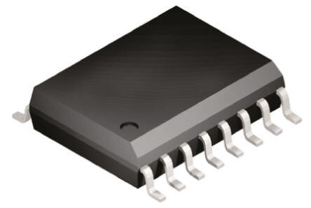
| 描述 | IC DGTL ISO 4CH LOGIC 16SOIC数字隔离器 5kV RMS Quad-CH Digital |
| 产品分类 | |
| IsolatedPower | 无 |
| 品牌 | Analog Devices |
| 产品手册 | |
| 产品图片 |
|
| rohs | 符合RoHS无铅 / 符合限制有害物质指令(RoHS)规范要求 |
| 产品系列 | 接口 IC,数字隔离器,Analog Devices ADUM4400CRWZiCoupler® |
| 数据手册 | |
| 产品型号 | ADUM4400CRWZ |
| PulseWidthDistortion(Max) | 2ns |
| 上升/下降时间(典型值) | 2.5ns, 2.5ns |
| 产品目录页面 | |
| 产品种类 | |
| 传播延迟tpLH/tpHL(最大值) | 32ns, 32ns |
| 传播延迟时间 | 32 ns |
| 供应商器件封装 | 16-SOIC W |
| 共模瞬态抗扰度(最小值) | 25kV/µs |
| 其它图纸 |
|
| 包装 | 管件 |
| 商标 | Analog Devices |
| 安装风格 | SMD/SMT |
| 封装 | Tube |
| 封装/外壳 | 16-SOIC(0.295",7.50mm 宽) |
| 封装/箱体 | SOIC-16 |
| 工作温度 | -40°C ~ 105°C |
| 工厂包装数量 | 47 |
| 技术 | 磁耦合 |
| 数据速率 | 90Mbps |
| 最大工作温度 | + 105 C |
| 最大数据速率 | 90 Mb/s |
| 最小工作温度 | - 40 C |
| 标准包装 | 47 |
| 电压-电源 | 2.7 V ~ 5.5 V |
| 电压-隔离 | 5000Vrms |
| 电源电压-最大 | 5.5 V |
| 电源电压-最小 | 2.7 V |
| 电源电流 | 0.83 mA |
| 类型 | General Purpose |
| 系列 | ADUM4400 |
| 绝缘电压 | 5 kVrms |
| 脉宽失真(最大) | 2ns |
| 视频文件 | http://www.digikey.cn/classic/video.aspx?PlayerID=1364138032001&width=640&height=505&videoID=2219593469001http://www.digikey.cn/classic/video.aspx?PlayerID=1364138032001&width=640&height=505&videoID=2219593470001http://www.digikey.cn/classic/video.aspx?PlayerID=1364138032001&width=640&height=505&videoID=2219614223001 |
| 输入-输入侧1/输入侧2 | 4/0 |
| 通道数 | 4 |
| 通道数量 | 4 Channel |
| 通道类型 | 单向 |
| 隔离式电源 | 无 |


- 商务部:美国ITC正式对集成电路等产品启动337调查
- 曝三星4nm工艺存在良率问题 高通将骁龙8 Gen1或转产台积电
- 太阳诱电将投资9.5亿元在常州建新厂生产MLCC 预计2023年完工
- 英特尔发布欧洲新工厂建设计划 深化IDM 2.0 战略
- 台积电先进制程称霸业界 有大客户加持明年业绩稳了
- 达到5530亿美元!SIA预计今年全球半导体销售额将创下新高
- 英特尔拟将自动驾驶子公司Mobileye上市 估值或超500亿美元
- 三星加码芯片和SET,合并消费电子和移动部门,撤换高东真等 CEO
- 三星电子宣布重大人事变动 还合并消费电子和移动部门
- 海关总署:前11个月进口集成电路产品价值2.52万亿元 增长14.8%


PDF Datasheet 数据手册内容提取
5 kV RMS Quad-Channel Digital Isolators Data Sheet ADuM4400/ADuM4401/ADuM4402 FEATURES GENERAL DESCRIPTION Enhanced system-level ESD performance per IEC 61000-4-x The ADuM440x1 are 4-channel digital isolators based on the Safety and regulatory approvals (RI-16 package) Analog Devices, Inc., iCoupler® technology. Combining high UL recognition: 5000 V rms for 1 minute per UL 1577 speed CMOS and monolithic air core transformer technology, CSA Component Acceptance Notice #5A these isolation components provide outstanding performance IEC 60601-1: 250 V rms (reinforced) characteristics that are superior to the alternatives, such as IEC 60950-1: 400 V rms (reinforced) optocoupler devices and other integrated couplers. VDE Certificate of Conformity The ADuM440x isolators provide four independent isolation DIN V VDE V 0884-10 (VDE V 0884-10):2006-12 channels in a variety of channel configurations and data rates V = 846 V peak IORM (see the Ordering Guide). All models operate with the supply Low power operation voltage on either side ranging from 3.0 V to 5.5 V, providing 5 V operation compatibility with lower voltage systems as well as enabling a 1.4 mA per channel maximum @ 0 Mbps to 2 Mbps voltage translation functionality across the isolation barrier. 4.3 mA per channel maximum @ 10 Mbps The ADuM440x isolators have a patented refresh feature that 34 mA per channel maximum @ 90 Mbps ensures dc correctness in the absence of input logic transitions 3.3 V operation and during power-up/power-down conditions. 0.9 mA per channel maximum @ 0 Mbps to 2 Mbps 2.4 mA per channel maximum @ 10 Mbps This family of isolators, like many Analog Devices isolators, 20 mA per channel maximum @ 90 Mbps offers very low power consumption, consuming one-tenth to Bidirectional communication one-sixth the power of comparable isolators at comparable data 3.3 V/5 V level translation rates up to 10 Mbps. All models of the ADuM440x provide low High temperature operation: 105°C pulse width distortion (<2 ns for C grade). In addition, every High data rate: dc to 90 Mbps (NRZ) model has an input glitch filter to protect against extraneous Precise timing characteristics noise disturbances. 2 ns maximum pulse width distortion The ADuM440x contain circuit and layout enhancements to help 2 ns maximum channel-to-channel matching achieve system-level IEC 61000-4-x compliance (ESD/burst/surge). High common-mode transient immunity: >25 kV/µs The precise capability in these tests for the ADuM440x are strongly Output enable function determined by the design and layout of the user’s board or module. 16-lead SOIC wide body package version (RW-16) For more information, see the AN-793 Application Note, 16-lead SOIC wide body enhanced creepage version (RI-16) ESD/Latch-Up Considerations with iCoupler Isolation Products. APPLICATIONS 1 Protected by U.S. Patents 5,952,849; 6,873,065; and 7,075,329. General-purpose, high voltage, multichannel isolation Medical equipment Motor drives Power supplies FUNCTIONAL BLOCK DIAGRAMS VDD1 1 ADuM4400 16VDD2 VDD1 1 ADuM4401 16VDD2 VDD1 1 ADuM4402 16VDD2 GND1 2 15GND2 GND1 2 15GND2 GND1 2 15GND2 VIA 3 ENCODE DECODE 14VOA VIA 3 ENCODE DECODE 14VOA VIA 3 ENCODE DECODE 14VOA VIB 4 ENCODE DECODE 13VOB VIB 4 ENCODE DECODE 13VOB VIB 4 ENCODE DECODE 13VOB VIC 5 ENCODE DECODE 12VOC VIC 5 ENCODE DECODE 12VOC VOC 5 DECODE ENCODE 12VIC VID 6 ENCODE DECODE 11VOD VOD 6 DECODE ENCODE 11VID VOD 6 DECODE ENCODE 11VID GNNDC1 87 190VGEN2D2 08157-001 GNVDE11 87 190VGEN2D2 08157-002 GNVDE11 87 190VGEN2D2 08157-003 Figure 1. ADuM4400 Figure 2. ADuM4401 Figure 3. ADuM4402 Rev. F Document Feedback Information furnished by Analog Devices is believed to be accurate and reliable. However, no responsibility is assumed by Analog Devices for its use, nor for any infringements of patents or other One Technology Way, P.O. Box 9106, Norwood, MA 02062-9106, U.S.A. rights of third parties that may result from its use. Specifications subject to change without notice. No license is granted by implication or otherwise under any patent or patent rights of Analog Devices. Tel: 781.329.4700 ©2009–2017 Analog Devices, Inc. All rights reserved. Trademarks and registered trademarks are the property of their respective owners. Technical Support www.analog.com
ADuM4400/ADuM4401/ADuM4402 Data Sheet TABLE OF CONTENTS Features .............................................................................................. 1 Recommended Operating Conditions .......................................9 Applications ....................................................................................... 1 Absolute Maximum Ratings ......................................................... 10 General Description ......................................................................... 1 ESD Caution................................................................................ 10 Functional Block Diagrams ............................................................. 1 Pin Configurations and Function Descriptions ......................... 11 Revision History ............................................................................... 2 Typical Performance Characteristics ........................................... 14 Specifications ..................................................................................... 3 Applications Information .............................................................. 16 Electrical Characteristics—5 V Operation................................ 3 PC Board Layout ........................................................................ 16 Electrical Characteristics—3.3 V Operation ............................ 4 System-Level ESD Considerations and Enhancements ........ 16 Electrical Characteristics—Mixed 5 V/3.3 V Operation ........ 5 Propagation Delay-Related Parameters ................................... 16 Electrical Characteristics—Mixed 3.3 V/5 V Operation ........ 6 DC Correctness and Magnetic Field Immunity ..................... 16 Package Characteristics ............................................................... 7 Power Consumption .................................................................. 17 Regulatory Information ............................................................... 7 Insulation Lifetime ..................................................................... 18 Insulation and Safety-Related Specifications ............................ 8 Outline Dimensions ....................................................................... 19 DIN V VDE V 0884-10 (VDE V 0884-10) Insulation Ordering Guide .......................................................................... 20 Characteristics .............................................................................. 9 REVISION HISTORY 7/2017—Rev. E to Rev. F 10/2011—Rev. A to Rev. B Change to Logic High Output Voltage Parameter and Logic low Added Logic Low Output Voltage, Table 3 .................................... 3 Output Voltage Parameter; Table 3 ................................................ 3 Added Logic Low Output Voltage, Table 6 .................................... 4 Change to Logic High Output Voltage Parameter and Logic low Added Logic Low Output Voltage, Table 9 .................................... 5 Output Voltage Parameter; Table 6 ................................................ 4 Added Logic Low Output Voltage, Table 12 .................................. 6 Change to Logic High Output Voltage Parameter and Logic low Output Voltage Parameter; Table 9 ................................................ 5 8/2011—Rev. 0 to Rev. A Change to Logic High Output Voltage Parameter and Logic low Added 16-Lead SOIC_IC Package ................................... Universal Output Voltage Parameter; Table 12 .............................................. 6 Changes to Features Section ............................................................ 1 Changes to Pulse Width Parameter, C Grade, Table 1 ................. 3 5/2017—Rev. D to Rev. E Changes to Pulse Width Parameter, C Grade, Table 4 ................. 4 Changes to Table 14 .......................................................................... 7 Changes to Pulse Width Parameter, C Grade, Table 7 ................. 5 Changes to Pulse Width Parameter, C Grade, Table 10 ............... 6 9/2016—Rev. C to Rev. D Changes to Table 14 and Table 15 ................................................... 7 Changed 3.0 V to 3.3 V and 2.7 V to 3.0 V ................ Throughout Deleted (Pending) Throughout ....................................................... 8 Changes to Figure 8 to Figure 13 .................................................. 13 Changes to Endnote 1, Table 17 ...................................................... 8 Changes to Figure 14 to Figure 16 ................................................ 14 Updated Outline Dimensions ....................................................... 18 Updated Outline Dimensions ....................................................... 18 Changes to Ordering Guide .......................................................... 19 Changes to Ordering Guide .......................................................... 19 4/2009—Revision 0: Initial Version 2/2012—Rev. B to Rev. C Created Hyperlink for Safety and Regulatory Approvals Entry in Features Section ................................................................. 1 Change to PC Board Layout Section ............................................ 15 Rev. F | Page 2 of 21
Data Sheet ADuM4400/ADuM4401/ADuM4402 SPECIFICATIONS ELECTRICAL CHARACTERISTICS—5 V OPERATION All typical specifications are at T = 25°C, V = V = 5 V. Minimum/maximum specifications apply over the entire recommended A DD1 DD2 operation range of 4.5 V ≤ V ≤ 5.5 V, 4.5 V ≤ V ≤ 5.5 V, and −40°C ≤ T ≤ 105°C, unless otherwise noted. Switching specifications DD1 DD2 A are tested with C = 15 pF and CMOS signal levels, unless otherwise noted. L Table 1. A Grade B Grade C Grade Parameter Symbol Min Typ Max Min Typ Max Min Typ Max Unit Test Conditions SWITCHING SPECIFICATIONS Data Rate 1 10 90 Mbps Within PWD limit Propagation Delay t t 50 65 100 20 32 50 18 27 32 ns 50% input to 50% output PHL, PLH Pulse Width Distortion PWD 40 3 0.5 2 ns |t − t | PLH PHL Change vs. Temperature 11 5 3 ps/°C Pulse Width PW 1000 100 11.1 ns Within PWD limit Propagation Delay Skew t 50 15 10 ns Between any two units PSK Channel Matching Codirectional t 50 3 2 ns PSKCD Opposing-Direction t 50 6 5 ns PSKOD Table 2. 1 Mbps—A, B, C Grades 10 Mbps—B, C Grades 90 Mbps—C Grade Parameter Symbol Min Typ Max Min Typ Max Min Typ Max Unit Test Conditions SUPPLY CURRENT ADuM4400 I 2.9 3.5 9.0 11.6 72 100 mA DD1 I 1.2 1.9 3.0 5.5 19 36 mA DD2 ADuM4401 I 2.5 3.2 7.4 10.6 59 82 mA DD1 I 1.6 2.4 4.4 6.5 32 46 mA DD2 ADuM4402 I 2.0 2.8 6.0 7.5 51 62 mA DD1 I 2.0 2.8 6.0 7.5 51 62 mA DD2 Table 3. For All Models Parameter Symbol Min Typ Max Unit Test Conditions DC SPECIFICATIONS Logic High Input Threshold VIH 2.0 V Logic Low Input Threshold VIL 0.8 V Logic High Output Voltage V V − 0.1 5.0 V I = −20 µA, V = V OH DDx Ox Ix IxH V − 0.4 4.8 V I = −3.2 mA, V = V DDx Ox Ix IxH Logic Low Output Voltage V 0.0 0.1 V I = 20 µA, V = V OL Ox Ix IxL 0.04 0.1 V I = 400 µA, V = V Ox Ix IxL 0.2 0.4 V I = 3.2 mA, V = V Ox Ix IxL Input Current per Channel I −10 +0.01 +10 µA 0 V ≤ V ≤ V I Ix DDx Supply Current per Channel Quiescent Input Supply Current I 0.57 0.83 mA DDI(Q) Quiescent Output Supply Current I 0.23 0.35 mA DDO(Q) Dynamic Input Supply Current I 0.20 mA/Mbps DDI(D) Dynamic Output Supply Current I 0.05 mA/Mbps DDO(D) AC SPECIFICATIONS Output Rise/Fall Time t/t 2.5 ns 10% to 90% R F Common-Mode Transient Immunity1 |CM| 25 35 kV/µs V = V , V = 1000 V, Ix DDx CM transient magnitude = 800 V Output Disable Propagation Delay t , t 6 8 ns High/low-to-high impedance PHZ PLH Output Enable Propagation Delay t , t 6 8 ns High impedance-to-high/low PZH PZL Refresh Rate f 1.2 Mbps r 1 |CM| is the maximum common-mode voltage slew rate that can be sustained while maintaining VO > 0.8 VDD. The common-mode voltage slew rates apply to both rising and falling common-mode voltage edges. Rev. F | Page 3 of 21
ADuM4400/ADuM4401/ADuM4402 Data Sheet ELECTRICAL CHARACTERISTICS—3.3 V OPERATION All typical specifications are at T = 25°C, V = V = 3.3 V. Minimum/maximum specifications apply over the entire recommended A DD1 DD2 operation range: 3.0 V ≤ V ≤ 3.6 V, 3.0 V ≤ V ≤ 3.6 V, and −40°C ≤ T ≤ 105°C, unless otherwise noted. Switching specifications are DD1 DD2 A tested with C = 15 pF and CMOS signal levels, unless otherwise noted. L Table 4. A Grade B Grade C Grade Parameter Symbol Min Typ Max Min Typ Max Min Typ Max Unit Test Conditions SWITCHING SPECIFICATIONS Data Rate 1 10 90 Mbps Within PWD limit Propagation Delay t , t 50 75 100 20 38 50 20 34 45 ns 50% input to 50% output PHL PLH Pulse Width Distortion PWD 40 3 0.5 2 ns |t − t | PLH PHL Change vs. Temperature 11 5 3 ps/°C Pulse Width PW 1000 100 11.1 ns Within PWD limit Propagation Delay Skew t 50 22 16 ns Between any two units PSK Channel Matching Codirectional t 50 3 2 ns PSKCD Opposing-Direction t 50 6 5 ns PSKOD Table 5. 1 Mbps—A, B, C Grades 10 Mbps—B, C Grades 90 Mbps—C Grade Parameter Symbol Min Typ Max Min Typ Max Min Typ Max Unit Test Conditions SUPPLY CURRENT ADuM4400 I 1.6 2.1 4.8 7.1 37 54 mA DD1 I 0.7 1.2 1.8 2.3 11 15 mA DD2 ADuM4401 I 1.4 1.9 0.1 5.6 31 44 mA DD1 I 0.9 1.5 2.5 3.3 17 24 mA DD2 ADuM4402 I 1.2 1.7 3.3 4.4 24 39 mA DD1 I 1.2 1.7 3.3 4.4 24 39 mA DD2 Table 6. For All Models Parameter Symbol Min Typ Max Unit Test Conditions DC SPECIFICATIONS Logic High Input Threshold VIH 1.6 V Logic Low Input Threshold VIL 0.4 V Logic High Output Voltage V V − 0.1 3.0 V I = −20 µA, V = V OH DDx Ox Ix IxH VDDx − 0.4 2.8 V IOx = −3.2 mA, VIx = VIxH Logic Low Output Voltage V 0.0 0.1 V I = 20 µA, V = V OL Ox Ix IxL 0.04 0.1 V I = 400 µA, V = V Ox Ix IxL 0.2 0.4 V I = 3.2 mA, V = V Ox Ix IxL Input Current per Channel II −10 +0.01 +10 µA 0 V ≤ VIx ≤ VDDx Supply Current per Channel Quiescent Input Supply Current I 0.31 0.49 mA DDI(Q) Quiescent Output Supply Current I 0.19 0.27 mA DDO(Q) Dynamic Input Supply Current I 0.10 mA/Mbps DDI(D) Dynamic Output Supply Current I 0.03 mA/Mbps DDO(D) AC SPECIFICATIONS Output Rise/Fall Time t/t 3 ns 10% to 90% R F Common-Mode Transient Immunity1 |CM| 25 35 kV/µs V = V , V = 1000 V, Ix DDx CM transient magnitude = 800 V Output Disable Propagation Delay t , t 6 8 ns High/low-to-high impedance PHZ PLH Output Enable Propagation Delay t , t 6 8 ns High impedance-to-high/low PZH PZL Refresh Rate f 1.2 Mbps r 1 |CM| is the maximum common-mode voltage slew rate that can be sustained while maintaining VO > 0.8 VDD. The common-mode voltage slew rates apply to both rising and falling common-mode voltage edges. Rev. F | Page 4 of 21
Data Sheet ADuM4400/ADuM4401/ADuM4402 ELECTRICAL CHARACTERISTICS—MIXED 5 V/3.3 V OPERATION All typical specifications are at T = 25°C, V = 5 V, V = 3.3 V. Minimum/maximum specifications apply over the entire recommended A DD1 DD2 operation range: 4.5 V ≤ V ≤ 5.5 V, 3.0 V ≤ V ≤ 3.6 V, and −40°C ≤ T ≤ 105°C, unless otherwise noted. Switching specifications are DD1 DD2 A tested with C = 15 pF and CMOS signal levels, unless otherwise noted. L Table 7. A Grade B Grade C Grade Parameter Symbol Min Typ Max Min Typ Max Min Typ Max Unit Test Conditions SWITCHING SPECIFICATIONS Data Rate 1 10 90 Mbps Within PWD limit Propagation Delay t , t 50 70 50 15 35 50 20 30 40 ns 50% input to 50% output PHL PLH Pulse Width Distortion PWD 40 3 0.5 2 ns |t − t | PLH PHL Change vs. Temperature 11 5 3 ps/°C Pulse Width PW 1000 100 11.1 ns Within PWD limit Propagation Delay Skew t 50 22 14 ns Between any two units PSK Channel Matching Codirectional t 50 3 2 ns PSKCD Opposing-Direction t 50 6 5 ns PSKOD Table 8. 1 Mbps—A, B, C Grades 10 Mbps—B, C Grades 90 Mbps—C Grade Parameter Symbol Min Typ Max Min Typ Max Min Typ Max Unit Test Conditions SUPPLY CURRENT ADuM4400 I 2.9 3.5 9.0 11.6 72 100 mA DD1 I 0.7 1.2 1.8 2.3 11 15 mA DD2 ADuM4401 I 2.5 3.2 7.4 10.6 59 82 mA DD1 I 0.9 1.5 2.5 3.3 17 24 mA DD2 ADuM4402 I 2.0 2.8 6.0 7.5 46 62 mA DD1 I 1.2 1.7 3.3 4.4 24 39 mA DD2 Table 9. For All Models Parameter Symbol Min Typ Max Unit Test Conditions DC SPECIFICATIONS Logic High Input Threshold VIH 2.0 V Logic Low Input Threshold VIL 0.8 V Logic High Output Voltage V V − 0.1 3.0 V I = −20 µA, V = V OH DDx Ox Ix IxH V − 0.4 2.8 V I = −3.2 mA, V = V DDx Ox Ix IxH Logic Low Output Voltage V 0.0 0.1 V I = 20 µA, V = V OL Ox Ix IxL 0.04 0.1 V I = 400 µA, V = V Ox Ix IxL 0.2 0.4 V I = 3.2 mA, V = V Ox Ix IxL Input Current per Channel I −10 +0.01 +10 µA 0 V ≤ V ≤ V I Ix DDx Supply Current per Channel Quiescent Input Supply Current I 0.57 0.83 mA DDI(Q) Quiescent Output Supply Current I 0.29 0.27 mA DDO(Q) Dynamic Input Supply Current I 0.20 mA/Mbps DDI(D) Dynamic Output Supply Current I 0.03 mA/Mbps DDO(D) AC SPECIFICATIONS Output Rise/Fall Time t/t 3 ns 10% to 90% R F Common-Mode Transient Immunity1 |CM| 25 35 kV/µs V = V , V = 1000 V, Ix DDx CM transient magnitude = 800 V Output Disable Propagation Delay t , t 6 8 ns High/low-to-high impedance PHZ PLH Output Enable Propagation Delay t , t 6 8 ns High impedance-to-high/low PZH PZL Refresh Rate f 1.2 Mbps r 1 |CM| is the maximum common-mode voltage slew rate that can be sustained while maintaining VO > 0.8 VDD. The common-mode voltage slew rates apply to both rising and falling common-mode voltage edges. Rev. F | Page 5 of 21
ADuM4400/ADuM4401/ADuM4402 Data Sheet ELECTRICAL CHARACTERISTICS—MIXED 3.3 V/5 V OPERATION All typical specifications are at T = 25°C, V = 3.3 V, V = 5 V. Minimum/maximum specifications apply over the entire recommended A DD1 DD2 operation range: 3.0 V ≤ V ≤ 3.6 V, 4.5 V ≤ V ≤ 5.5 V, and −40°C ≤ T ≤ +105°C, unless otherwise noted. Switching specifications DD1 DD2 A are tested with C = 15 pF and CMOS signal levels, unless otherwise noted. L Table 10. A Grade B Grade C Grade Parameter Symbol Min Typ Max Min Typ Max Min Typ Max Unit Test Conditions SWITCHING SPECIFICATIONS Data Rate 1 10 90 Mbps Within PWD limit Propagation Delay t , t 50 70 100 15 35 50 20 30 40 ns 50% input to 50% output PHL PLH Pulse Width Distortion PWD 40 3 0.5 2 ns |t − t | PLH PHL Change vs. Temperature 11 5 3 ps/°C Pulse Width PW 1000 100 11.1 ns Within PWD limit Propagation Delay Skew t 50 22 14 ns Between any two units PSK Channel Matching Codirectional t 50 3 2 ns PSKCD Opposing-Direction t 50 6 5 ns PSKOD Table 11. 1 MBps—A, B, C Grades 10 MBps—B, C Grades 90 MBps—C Grade Parameter Symbol Min Typ Max Min Typ Max Min Typ Max Unit Test Conditions SUPPLY CURRENT ADuM4400 IDD1 1.6 2.1 4.8 7.1 37 54 mA IDD2 1.2 1.9 3.0 5.5 19 36 mA ADuM4401 IDD1 1.4 1.9 4.1 5.6 31 44 mA IDD2 1.6 2.4 4.4 6.5 32 46 mA ADuM4402 IDD1 1.2 1.7 3.3 4.4 24 39 mA IDD2 2.0 2.8 6.0 7.5 46 62 mA Table 12. For All Models Parameter Symbol Min Typ Max Unit Test Conditions DC SPECIFICATIONS Logic High Input Threshold VIH 1.6 V Logic Low Input Threshold VIL 0.4 V Logic High Output Voltage V V − 0.1 5.0 V I = −20 µA, V = V OH DDx Ox Ix IxH V − 0.4 4.8 V I = −3.2 mA, V = V DDx Ox Ix IxH Logic Low Output Voltage V 0.0 0.1 V I = 20 µA, V = V OL Ox Ix IxL 0.04 0.1 V I = 400 µA, V = V Ox Ix IxL 0.2 0.4 V I = 3.2 mA, V = V Ox Ix IxL Input Current per Channel I −10 +0.01 +10 µA 0 V ≤ V ≤ V I Ix DDx Supply Current per Channel Quiescent Input Supply Current I 0.31 0.49 mA DDI(Q) Quiescent Output Supply Current I 0.19 0.35 mA DDO(Q) Dynamic Input Supply Current I 0.10 mA/Mbps DDI(D) Dynamic Output Supply Current I 0.05 mA/Mbps DDO(D) AC SPECIFICATIONS Output Rise/Fall Time t/t 2.5 ns 10% to 90% R F Common-Mode Transient Immunity1 |CM| 25 35 kV/µs V = V , V = 1000 V, Ix DDx CM transient magnitude = 800 V Output Disable Propagation Delay t , t 6 8 ns High/low-to-high impedance PHZ PLH Output Enable Propagation Delay t , t 6 8 ns High impedance-to-high/low PZH PZL Refresh Rate f 1.1 Mbps r 1 |CM| is the maximum common-mode voltage slew rate that can be sustained while maintaining VO > 0.8 VDD. The common-mode voltage slew rates apply to both rising and falling common-mode voltage edges. Rev. F | Page 6 of 21
Data Sheet ADuM4400/ADuM4401/ADuM4402 PACKAGE CHARACTERISTICS Table 13. Parameter Symbol Min Typ Max Unit Test Conditions Resistance (Input to Output)1 R 1012 Ω I-O Capacitance (Input to Output)1 C 2.2 pF f = 1 MHz I-O Input Capacitance2 C 4.0 pF I IC Junction-to-Case Thermal Resistance, Side 1 θ 33 °C/W Thermocouple located at JCI IC Junction-to-Case Thermal Resistance, Side 2 θ 28 °C/W center of package underside JCO 1 Device considered a 2-terminal device: Pin 1, Pin 2, Pin 3, Pin 4, Pin 5, Pin 6, Pin 7, and Pin 8 shorted together and Pin 9, Pin 10, Pin 11, Pin 12, Pin 13, Pin 14, Pin 15, and Pin 16 shorted together. 2 Input capacitance is from any input data pin to ground. REGULATORY INFORMATION The ADuM440x are approved by the organizations listed in Table 14. Refer to Table 19 and the Insulation Lifetime section for details regarding recommended maximum working voltages for specific cross-isolation waveforms and insulation levels. Table 14. UL CSA VDE CQC Recognized under Approved under CSA Component Certified according to Approved under CQC11-471543-2015 1577 Component Acceptance Notice #5A DIN V VDE V 0884-10 Recognition (VDE V 0884-10): 2006- Program1 122 Single Protection Basic insulation per CSA 60950-1-07 and IEC Reinforced insulation, 5000 V rms 60950-1, 600 V rms (848 V peak) maximum 846 V peak Isolation Voltage working voltage RW-16 package RW-16 package Reinforced insulation per CSA 60950-1-07 Basic insulation per GB4943.1-2011, and IEC 60950-1, 380 V rms (537 V peak) 760 V rms (1075 V peak) maximum maximum working voltage; reinforced working voltage, tropical climate, insulation per IEC 60601-1 125 V rms altitude ≤ 5000 m (176 V peak) maximum working voltage Reinforced insulation per GB4943.1-2011, 380 V rms (537 V peak) maximum working voltage, tropical climate, altitude ≤ 5000 m RI-16 package RI-16 Package Reinforced insulation per CSA 60950-1-07 Basic insulation per GB4943.1-2011, and IEC 60950-1, 400 V rms (565 V peak) 820 V rms (1159 V peak) maximum maximum working voltage; reinforced working voltage, tropical climate, insulation per IEC 60601-1 250 V rms altitude ≤ 5000 m (353 V peak) maximum working voltage Reinforced insulation per GB4943.1-2011, 401 V rms (578 V peak) maximum working voltage, tropical climate, altitude ≤ 5000 m File E214100 File 205078 File 2471900-4880-0001 File CQC16001150402 1 In accordance with UL1577, each ADuM440x is proof tested by applying an insulation test voltage ≥ 6000 V rms for 1 second (current leakage detection limit = 10 µA). 2 In accordance with DIN V VDE V 0884-10, each ADuM440x is proof tested by applying an insulation test voltage ≥1590 V peak for 1 sec (partial discharge detection limit = 5 pC). The * marking branded on the component designates DIN V VDE V 0884-10 approval. Rev. F | Page 7 of 21
ADuM4400/ADuM4401/ADuM4402 Data Sheet INSULATION AND SAFETY-RELATED SPECIFICATIONS Table 15. Parameter Symbol Value Unit Conditions Rated Dielectric Insulation Voltage 5000 V rms 1-minute duration Minimum External Air Gap L(I01) 8.0 min mm Distance measured from input terminals to output terminals, shortest distance through air along the PCB mounting plane, as an aid to PC board layout Minimum External Tracking (Creepage) RW-16 Package L(I02) 7.7 min mm Measured from input terminals to output terminals, shortest distance path along body Minimum External Tracking (Creepage) RI-16 Package L(I02) 8.3 min mm Measured from input terminals to output terminals, shortest distance path along body Minimum Internal Gap (Internal Clearance) 0.017 min mm Insulation distance through insulation Tracking Resistance (Comparative Tracking Index) CTI >175 V DIN IEC 112/VDE 0303 Part 1 Rev. F | Page 8 of 21
Data Sheet ADuM4400/ADuM4401/ADuM4402 DIN V VDE V 0884-10 (VDE V 0884-10) INSULATION CHARACTERISTICS These isolators are suitable for reinforced electrical isolation only within the safety limit data. Maintenance of the safety data is ensured by means of protective circuits. Note that the * marking on packages denotes DIN V VDE V 0884-10 approval for 846 V peak working voltage. Table 16. Description Conditions Symbol Characteristic Unit Installation Classification per DIN VDE 0110 For Rated Mains Voltage ≤ 300 V rms I to IV For Rated Mains Voltage ≤ 450 V rms I to II For Rated Mains Voltage ≤ 600 V rms I to II Climatic Classification 40/105/21 Pollution Degree (DIN VDE 0110, Table 1) 2 Maximum Working Insulation Voltage V 846 V peak IORM Input-to-Output Test Voltage, Method b1 V × 1.875 = V , 100% production test, t = 1 sec, V 1590 V peak IORM PR m PR partial discharge < 5 pC Input-to-Output Test Voltage, Method a V PR After Environmental Tests Subgroup 1 V × 1.6 = V , t = 60 sec, partial discharge < 5 pC 1375 V peak IORM PR m After Input and/or Safety Test Subgroup 2 V × 1.2 = V , t = 60 sec, partial discharge < 5 pC 1018 V peak IORM PR m and Subgroup 3 Highest Allowable Overvoltage Transient overvoltage, t = 10 seconds V 6000 V peak TR TR Safety-Limiting Values Maximum value allowed in the event of a failure; see Figure 4 Case Temperature T 150 °C S Side 1 Current I 265 mA S1 Side 2 Current I 335 mA S2 Insulation Resistance at T V = 500 V R >109 Ω S IO S 350 RECOMMENDED OPERATING CONDITIONS 300 Table 17. A) m Parameter Symbol Min Max Unit T ( 250 N Operating Temperature T −40 +105 °C E SIDE #2 A R UR 200 Supply Voltages1 VDD1, VDD2 3.0 5.5 V C G Input Signal Rise and Fall Times 1.0 ms N TI 150 MI SIDE #1 1 All voltages are relative to their respective ground. LI Y- 100 T E F A S 50 00 50CASE TEMP1E0R0ATURE (°C)150 200 08157-004 Figure 4. Thermal Derating Curve, Dependence of Safety Limiting Values with Case Temperature per DIN V VDE V 0884-10 Rev. F | Page 9 of 21
ADuM4400/ADuM4401/ADuM4402 Data Sheet ABSOLUTE MAXIMUM RATINGS Table 18. Stresses at or above those listed under Absolute Maximum Parameter Rating Ratings may cause permanent damage to the product. This is a Storage Temperature (T ) −65°C to +150°C stress rating only; functional operation of the product at these ST Ambient Operating Temperature (T ) −40°C to +105°C or any other conditions above those indicated in the operational A Supply Voltages (V , V )1 −0.5 V to +7.0 V section of this specification is not implied. Operation beyond DD1 DD2 Input Voltage (V , V , V , V , V , V )1, 2 −0.5 V to V + 0.5 V the maximum operating conditions for extended periods may IA IB IC ID E1 E2 DDI Output Voltage (V , V , V , V )1, 2 −0.5 V to V + 0.5 V affect product reliability. OA OB OC OD DDO Average Output Current Per Pin3 Side 1 (I ) −18 mA to +18 mA O1 ESD CAUTION Side 2 (I ) −22 mA to +22 mA O2 Common-Mode Transients4 −100 kV/µs to +100 kV/µs 1 All voltages are relative to their respective ground. 2 VDDI and VDDO refer to the supply voltages on the input and output sides of a given channel, respectively. See the PC Board Layout section. 3 See Figure 4 for maximum rated current values for various temperatures. 4 Refers to common-mode transients across the insulation barrier. Common- mode transients exceeding the Absolute Maximum Rating can cause latch- up or permanent damage. Table 19. Maximum Continuous Working Voltage1 Parameter Max Unit Constraint AC Voltage, Bipolar Waveform 565 V peak 50 year minimum lifetime AC Voltage, Unipolar Waveform Reinforced Insulation 846 V peak Maximum approved working voltage per IEC 60950-1 and VDE V 0884-10 DC Voltage Reinforced Insulation 846 V peak Maximum approved working voltage per IEC 60950-1 and VDE V 0884-10 1 Refers to continuous voltage magnitude imposed across the isolation barrier. See the Insulation Lifetime section for more details. Table 20. Truth Table (Positive Logic) V Input1 V Input V State1 V State1 V Output1 Notes Ix Ex DDI DDO Ox H H or NC Powered Powered H L H or NC Powered Powered L X L Powered Powered Z X H or NC Unpowered Powered H Outputs return to input state within 1 µs of V power restoration. DDI X L Unpowered Powered Z X X Powered Unpowered Indeterminate Outputs return to input state within 1 µs of V power restoration if DDO V state is H or NC. Outputs return to high impedance state within Ex 8 ns of V power restoration if V state is L. DDO Ex 1 VIx and VOx refer to the input and output signals of a given channel (A, B, C, or D). VEx refers to the output enable signal on the same side as the VOx outputs. VDDI and VDDO refer to the supply voltages on the input and output sides of the given channel, respectively. Rev. F | Page 10 of 21
Data Sheet ADuM4400/ADuM4401/ADuM4402 PIN CONFIGURATIONS AND FUNCTION DESCRIPTIONS VDD1 1 16 VDD2 GND1 2 15 GND2 VIA 3 ADuM4400 14 VOA VIB 4 TOP VIEW 13 VOB VIC 5 (Not to Scale) 12 VOC VID 6 11 VOD NC 7 10 VE2 GND1 8 9 GND2 NOTES 1. NC = NO CONNECT 2. PIN 2AND PIN 8ARE INTERNALLY CONNECTED, 3. AAPNNINDD 9 CCAOONNNDNN PEEICCNTT 1IINN5GGA RBBEOO ITTNHHTETTOORN GGANNLDDL12Y IICSSO RRNEENCCEOOCMMTMMEEEDNN,DDEEDD.. 08157-005 Figure 5. ADuM4400 Pin Configuration Table 21. ADuM4400 Pin Function Descriptions Pin No. Mnemonic Description 1 V Supply Voltage for Isolator Side 1, 3.0 V to 5.5 V. DD1 2 GND Ground 1. Ground reference for isolator Side 1. 1 3 V Logic Input A. IA 4 V Logic Input B. IB 5 V Logic Input C. IC 6 V Logic Input D. ID 7 NC No Connect. 8 GND Ground 1. Ground reference for isolator Side 1. 1 9 GND Ground 2. Ground reference for isolator Side 2. 2 10 V Output Enable 2. Active high logic input. V outputs on Side 2 are enabled when V is high or disconnected. E2 Ox E2 V Side 2 outputs are disabled when V is low. In noisy environments, connecting V to an external logic high or low Ox E2 E2 is recommended. 11 V Logic Output D. OD 12 V Logic Output C. OC 13 V Logic Output B. OB 14 V Logic Output A. OA 15 GND Ground 2. Ground reference for isolator Side 2. 2 16 V Supply Voltage for Isolator Side 2, 3.0 V to 5.5 V. DD2 Rev. F | Page 11 of 21
ADuM4400/ADuM4401/ADuM4402 Data Sheet VDD1 1 16 VDD2 GND1 2 15 GND2 VIA 3 ADuM4401 14 VOA VIB 4 TOP VIEW 13 VOB VIC 5 (Not to Scale) 12 VOC VOD 6 11 VID VE1 7 10 VE2 GND1 8 9 GND2 NOTES 1. PIN 2AND PIN 8ARE INTERNALLY CONNECTED, 2. AAPNNINDD 9 CCAOONNNDNN PEEICCNTT 1IINN5GGA RBBEOO ITTNHHTETTOORN GGANNLDDL12Y IICSSO RRNEENCCEOOCMMTMMEEEDNN,DDEEDD.. 08157-006 Figure 6. ADuM4401 Pin Configuration Table 22. ADuM4401 Pin Function Descriptions Pin No. Mnemonic Description 1 V Supply Voltage for Isolator Side 1, 3.0 V to 5.5 V. DD1 2 GND Ground 1. Ground reference for isolator Side 1. 1 3 V Logic Input A. IA 4 V Logic Input B. IB 5 V Logic Input C. IC 6 V Logic Output D. OD 7 V Output Enable. Active high logic input. V Side 1 outputs are enabled when V is high or disconnected. V Side 1 E1 Ox E1 OX outputs are disabled when V is low. In noisy environments, connecting V to an external logic high or low is E1 E1 recommended. 8 GND Ground 1. Ground reference for isolator Side 1. 1 9 GND Ground 2. Ground reference for isolator Side 2. 2 10 V Output Enable 2. Active high logic input. V outputs on Side 2 are enabled when V is high or disconnected. E2 Ox E2 V Side 2 outputs are disabled when V is low. In noisy environments, connecting V to an external logic high or low Ox E2 E2 is recommended. 11 V Logic Input D. ID 12 V Logic Output C. OC 13 V Logic Output B. OB 14 V Logic Output A. OA 15 GND Ground 2. Ground reference for isolator Side 2. 2 16 V Supply Voltage for Isolator Side 2, 3.0 V to 5.5 V. DD2 Rev. F | Page 12 of 21
Data Sheet ADuM4400/ADuM4401/ADuM4402 VDD1 1 16 VDD2 GND1 2 15 GND2 VIA 3 ADuM4402 14 VOA VIB 4 TOP VIEW 13 VOB VOC 5 (Not to Scale) 12 VIC VOD 6 11 VID VE1 7 10 VE2 GND1 8 9 GND2 NOTES 1. PIN 2AND PIN 8ARE INTERNALLY CONNECTED, 2. AAPNNINDD 9 CCAOONNNDNN PEEICCNTT 1IINN5GGA RBBEOO ITTNHHTETTOORN GGANNLDDL12Y IICSSO RRNEENCCEOOCMMTMMEEEDNN,DDEEDD.. 08157-007 Figure 7. ADuM4402 Pin Configuration Table 23. ADuM4402 Pin Function Descriptions Pin No. Mnemonic Description 1 V Supply Voltage for Isolator Side 1, 3.0 V to 5.5 V. DD1 2 GND Ground 1. Ground reference for isolator Side 1. 1 3 V Logic Input A. IA 4 V Logic Input B. IB 5 V Logic Output C. OC 6 V Logic Output D. OD 7 V Output Enable 1. Active high logic input. V Side 1 outputs are enabled when V is high or disconnected. V Side 1 E1 Ox E1 OX outputs are disabled when V is low. In noisy environments, connecting V to an external logic high or low is E1 E1 recommended. 8 GND Ground 1. Ground reference for isolator Side 1. 1 9 GND Ground 2. Ground reference for isolator Side 2. 2 10 V Output Enable 2. Active high logic input. V outputs on Side 2 are enabled when V is high or disconnected. E2 Ox E2 V Side 2 outputs are disabled when V is low. In noisy environments, connecting V to an external logic high or Ox E2 E2 low is recommended. 11 V Logic Input D. ID 12 V Logic Input C. IC 13 V Logic Output B. OB 14 V Logic Output A. OA 15 GND Ground 2. Ground reference for isolator Side 2. 2 16 V Supply Voltage for Isolator Side 2, 3.0 V to 5.5 V. DD2 Rev. F | Page 13 of 21
ADuM4400/ADuM4401/ADuM4402 Data Sheet TYPICAL PERFORMANCE CHARACTERISTICS 20 80 15 60 A) m NEL ( 5.0V mA) T/CHAN 10 RRENT ( 40 5.0V N U RE 3.3V C 3.3V R CU 5 20 00 20 DA4T0A RATE (Mb60ps) 80 100 08157-008 00 20 DA4T0A RATE (Mb60ps) 80 100 08157-011 Figure 8. Typical Input Supply Current per Channel vs. Data Rate (No Load) Figure 11. Typical ADuM4400 VDD1 Supply Current vs. Data Rate for 5 V and 3.3 V Operation 20 80 15 60 A) m NEL ( mA) T/CHAN 10 RRENT ( 40 N U RE C R CU 5 20 5.0V 5.0V 3.3V 3.3V 00 20 DA4T0A RATE (Mb60ps) 80 100 08157-009 00 20 DA4T0A RATE (Mb60ps) 80 100 08157-012 Figure 9. Typical Output Supply Current per Channel vs. Data Rate (No Load) Figure 12. Typical ADuM4400 VDD2 Supply Current vs. Data Rate for 5 V and 3 V Operation 20 80 15 60 A) m NEL ( mA) T/CHAN 10 RRENT ( 40 5.0V REN 5.0V CU R CU 5 20 3.3V 3.3V 00 20 DA4T0A RATE (Mb60ps) 80 100 08157-010 00 20 DA4T0A RATE (Mb60ps) 80 100 08157-013 Figure 10. Typical Output Supply Current per Channel vs. Data Rate Figure 13. Typical ADuM4401 VDD1 Supply Current vs. Data Rate (15 pF Output Load) for 5 V and 3.3 V Operation Rev. F | Page 14 of 21
Data Sheet ADuM4400/ADuM4401/ADuM4402 80 40 60 s) 3.3V n Y ( 35 A) LA m E RENT ( 40 TION D R A U 5.0V G C A 30 P O 20 R P 5.0V 3.3V 00 20 DA4T0A RATE (Mb60ps) 80 100 08157-014 25–50 –25 0TEMPERA2T5URE (°C)50 75 100 08157-016 Figure 14. Typical ADuM4401 VDD2 Supply Current vs. Data Rate Figure 16. Propagation Delay vs. Temperature, C Grade for 5 V and 3.3 V Operation 80 60 A) m NT ( 40 E R R U 5.0V C 20 3.3V 00 20 DA4T0A RATE (Mb60ps) 80 100 08157-015 Figure 15. Typical ADuM4402 VDD1 or VDD2 Supply Current vs. Data Rate for 5 V and 3.3 V Operation Rev. F | Page 15 of 21
ADuM4400/ADuM4401/ADuM4402 Data Sheet APPLICATIONS INFORMATION PC BOARD LAYOUT While the ADuM440x improve system-level ESD reliability, they are no substitute for a robust system-level design. See the The ADuM440x digital isolators require no external interface AN-793 Application Note, ESD/Latch-Up Considerations with circuitry for the logic interfaces. Power supply bypassing is iCoupler Isolation Products, for detailed recommendations on strongly recommended at the input and output supply pins (see board layout and system-level design. Figure 17). Bypass capacitors are most conveniently connected between Pin 1 and Pin 2 for V and between Pin 15 and PROPAGATION DELAY-RELATED PARAMETERS DD1 Pin 16 for V . The capacitor value should be between 0.01 μF DD2 Propagation delay is a parameter that describes the length of and 0.1 μF. The total lead length between both ends of the time for a logic signal to propagate through a component. The capacitor and the input power supply pin should not exceed propagation delay to a logic low output can differ from the 20 mm. Bypassing between Pin 1 and Pin 8 and between Pin 9 propagation delay to logic high. and Pin 16 should also be considered unless the ground pair on each package side are connected close to the package. INPUT (VIx) 50% VDD1 VDD2 tPLH tPHL GNVVDIIAB1 GVVOONABD2 OUTPUT (VOx) 50% 08157-018 VIC/VOC VOC/VIC Figure 18. Propagation Delay Parameters VNIDCG//VNVODED11 VVGOEN2DD/V2ID 08157-017 Pthuelssee twwiod tphr odpisatgoarttiioonn dise tlhaye vmaaluxeims aunmd idsi fafner ienndciec abteiotwne oefn h ow Figure 17. Recommended Printed Circuit Board Layout accurately the input signal’s timing is preserved. In applications involving high common-mode transients, Channel-to-channel matching refers to the maximum amount ensure that board coupling across the isolation barrier is the propagation delay differs among channels within a single minimized. Furthermore, the board layout should be designed ADuM440x component. such that any coupling that does occur equally affects all pins on a given component side. Failure to ensure this could cause Propagation delay skew refers to the maximum amount voltage differentials between pins exceeding the Absolute the propagation delay differs among multiple ADuM440x Maximum Ratings of the device, thereby leading to latch-up components operated under the same conditions. or permanent damage. DC CORRECTNESS AND MAGNETIC FIELD See the AN-1109 Application Note for board layout guidelines. IMMUNITY SYSTEM-LEVEL ESD CONSIDERATIONS AND Positive and negative logic transitions at the isolator input cause ENHANCEMENTS narrow (~1 ns) pulses to be sent via the transformer to the decoder. The decoder is bistable and is therefore either set or System-level ESD reliability (for example, per IEC 61000-4-x) is reset by the pulses, indicating input logic transitions. In the highly dependent on system design, which varies widely by absence of logic transitions at the input for more than ~1 μs, a application. The ADuM440x incorporate many enhancements periodic set of refresh pulses indicative of the correct input state to make ESD reliability less dependent on system design. The are sent to ensure dc correctness at the output. If the decoder enhancements include receives no internal pulses for more than approximately 5 μs, ESD protection cells added to all input/output interfaces. the input side is assumed to be without power or nonfunctional; Key metal trace resistances reduced using wider geometry in which case, the isolator output is forced to a default state (see and paralleling of lines with vias. Table 20) by the watchdog timer circuit. The SCR effect, inherent in CMOS devices, minimized by The limitation on the ADuM440x magnetic field immunity using guarding and isolation techniques between PMOS is set by the condition in which induced voltage in the trans- and NMOS devices. former’s receiving coil is large enough to either falsely set or Areas of high electric field concentration eliminated using reset the decoder. The following analysis defines the conditions 45° corners on metal traces. under which this can occur. The 3 V operating condition of the Supply pin overvoltage prevented with larger ESD clamps ADuM440x is examined because it represents the most between each supply pin and its respective ground. susceptible mode of operation. Rev. F | Page 16 of 21
Data Sheet ADuM4400/ADuM4401/ADuM4402 The pulses at the transformer output have an amplitude greater 1000 than 1.0 V. The decoder has a sensing threshold at about 0.5 V, A) DISTANCE = 1m k thereby establishing a 0.5 V margin in which induced voltages T ( 100 N can be tolerated. The voltage induced across the receiving coil is RE R given by CU E 10 V = (−dβ/dt)Σ∏r2; n = 1, 2,…, N BL n A DISTANCE = 100mm W where: LO 1 L β is the magnetic flux density (gauss). M A DISTANCE = 5mm U N is the number of turns in the receiving coil. M XI 0.1 r is the radius of the nth turn in the receiving coil (cm). A n M Given the geometry of the receiving coil in the ADuM440x and 0.01 a5n0% im opf othseed 0 r.5e qVu imreamrgeinnt atth atht et hdee cinodduecr,e ad mvoalxtaimgeu bme aatll omwoasbt le 1k 10MkAGNET1IC0 0FkIELD FRE1QMUENCY (H1z0)M 100M 08157-020 magnetic field is calculated as shown in Figure 19. Figure 20. Maximum Allowable Current for Various Current-to-ADuM440x Spacings 100 X Note that at combinations of strong magnetic field and high U L F frequency, any loops formed by printed circuit board traces may C 10 ETI induce sufficiently large error voltages to trigger the thresholds N AGss) of succeeding circuitry. Care should be taken in the layout of E Mgau 1 such traces to avoid this possibility. Lk ALLOWABDENSITY (0.1 PThOeW suEpRpl yC cOurNreSnUt Mat aP gTiIvOenN c hannel of the ADuM440x isolator UM is a function of the supply voltage, the channel’s data rate, and XIM 0.01 the channel’s output load. A M For each input channel, the supply current is given by 0.0011k 10kMAGNETI1C0 0FkIELD FREQ1MUENCY (Hz1)0M 100M 08157-019 IDDI = IDDI (Q) f ≤ 0.5fr I = I × (2f − f) + I f > 0.5f Figure 19. Maximum Allowable External Magnetic Flux Density DDI DDI (D) r DDI (Q) r For each output channel, the supply current is given by: For example, at a magnetic field frequency of 1 MHz, the maximum allowable magnetic field of 0.2 kgauss induces a I = I f ≤ 0.5f DDO DDO (Q) r voltage of 0.25 V at the receiving coil. This is about 50% of the I = (I + (0.5 × 10⁻³) × CV ) × (2f − f) + I DDO DDO (D) L DDO r DDO (Q) sensing threshold and does not cause a faulty output transition. f > 0.5f Similarly, if such an event were to occur during a transmitted r pulse (and was of the worst-case polarity), it would reduce the where: received pulse from >1.0 V to 0.75 V—still well above the 0.5 V I , I are the input and output dynamic supply currents DDI (D) DDO (D) sensing threshold of the decoder. per channel (mA/Mbps). C is the output load capacitance (pF). The preceding magnetic flux density values correspond to L V is the output supply voltage (V). specific current magnitudes at given distances away from the DDO f is the input logic signal frequency (MHz, half of the input data ADuM440x transformers. Figure 20 expresses these allowable rate, NRZ signaling). current magnitudes as a function of frequency for selected f is the input stage refresh rate (Mbps). distances. As can be seen, the ADuM440x are immune and can r I , I are the specified input and output quiescent be affected only by extremely large currents operated at high DDI (Q) DDO (Q) supply currents (mA). frequency and very close to the component. For the 1 MHz example noted, one would have to place a 0.5 kA current 5 mm away from the ADuM440x to affect the component’s operation. Rev. F | Page 17 of 21
ADuM4400/ADuM4401/ADuM4402 Data Sheet To calculate the total I and I , the supply currents for In the case of unipolar ac or dc voltage, the stress on the insu- DD1 DD2 each input and output channel corresponding to I and I lation is significantly lower. This allows operation at higher DD1 DD2 are calculated and totaled. Figure 8 and Figure 9 provide per working voltages while still achieving a 50-year service life. channel supply currents as a function of data rate for an The working voltages listed in Table 19 can be applied while unloaded output condition. Figure 10 provides per channel maintaining the 50-year minimum lifetime, provided the supply current as a function of data rate for a 15 pF output voltage conforms to either the unipolar ac or dc voltage cases. condition. Figure 11 through Figure 15 provide total I and Any cross-insulation voltage waveform that does not conform DD1 I as a function of data rate for ADuM4400/ADuM4401/ to Figure 22 or Figure 23 should be treated as a bipolar ac DD2 ADuM4402 channel configurations. waveform, and its peak voltage should be limited to the 50-year INSULATION LIFETIME lifetime voltage value listed in Table 19. Note that the voltage presented in Figure 22 is shown as sinusoidal All insulation structures eventually break down when subjected for illustration purposes only. It is meant to represent any voltage to voltage stress over a sufficiently long period. The rate of waveform varying between 0 V and some limiting value. The insulation degradation is dependent on the characteristics of limiting value can be positive or negative, but the voltage cannot the voltage waveform applied across the insulation. In addition cross 0 V. to the testing performed by the regulatory agencies, Analog Devices carries out an extensive set of evaluations to determine RATED PEAK VOLTAGE tAhnea lliofegt Dimeve iocef st hpee rifnosrumlas taioccne lsetrrautcetdu lriefe w teitshtiinng tuhsei nAgD vuolMta4g4e 0lexv. els 0V 08157-021 Figure 21. Bipolar AC Waveform higher than the rated continuous working voltage. Acceleration factors for several operating conditions are determined. These factors allow calculation of the time to failure at the actual working RATED PEAK VOLTAGE vftohorel t 5ma0ga eyx.e iTamrhsue o mvfa sCleuSrevAsi sc/Vhe oDliwfEen fa oipnrp aTr oabbvipeledo l 1wa9ro asruck mionpmge vraaortiliztnaegg t ehcsoe. nIpnde iamtkioa vnno yal tnadg e 0V 08157-022 Figure 22. Unipolar AC Waveform cases, the approved working voltage is higher than the 50-year service life voltage. Operation at these high working voltages can lead to shortened insulation life in some cases. RATED PEAK VOLTAGE Tvohleta ignes uwlaavtieofno rlmife ttyimpee iomf pthoes eAdD aucMros4s4 0thxe d iespoelantdiosn o nba trhreie r. 0V 08157-023 The iCoupler insulation structure degrades at different rates, Figure 23. DC Waveform depending on whether the waveform is bipolar ac, unipolar ac, or dc. Figure 21, Figure 22, and Figure 23 illustrate these different isolation voltage waveforms. Bipolar ac voltage is the most stringent environment. The goal of a 50-year operating lifetime under the ac bipolar condition determines Analog Devices recommended maximum working voltage. Rev. F | Page 18 of 21
Data Sheet ADuM4400/ADuM4401/ADuM4402 OUTLINE DIMENSIONS 10.50(0.4134) 10.10(0.3976) 16 9 7.60(0.2992) 7.40(0.2913) 1 8 10.65(0.4193) 10.00(0.3937) 1.27(0.0500) 0.75(0.0295) BSC 2.65(0.1043) 0.25(0.0098) 45° 0.30(0.0118) 2.35(0.0925) 8° 0.10(0.0039) 0° COPLANARITY 0.10 0.51(0.0201) SPELAATNIENG 0.33(0.0130) 1.27(0.0500) 0.31(0.0122) 0.20(0.0079) 0.40(0.0157) C(RINOEFNPEATRRREOENNLCLTEIHNCEOGOSNDMELISPYM)LAEAIANNRNDSETIAORTRNOOESUJNANEORDDETEEDAICN-POSMPFTRIFALONLMPIDMIRLAELIRATIMTDEEESRTFSMEO;SRIRN-0ECU1QH3SU-EADIVAIINMAELDENENSSTIIOGSNNFS.OR 03-27-2007-B Figure 24. 16-Lead Standard Small Outline Package [SOIC_W] Wide Body (RW-16) Dimensions shown in millimeters and (inches) 12.95 12.80 12.65 16 9 7.60 7.50 7.40 10.55 1 8 10.30 PIN 1 10.05 INDICATOR TOP VIEW 0.76 2.44 2.64 0.25 BSC 0.25 45° GAGE 2.24 SIDE VIEW 2.50 PLANE 0.33 2.36 0.23 0.25 SEATING END VIEW 8° 0.10 1.27 BSC PLANE 0° COPLANARITY 0.49 1.27 0.10 CO0M.3P5LIANTTO JEDEC STANDARDS MS-013-A00..C7265 12-16-2016-B Figure 25. 16-Lead Standard Small Outline Package, with Increased Creepage [SOIC_IC] Wide Body (RI-16-2) Dimension shown in millimeters Rev. F | Page 19 of 21
ADuM4400/ADuM4401/ADuM4402 Data Sheet ORDERING GUIDE Number Number Maximum Maximum Maximum of Inputs, of Inputs, Data Rate Propagation Pulse Width Temperature Package Model1, 2 V Side V Side (Mbps) Delay, 5 V (ns) Distortion (ns) Range Package Description Option DD1 DD2 ADuM4400ARWZ 4 0 1 100 40 −40°C to +105°C 16-Lead SOIC_W RW-16 ADuM4400ARWZ-RL 4 0 1 100 40 −40°C to +105°C 16-Lead SOIC_W RW-16 ADuM4400BRWZ 4 0 10 50 3 −40°C to +105°C 16-Lead SOIC_W RW-16 ADuM4400BRWZ-RL 4 0 10 50 3 −40°C to +105°C 16-Lead SOIC_W RW-16 ADuM4400CRWZ 4 0 90 32 2 −40°C to +105°C 16-Lead SOIC_W RW-16 ADuM4400CRWZ-RL 4 0 90 32 2 −40°C to +105°C 16-Lead SOIC_W RW-16 ADuM4400ARIZ 4 0 1 100 40 −40°C to +105°C 16-Lead SOIC_IC RI-16-2 ADuM4400ARIZ-RL 4 0 1 100 40 −40°C to +105°C 16-Lead SOIC_IC RI-16-2 ADuM4400BRIZ 4 0 10 50 3 −40°C to +105°C 16-Lead SOIC_IC RI-16-2 ADuM4400BRIZ-RL 4 0 10 50 3 −40°C to +105°C 16-Lead SOIC_IC RI-16-2 ADuM4400CRIZ 4 0 90 32 2 −40°C to +105°C 16-Lead SOIC_IC RI-16-2 ADuM4400CRIZ-RL 4 0 90 32 2 −40°C to +105°C 16-Lead SOIC_IC RI-16-2 ADuM4401ARWZ 3 1 1 100 40 −40°C to +105°C 16-Lead SOIC_W RW-16 ADuM4401ARWZ-RL 3 1 1 100 40 −40°C to +105°C 16-Lead SOIC_W RW-16 ADuM4401BRWZ 3 1 10 50 3 −40°C to +105°C 16-Lead SOIC_W RW-16 ADuM4401BRWZ-RL 3 1 10 50 3 −40°C to +105°C 16-Lead SOIC_W RW-16 ADuM4401CRWZ 3 1 90 32 2 −40°C to +105°C 16-Lead SOIC_W RW-16 ADuM4401CRWZ-RL 3 1 90 32 2 −40°C to +105°C 16-Lead SOIC_W RW-16 ADuM4401ARIZ 3 1 1 100 40 −40°C to +105°C 16-Lead SOIC_IC RI-16-2 ADuM4401ARIZ-RL 3 1 1 100 40 −40°C to +105°C 16-Lead SOIC_IC RI-16-2 ADuM4401BRIZ 3 1 10 50 3 −40°C to +105°C 16-Lead SOIC_IC RI-16-2 ADuM4401BRIZ-RL 3 1 10 50 3 −40°C to +105°C 16-Lead SOIC_IC RI-16-2 ADuM4401CRIZ 3 1 90 32 2 −40°C to +105°C 16-Lead SOIC_IC RI-16-2 ADuM4401CRIZ-RL 3 1 90 32 2 −40°C to +105°C 16-Lead SOIC_IC RI-16-2 ADuM4402ARWZ 2 2 1 100 40 −40°C to +105°C 16-Lead SOIC_W RW-16 ADuM4402ARWZ-RL 2 2 1 100 40 −40°C to +105°C 16-Lead SOIC_W RW-16 ADuM4402BRWZ 2 2 10 50 3 −40°C to +105°C 16-Lead SOIC_W RW-16 ADuM4402BRWZ-RL 2 2 10 50 3 −40°C to +105°C 16-Lead SOIC_W RW-16 ADuM4402CRWZ 2 2 90 32 2 −40°C to +105°C 16-Lead SOIC_W RW-16 ADuM4402CRWZ-RL 2 2 90 32 2 −40°C to +105°C 16-Lead SOIC_W RW-16 ADuM4402ARIZ 2 2 1 100 40 −40°C to +105°C 16-Lead SOIC_IC RI-16-2 ADuM4402ARIZ-RL 2 2 1 100 40 −40°C to +105°C 16-Lead SOIC_IC RI-16-2 ADuM4402BRIZ 2 2 10 50 3 −40°C to +105°C 16-Lead SOIC_IC RI-16-2 ADuM4402BRIZ-RL 2 2 10 50 3 −40°C to +105°C 16-Lead SOIC_IC RI-16-2 ADuM4402CRIZ 2 2 90 32 2 −40°C to +105°C 16-Lead SOIC_IC RI-16-2 ADuM4402CRIZ-RL 2 2 90 32 2 −40°C to +105°C 16-Lead SOIC_IC RI-16-2 1 Tape and reel is available. The addition of an -RL suffix designates a 13” (1,000 units) tape and reel option. 2 Z = RoHS Compliant Part. Rev. F | Page 20 of 21
Data Sheet ADuM4400/ADuM4401/ADuM4402 NOTES ©2009–2017 Analog Devices, Inc. All rights reserved. Trademarks and registered trademarks are the property of their respective owners. D08157-0-7/17(F) Rev. F | Page 21 of 21