 Datasheet下载
- 型号: ISO3080DW
- 制造商: Texas Instruments
- 库位|库存: xxxx|xxxx
- 要求:
| 数量阶梯 | 香港交货 | 国内含税 |
| +xxxx | $xxxx | ¥xxxx |
查看当月历史价格
查看今年历史价格
ISO3080DW产品简介:
ICGOO电子元器件商城为您提供ISO3080DW由Texas Instruments设计生产,在icgoo商城现货销售,并且可以通过原厂、代理商等渠道进行代购。 ISO3080DW价格参考。Texas InstrumentsISO3080DW封装/规格:数字隔离器, RS422,RS485 数字隔离器 2500Vrms 3 通道 200kbps 25kV/µs CMTI 16-SOIC(0.295",7.50mm 宽)。您可以下载ISO3080DW参考资料、Datasheet数据手册功能说明书,资料中有ISO3080DW 详细功能的应用电路图电压和使用方法及教程。
Texas Instruments(德州仪器)的ISO3080DW是一款数字隔离器,主要用于在电气系统中提供信号隔离。它能够有效地防止不同电路之间的直接电连接,从而避免高压或噪声对敏感电路的影响。以下是ISO3080DW的主要应用场景:

1. 工业自动化与控制:
   - ISO3080DW广泛应用于工业自动化系统中,如PLC(可编程逻辑控制器)、DCS(分布式控制系统)和SCADA(数据采集与监控系统)。这些系统通常需要在恶劣环境中运行,存在高电压、强电磁干扰等问题。通过使用ISO3080DW,可以确保信号传输的稳定性和可靠性,同时保护系统免受外部干扰。

2. 电机驱动与逆变器:
   - 在电机驱动和逆变器应用中,ISO3080DW用于隔离控制信号和功率级电路。它可以有效防止功率级电路中的高压和大电流对控制电路造成损害,确保系统的安全性和稳定性。此外,它还能减少电磁干扰,提高整体性能。

3. 电力监测与保护设备:
   - 电力监测和保护设备(如智能电表、断路器等)需要精确地测量和传输电力参数。ISO3080DW可以在这些设备中提供可靠的信号隔离,确保测量数据的准确性和安全性,同时防止高压侧对低压侧的潜在威胁。

4. 通信接口隔离:
   - 在通信接口(如RS-485、CAN总线等)中,ISO3080DW可以用于隔离发送和接收端口。这有助于防止长距离传输中的噪声干扰和电平差异问题,确保通信的可靠性和抗干扰能力。

5. 医疗设备:
   - 医疗设备(如心电图机、监护仪等)要求高度的安全性和可靠性。ISO3080DW可以在这些设备中提供必要的电气隔离,确保患者和操作人员的安全,同时保证信号传输的准确性。

6. 汽车电子:
   - 在汽车电子系统中,ISO3080DW可用于隔离传感器信号和控制单元之间的通信。它能够有效应对汽车环境中的电磁干扰和电压波动,确保系统的稳定性和安全性。

总之,ISO3080DW凭借其高效、可靠的信号隔离特性,适用于多种高要求的应用场景,特别是在需要电气隔离以确保安全性和可靠性的场合。
| 参数 | 数值 |
| 产品目录 | |
| 描述 | DGTL ISO 4KV RS422/RS485 16SOIC数字隔离器 Iso 5V Full & Half- Duplex RS-485 Xcvr |
| 产品分类 | |
| 品牌 | Texas Instruments |
| 产品手册 | |
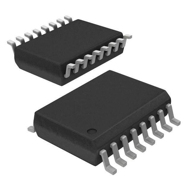
| 产品图片 |
|
| rohs | 符合RoHS无铅 / 符合限制有害物质指令(RoHS)规范要求 |
| 产品系列 | 接口 IC,数字隔离器,Texas Instruments ISO3080DW- |
| 数据手册 | |
| 产品型号 | ISO3080DW |
| PCN设计/规格 | |
| 上升/下降时间(典型值) | - |
| 产品目录页面 | |
| 产品种类 | |
| 传播延迟tpLH/tpHL(最大值) | - |
| 供应商器件封装 | 16-SOIC |
| 共模瞬态抗扰度(最小值) | 25kV/µs |
| 其它名称 | 296-23606-5 |
| 包装 | 管件 |
| 协议 | RS485 |
| 双工 | Full Duplex |
| 商标 | Texas Instruments |
| 安装类型 | 表面贴装 |
| 安装风格 | SMD/SMT |
| 封装 | Tube |
| 封装/外壳 | 16-SOIC(0.295",7.50mm 宽) |
| 封装/箱体 | SOIC-16 |
| 工作温度 | -40°C ~ 85°C |
| 工厂包装数量 | 40 |
| 技术 | 容性耦合 |
| 接收器滞后 | 30mV |
| 数据速率 | 200Kbps |
| 最大功率耗散 | 220 mW |
| 最大工作温度 | + 85 C |
| 最大数据速率 | 200 kb/s |
| 最小工作温度 | - 40 C |
| 标准包装 | 40 |
| 电压-电源 | 3.15 V ~ 5.5 V,4.5 V ~ 5.5 V |
| 电压-隔离 | 4000Vpk |
| 电源电压-最大 | 5.5 V |
| 电源电压-最小 | 3.15 V |
| 电源电流 | 8 mA, 15 mA |
| 类型 | RS422, RS485 |
| 系列 | ISO3080 |
| 绝缘电压 | 4 kVrms |
| 脉宽失真(最大) | 200ns, 200ns |
| 输入-输入侧1/输入侧2 | 2/1 |
| 输出类型 | Differential |
| 通道数 | 3 |
| 通道类型 | 单向 |
| 隔离式电源 | 是 |
| 驱动器/接收器数 | 1/1 |

.jpg)


- 商务部:美国ITC正式对集成电路等产品启动337调查
- 曝三星4nm工艺存在良率问题 高通将骁龙8 Gen1或转产台积电
- 太阳诱电将投资9.5亿元在常州建新厂生产MLCC 预计2023年完工
- 英特尔发布欧洲新工厂建设计划 深化IDM 2.0 战略
- 台积电先进制程称霸业界 有大客户加持明年业绩稳了
- 达到5530亿美元!SIA预计今年全球半导体销售额将创下新高
- 英特尔拟将自动驾驶子公司Mobileye上市 估值或超500亿美元
- 三星加码芯片和SET,合并消费电子和移动部门,撤换高东真等 CEO
- 三星电子宣布重大人事变动 还合并消费电子和移动部门
- 海关总署:前11个月进口集成电路产品价值2.52万亿元 增长14.8%


PDF Datasheet 数据手册内容提取
Product Order Technical Tools & Support & Reference Folder Now Documents Software Community Design ISO3080,ISO3082,ISO3086,ISO3088 SLOS581I–MAY2008–REVISEDAPRIL2017 ISO308x Isolated 5-V Full- and Half-Duplex RS-485 Transceivers 1 Features 3 Description • MeetsorExceedsTIA/EIARS-485Requirements The ISO3080 and ISO3086 devices are isolated full- 1 duplex differential line drivers and receivers while the • SignalingRatesupto20Mbps ISO3082 and ISO3088 devices are isolated half- • 1/8UnitLoad–Upto256NodesonaBus duplex differential line transceivers for TIA/EIA • ThermalShutdownProtection 485/422applications. • LowBusCapacitance– 16pF(Typical) These devices are ideal for long transmission lines • 50kV/μsTypicalTransientImmunity because the ground loop is broken to allow for a much larger common-mode voltage range. The • Fail-safeReceiverforBusOpen,Short,Idle symmetrical isolation barrier of the device is tested to • 3.3-VInputsare5-VTolerant provide 2500 V of isolation for 60 s per UL 1577 RMS • Bus-PinESDProtection between the bus-line transceiver and the logic-level interface. – 12-kVHBMBetweenBusPinsandGND2 – 6-kVHBMBetweenBusPinsandGND1 Any cabled I/O can be subjected to electrical noise transients from various sources. These noise • Safety-RelatedCertifications: transients can cause damage to the transceiver – 4000-VPKBasicInsulation,560VPKVIORMper and/or nearby sensitive circuitry if they are of DINVVDEV0884-10(VDEV0884-10): sufficient magnitude and duration. These isolated 2006-12andDINEN61010-1 devices can significantly increase protection and – 2500V IsolationperUL1577 reduce the risk of damage to expensive control RMS circuits. – 4000V IsolationperCSAComponent PK AcceptanceNotice5AandIEC60950-1 The ISO3080, ISO3082, ISO3086, and ISO3088 devicearequalifiedforusefrom–40°Cto+85°C. 2 Applications DeviceInformation(1) • SecuritySystems PARTNUMBER PACKAGE BODYSIZE(NOM) • ChemicalProduction ISO3080 • FactoryAutomation ISO3082 SOIC(16) 10.30mm×7.50mm • MotorandMotionControl ISO3086 • HVACandBuildingAutomationNetworks ISO3088 • NetworkedSecurityStations (1) For all available packages, see the orderable addendum at theendofthedatasheet. ISO3080,IOS3086FunctionDiagram ISO3082,IOS3088FunctionDiagram R 3 NATIO 14A DE 5 ATION RE 4 SOL 13B D 6 SOL DE 5 CI CI 13 D 6 GALVANI 1112YZ RRE 34 GALVANI 12AB 1 An IMPORTANT NOTICE at the end of this data sheet addresses availability, warranty, changes, use in safety-critical applications, intellectualpropertymattersandotherimportantdisclaimers.PRODUCTIONDATA.
ISO3080,ISO3082,ISO3086,ISO3088 SLOS581I–MAY2008–REVISEDAPRIL2017 www.ti.com Table of Contents 1 Features.................................................................. 1 8 DetailedDescription............................................ 17 2 Applications........................................................... 1 8.1 Overview.................................................................17 3 Description............................................................. 1 8.2 FunctionalBlockDiagrams.....................................17 4 RevisionHistory..................................................... 2 8.3 FeatureDescription.................................................18 8.4 DeviceFunctionalModes........................................18 5 PinConfigurationandFunctions......................... 4 9 ApplicationandImplementation........................ 20 6 Specifications......................................................... 5 9.1 ApplicationInformation............................................20 6.1 AbsoluteMaximumRatings .....................................5 9.2 TypicalApplication .................................................20 6.2 ESDRatings..............................................................5 10 PowerSupplyRecommendations..................... 22 6.3 RecommendedOperatingConditions.......................5 6.4 ThermalInformation..................................................6 11 Layout................................................................... 22 6.5 InsulationSpecifications............................................6 11.1 LayoutGuidelines.................................................22 6.6 Safety-RelatedCertifications.....................................6 11.2 LayoutExample....................................................23 6.7 SafetyLimitingValues..............................................7 12 DeviceandDocumentationSupport................. 24 6.8 ElectricalCharacteristics:Driver...............................7 12.1 DocumentationSupport........................................24 6.9 ElectricalCharacteristics:Receiver..........................8 12.2 RelatedLinks........................................................24 6.10 SupplyCurrent........................................................9 12.3 ReceivingNotificationofDocumentationUpdates24 6.11 SwitchingCharacteristics:Driver............................9 12.4 CommunityResources..........................................24 6.12 SwitchingCharacteristics:Receiver........................9 12.5 Trademarks...........................................................24 6.13 InsulationCharacteristicsCurves.........................10 12.6 ElectrostaticDischargeCaution............................24 6.14 TypicalCharacteristics..........................................11 12.7 Glossary................................................................25 7 ParameterMeasurementInformation................13 13 Mechanical,Packaging,andOrderable Information........................................................... 25 4 Revision History NOTE:Pagenumbersforpreviousrevisionsmaydifferfrompagenumbersinthecurrentversion. ChangesfromRevisionH(December2015)toRevisionI Page • ChangedtheL(I01)andL(I02)parameterstoexternalclearanceandexternalcreepage,respectively............................... 6 • ChangedtheV parametertoapparentcharge .................................................................................................................. 6 PR • SwitchedtheRandDpinsofthemasterdeviceintheTypicalRS-485NetworkWithFull-DuplexTransceiversfigure....20 • AddedtheReceivingNotificationofDocumentationUpdatessection................................................................................. 24 • ChangedtheElectrostaticDischargeCautionstatement .................................................................................................... 24 ChangesfromRevisionG(July2015)toRevisionH Page • ChangedtheCDMvalueinESDRatingsFrom:±200To:±1000 ......................................................................................... 5 • ChangedtheMONvalueofL(IO1)inInsulationandSafety-RelatedPackageCharacteristicsFrom:8.34To:8mm ........6 • ChangedtheMONvalueofL(IO2)inInsulationandSafety-RelatedPackageCharacteristicsFrom:8.1To:8mm ..........6 • Movedthelastlistitem"Routingthehigh-speedtraces..."tothesecondlistitemsinLayoutGuidelinessection.............22 ChangesfromRevisionF(May2015)toRevisionG Page • Deleted"Ratedmainsvoltage≤400V "fromIEC60664-1RatingsTable....................................................................... 6 RMS • Changed"Maximumcasetemperature"To:"Maximumsafetytemperature"inSafetyLimiting............................................ 7 • ChangedtheLayoutGuidelinessection.............................................................................................................................. 22 2 SubmitDocumentationFeedback Copyright©2008–2017,TexasInstrumentsIncorporated ProductFolderLinks:ISO3080 ISO3082 ISO3086 ISO3088
ISO3080,ISO3082,ISO3086,ISO3088 www.ti.com SLOS581I–MAY2008–REVISEDAPRIL2017 ChangesfromRevisionE(September2011)toRevisionF Page • AddedESDRatingtable,ThermalInformationtable,FeatureDescriptionsection,DeviceFunctionalModes, ApplicationandImplementationsection,PowerSupplyRecommendationssection,Layoutsection,Deviceand DocumentationSupportsection,andMechanical,Packaging,andOrderableInformationsection....................................... 1 • ChangedFeatureslistitemFrom:IEC60747-5-2(VDE0884,Rev.2)To:DINVVDEV0884-10(VDEV0884-10): 2006-12................................................................................................................................................................................... 1 • VDEstandardchangedtoDINVVDEV0884-10(VDEV0884-10):2006-12....................................................................... 1 • ChangedIEC60664-1RatingsTable.BasicisolationgroupSPECIFICATIONentryFrom:IIIaTo:II................................. 6 ChangesfromRevisionD(January2011)toRevisionE Page • ChangedFeatureslistitemFrom:16kVHBMTo:12kVHBM............................................................................................. 1 • ChangedESDHBMspecvaluefrom±16to±12inESDRatings......................................................................................... 5 ChangesfromRevisionC(October2009)toRevisionD Page • AddedT rowtotheAbsoluteMaximumRatings............................................................................................................... 5 STG • Added"Dynamic"conditionstoRecommendedOperatingConditionsV specwithreferencetoISO3086 ID RecommendedMinimumDifferentialInputVoltagevsSignalingRate.................................................................................. 5 • Changedfor3Vto3.3Vinnote1oftheRecommendedOperatingConditionstable......................................................... 5 • ChangedFileNumberfrom'1698195'to'220991inRegulatoryInformation ....................................................................... 6 • Changedθ from212°C/Wto168°C/WinconditionsstatementforI spec.;andMAXcurrentfrom210mAto JA S 157mAinSafetyLimiting....................................................................................................................................................... 7 • DeletedV =V or0VfromCMTIspec.Conditionsstatement.Added"Figure13"inElectricalCharacteristics:Driver...7 I CCI • Changedtoprow,UNITcolumn,splitinto2rows,toprowµsandsecondrownsinSwitchingCharacteristics:Driver.......9 • Changedgraphfor"DW-16θ ThermalDeratingCurveperIEC60747-5-2",ThermalDeratingCurve.........................10 JC • AddedtheISO3086RecommendedMinimumDifferentialInputVoltagevsSignalingRategraph..................................... 11 • AddednotetobottomoffirstpageoftheParameterMeasurementInformation................................................................. 13 • AddedFootnotestotheDriverFunctionTableandReceiverFunctionTable..................................................................... 18 ChangesfromRevisionB(December2008)toRevisionC Page • ChangedRecommendedOperatingConditionstablenoteFrom:For3-Voperation,V orV isspecifiedfrom CC1 CC2 3.15Vto3.6V.To:For3-Voperation,V isspecifiedfrom3.15Vto3.6V........................................................................ 5 CC1 ChangesfromRevisionA(June2008)toRevisionB Page • ChangedFeaturesbulletFrom:4000-V Isolation,To:4000-V Isolation,,560-V V ...................................... 1 PEAK PEAK PEAK IORM • AddedtheCSAcolumntoRegulatoryInformation................................................................................................................. 6 ChangesfromOriginal(May2008)toRevisionA Page • DeletedtheCSAcolumnfromRegulatoryInformation.......................................................................................................... 6 • ChangedthefilenumberintheVDEcolumninRegulatoryInformationFrom:40014131To:40016131............................. 6 Copyright©2008–2017,TexasInstrumentsIncorporated SubmitDocumentationFeedback 3 ProductFolderLinks:ISO3080 ISO3082 ISO3086 ISO3088
ISO3080,ISO3082,ISO3086,ISO3088 SLOS581I–MAY2008–REVISEDAPRIL2017 www.ti.com 5 Pin Configuration and Functions ISO3080andISO3086DWPackage ISO3082andISO3088DWPackage 16-PinSOIC 16-PinSOIC TopView TopView V 1 16 V V 1 16 V CC1 CC2 CC1 CC2 GND1 2 15 GND2 GND1 2 15 GND2 R 3 14 A R 3 14 NC RE 4 13 B RE 4 13 B DE 5 12 Z DE 5 12 A D 6 11 Y D 6 11 NC GND1 7 10 GND2 GND1 7 10 GND2 GND1 8 9 GND2 GND1 8 9 GND2 PinFunctions PIN ISO3080, ISO3082, I/O DESCRIPTION NAME ISO3086 ISO3088 14 — I Receivernoninvertinginputonthebus-side A — 12 I/O TransceivernoninvertingInputoroutput(I/O)onthebus-side 13 — I ReceiverinvertingInputonthebus-side B — 13 I/O Transceiverinvertinginputoroutput(I/O)onthebus-side D 6 6 I Driverinput DE 5 5 I Enables(whenhigh)ordisables(whenloworopen)driveroutputofISO308x 2 2 GND1 7 7 — GroundconnectionforV CC1 8 8 9 9 GND2 10 10 — GroundconnectionforV CC2 15 15 11 NC — — Noconnect 14 R 3 3 O Receiveroutput RE 4 4 I Disables(whenhighoropen)orenables(whenlow)receiveroutputofISO308x V 1 1 — Powersupply,V CC1 CC1 V 16 16 — Powersupply,V CC2 CC2 Y 11 — O Drivernoninvertingoutput Z 12 — O Driverinvertingoutput 4 SubmitDocumentationFeedback Copyright©2008–2017,TexasInstrumentsIncorporated ProductFolderLinks:ISO3080 ISO3082 ISO3086 ISO3088
ISO3080,ISO3082,ISO3086,ISO3088 www.ti.com SLOS581I–MAY2008–REVISEDAPRIL2017 6 Specifications 6.1 Absolute Maximum Ratings See (1). MIN MAX UNIT VCC Inputsupplyvoltage(2) VCC1,VCC2 –0.3 6 V VO VoltageatanybusI/Opin –9 14 V VIT Voltageinput,transientpulse(through100Ω,seeFigure21) A,B,Y,andZ –50 50 V VI VoltageinputatanyD,DEorREpin –0.5 7 V IO Receiveroutputcurrent ±10 mA TJ Maximumjunctiontemperature 150 °C Tstg Storagetemperature –65 150 °C (1) Stressesbeyondthoselistedunderabsolutemaximumratingsmaycausepermanentdamagetothedevice.Thesearestressratings onlyandfunctionaloperationofthedeviceattheseoranyotherconditionsbeyondthoseindicatedunderrecommendedoperating conditionsisnotimplied.Exposuretoabsolute-maximum-ratedconditionsforextendedperiodsmayaffectdevicereliability. (2) AllvoltagevaluesexceptdifferentialI/Obusvoltagesarewithrespecttonetworkgroundterminalandarepeakvoltagevalues. 6.2 ESD Ratings VALUE UNIT BuspinsandGND1 ±6000 Electrostatic Humanbodymodel(HBM),perANSI/ESDA/JEDECJS-001(1) BuspinsandGND2 ±12000 V(ESD) discharge Allpins ±4000 V Chargeddevicemodel(CDM),perJEDECspecificationJESD22-C101(2) ±1000 (1) JEDECdocumentJEP155statesthat500-VHBMallowssafemanufacturingwithastandardESDcontrolprocess. (2) JEDECdocumentJEP157statesthat250-VCDMallowssafemanufacturingwithastandardESDcontrolprocess. 6.3 Recommended Operating Conditions MIN TYP MAX UNIT VCC1 Logic-sidesupplyvoltage(1) 3.15 5.5 V VCC2 Bus-sidesupplyvoltage(1) 4.5 5 5.5 V VOC VoltageateitherbusI/Opin A,B –7 12 V VIH High-levelinputvoltage D,DE,RE 2 VCC V VIL Low-levelinputvoltage D,DE,RE 0 0.8 AwithrespecttoB –12 12 VID Differentialinputvoltage V Dynamic(ISO3086) SeeFigure10 RL Differentialinputresistance 54 60 Ω Driver –60 60 IO Outputcurrent mA Receiver –8 8 TA Ambienttemperature –40 85 °C (1) For5-Voperation,V orV isspecifiedfrom4.5Vto5.5V.For3.3-Voperation,V isspecifiedfrom3.15Vto3.6V. CC1 CC2 CC1 Copyright©2008–2017,TexasInstrumentsIncorporated SubmitDocumentationFeedback 5 ProductFolderLinks:ISO3080 ISO3082 ISO3086 ISO3088
ISO3080,ISO3082,ISO3086,ISO3088 SLOS581I–MAY2008–REVISEDAPRIL2017 www.ti.com 6.4 Thermal Information ISO308x THERMALMETRIC(1) DW(SOIC) UNIT 16PINS Low-Kthermalresistance(2) 168 RθJA Junction-to-ambientthermalresistance °C/W High-Kthermalresistance 79.6 RθJC(top) Junction-to-case(top)thermalresistance 39.7 °C/W RθJB Junction-to-boardthermalresistance 44.7 °C/W ψJT Junction-to-topcharacterizationparameter 11.8 °C/W ψJB Junction-to-boardcharacterizationparameter 44.0 °C/W RθJC(bot) Junction-to-case(bottom)thermalresistance — °C/W (1) Formoreinformationabouttraditionalandnewthermalmetrics,seetheSemiconductorandICPackageThermalMetricsapplication report. (2) TestedinaccordancewiththeLow-KorHigh-KthermalmetricdefinitionsofEIA/JESD51-3forleadedsurfacemountpackages. 6.5 Insulation Specifications PARAMETER TESTCONDITIONS VALUE UNIT GENERAL CLR Externalclearance(1) Shortestterminal-to-terminaldistancethroughair 8 mm CPG Externalcreepage(1) Shortestterminal-to-terminaldistanceacrossthe 8 mm packagesurface DTI Distancethroughtheinsulation Minimuminternalgap(internalclearance) 0.008 mm CTI Comparativetrackingindex DINEN60112(VDE0303-11) ≥400 V Materialgroup II Ratedmainsvoltage≤150V I-IV RMS Overvoltagecategory Ratedmainsvoltage≤300V I-III RMS DINVVDEV0884-10(VDEV0884-10):2006-12(2) V Maximumrepetitivepeakisolationvoltage ACvoltage(bipolar) 560 V IORM PK V =V ,t=60s(qualification); V Maximumtransientisolationvoltage TEST IOTM 4000 V IOTM t=1s(100%production) PK Methodb1,V =V ×1.5, q Apparentcharge(3) PR IORM ≤5 pC pd 100%Productiontestwitht=1s C Barriercapacitance,inputtooutput(4) V =0.4sin(4E6πt) 2 pF IO I VIO=500V,TA=25°C,allpinsoneachsideofthe >1012 Ω R Isolationresistance,inputtooutput(4) barriertiedtogethercreatinga2-terminaldevice IO V =500VatT =150°C >109 Ω IO S Pollutiondegree 2 Climaticcategory 40/125/21 (1) Creepageandclearancerequirementsshouldbeappliedaccordingtothespecificequipmentisolationstandardsofanapplication.Care shouldbetakentomaintainthecreepageandclearancedistanceofaboarddesigntoensurethatthemountingpadsoftheisolatoron theprinted-circuitboarddonotreducethisdistance.Creepageandclearanceonaprinted-circuitboardbecomeequalincertaincases. Techniquessuchasinsertinggroovesand/orribsonaprintedcircuitboardareusedtohelpincreasethesespecifications. (2) Thiscouplerissuitableforbasicelectricalinsulationonlywithinthemaximumoperatingratings.Compliancewiththesafetyratingsshall beensuredbymeansofsuitableprotectivecircuits. (3) Apparentchargeiselectricaldischargecausedbyapartialdischarge(pd). (4) Allpinsoneachsideofthebarriertiedtogethercreatingatwo-terminaldevice 6.6 Safety-Related Certifications VDE CSA UL CertifiedaccordingtoDINVVDEV0884-10(VDE ApprovedunderCSAComponent RecognizedunderUL1577 V0884-10):2006-12 AcceptanceNotice5AandIEC60950-1 ComponentRecognitionProgram Basicinsulation, 4000V Isolationrating, PK 4000VPKMaximumtransientovervoltage, 560VPKBasicworkingvoltageperCSA SingleProtection,2500VRMS 560V Maximumrepetitivepeakisolationvoltage 60950-1-07andIEC60950-1(2ndEd) PK Certificatenumber:40016131 Mastercontractnumber:220991 Filenumber:E181974 6 SubmitDocumentationFeedback Copyright©2008–2017,TexasInstrumentsIncorporated ProductFolderLinks:ISO3080 ISO3082 ISO3086 ISO3088
ISO3080,ISO3082,ISO3086,ISO3088 www.ti.com SLOS581I–MAY2008–REVISEDAPRIL2017 6.7 Safety Limiting Values Safetylimiting(1)intendstominimizepotentialdamagetotheisolationbarrieruponfailureofinputoroutputcircuitry.Afailure oftheI/Ocanallowlowresistancetogroundorthesupplyand,withoutcurrentlimiting,dissipatesufficientpowertooverheat thedieanddamagetheisolationbarrier,potentiallyleadingtosecondarysystemfailures. PARAMETER TESTCONDITIONS MIN TYP MAX UNIT Safetyinput,output,orsupply R =79.6°C/W,V =5.5V,T =150°C,T =25°C, I θJA I J A 286 mA S current seeFigure1 T Safetytemperature 150 °C S (1) Thesafety-limitingconstraintisthemaximumjunctiontemperaturespecifiedinthedatasheet.Thepowerdissipationandjunction-to-air thermalimpedanceofthedeviceinstalledintheapplicationhardwaredeterminesthejunctiontemperature.Theassumedjunction-to-air thermalresistanceintheThermalInformationtableisthatofadeviceinstalledonahigh-Ktestboardforleadedsurface-mount packages.Thepoweristherecommendedmaximuminputvoltagetimesthecurrent.Thejunctiontemperatureisthentheambient temperatureplusthepowertimesthejunction-to-airthermalresistance. 6.8 Electrical Characteristics: Driver overrecommendedoperatingconditions(unlessotherwisenoted) PARAMETER TESTCONDITIONS MIN TYP MAX UNIT I =0mA,noload 3 4.3 V O CC Differentialoutputvoltage RL=54Ω,SeeFigure11 1.5 2.3 |V | V OD magnitude R =100Ω(RS-422),SeeFigure11 2 2.3 L V from–7Vto+12V,SeeFigure12 1.5 test Changeinmagnitudeofthe Δ|V | SeeFigure11andFigure12 –0.2 0 0.2 V OD differentialoutputvoltage Steady-statecommon-mode V SeeFigure13 1 2.6 3 OC(SS) outputvoltage V Changeinsteady-statecommon- ΔV SeeFigure13 –0.1 0.1 OC(SS) modeoutputvoltage Peak-to-peakcommon-mode V SeeFigure13 0.5 V OC(pp) outputvoltage I Inputcurrent D,DE,V at0VorV –10 10 μA I I CC1 Seethereceiverbiasinput ISO3082,ISO3088 currentparameter V orV =12V, Y Z High-impedancestateoutput V =0Vor5V, 1 I CC OZ current ISO3080 DE=0V,Otherinputat0V μA ISO3086 V orV =–7V. Y Z V =0Vor5V, –1 CC DE=0V,Otherinputat0V V orV at–7V,Otherinputat0V A B I Short-circuitoutputcurrent –200 200 mA OS V orV at12V,Otherinputat0V A B Common-modetransient CMTI SeeFigure22andFigure23 25 50 kV/μs immunity Copyright©2008–2017,TexasInstrumentsIncorporated SubmitDocumentationFeedback 7 ProductFolderLinks:ISO3080 ISO3082 ISO3086 ISO3088
ISO3080,ISO3082,ISO3086,ISO3088 SLOS581I–MAY2008–REVISEDAPRIL2017 www.ti.com 6.9 Electrical Characteristics: Receiver overrecommendedoperatingconditions(unlessotherwisenoted) PARAMETER TESTCONDITIONS MIN TYP MAX UNIT Positive-goinginputthreshold V I =–8mA –85 –10 mV IT(+) voltage O Negative-goinginputthreshold V I =8mA –200 –115 mV IT(–) voltage O V Hysteresisvoltage(V –V ) 30 mV hys IT+ IT– V – V High-leveloutputvoltage VID=200mV,IO=–8mA, 3.3-VVCC1 CC01.4 3.1 V OH SeeFigure17 5-VV 4 4.8 CC1 V Low-leveloutputvoltage VID=–200mV,IO=8mA, 3.3-VVCC1 0.15 0.4 V OL SeeFigure17 5-VV 0.15 0.4 CC1 High-impedancestateoutput I V =–7to12V,Otherinput=0V –1 1 μA O(Z) current I V orV =12V,Otherinputat0V 0.04 0.1 A B V orV =12V,V =0,Otherinputat0V 0.06 0.13 A B CC I Businputcurrent mA I V orV =–7V,Otherinputat0V –0.1 –0.04 A B V orV =–7V,V =0,Otherinputat0V –0.05 –0.03 A B CC I High-levelinputcurrent,RE V =2V –10 10 μA IH IH I Low-levelinputcurrent,RE V =0.8V –10 10 μA IL IL R Differentialinputresistance A,B 48 kΩ ID Testinputsignalisa1.5-MHzsinewavewith C Differentialinputcapacitance 1-V amplitude.C ismeasuredacrossA 7 pF D PP D andB C Inputcapacitancetoground VI=0.4sin(4E6πt) 2 pF I 8 SubmitDocumentationFeedback Copyright©2008–2017,TexasInstrumentsIncorporated ProductFolderLinks:ISO3080 ISO3082 ISO3086 ISO3088
ISO3080,ISO3082,ISO3086,ISO3088 www.ti.com SLOS581I–MAY2008–REVISEDAPRIL2017 6.10 Supply Current overrecommendedoperatingcondition(unlessotherwisenoted) PARAMETER TESTCONDITIONS MIN TYP MAX UNIT REat0VorV ,DEat0V CC 3.3-VV 8 orV CC1 CC1 I Logic-sidesupplycurrent mA CC1 REat0VorV ,DEat0V CC 5-VV 10 orV CC1 CC1 I Bus-sidesupplycurrent REat0VorV ,DEat0V,Noload 15 mA CC2 CC 6.11 Switching Characteristics: Driver overrecommendedoperatingconditions(unlessotherwisenoted) PARAMETER TESTCONDITIONS MIN TYP MAX UNIT ISO3080/82 0.7 1.3 μs t ,t Propagationdelay PLH PHL ISO3086/88 25 45 ns PWD(1) PtPuLHls|e) skew(|tPHL– IISSOO33008806//8828 SeeFigure14 203 270.50 ns Differentialoutput ISO3080/82 0.5 0.9 1.5 μs t,t signalriseandfall r f time ISO3086/88 7 15 ns Propagationdelay, SeeFigure15and 50%V 2.5 7 O high-impedance-to- ISO3080/82 Figure16, μs tPZH, high-leveloutputand DEat0V 90%VO 1.8 t PZL high-impedance-to- low-leveloutput ISO3086/88 25 55 ns Propagationdelay, ISO3080/82 95 225 high-level-to-high- SeeFigure15andFigure16,DEat0V t , PHZ impedanceoutput ns tPLZ andlow-leveltohigh- ISO3086/88 25 55 impedanceoutput (1) Alsoknownaspulseskew 6.12 Switching Characteristics: Receiver overrecommendedoperatingconditions(unlessotherwisenoted) PARAMETER TESTCONDITIONS MIN TYP MAX UNIT t ,t Propagationdelay 90 125 PLH PHL ns PWD(1) Pulsewidthdistortion|t –t | SeeFigure18 4 12 PHL PLH t,t Outputsignalriseandfalltime 1 ns r f Propagationdelay,high-level-to- t , PHZ high-impedanceoutputandhigh- SeeFigure19,DEat0V 22 ns t PZH impedance-to-high-leveloutput Propagationdelay,high- tPZL, impedance-to-low-leveloutput SeeFigure20,DEat0V 22 ns t andlow-level-to-high-impedance PLZ output (1) Alsoknownaspulseskew. Copyright©2008–2017,TexasInstrumentsIncorporated SubmitDocumentationFeedback 9 ProductFolderLinks:ISO3080 ISO3082 ISO3086 ISO3088
ISO3080,ISO3082,ISO3086,ISO3088 SLOS581I–MAY2008–REVISEDAPRIL2017 www.ti.com 6.13 Insulation Characteristics Curves 300 VCC1 = VCC2 =5.5 V A) m ( nt 200 e urr C g n miti Li 100 y et af S 0 0 50 100 150 200 CaseTemperature (°C) D001 Figure1.ThermalDeratingCurveforLimitingCurrentperVDE 10 SubmitDocumentationFeedback Copyright©2008–2017,TexasInstrumentsIncorporated ProductFolderLinks:ISO3080 ISO3082 ISO3086 ISO3088
ISO3080,ISO3082,ISO3086,ISO3088 www.ti.com SLOS581I–MAY2008–REVISEDAPRIL2017 6.14 Typical Characteristics 60 30 50 25 A) A) m 40 m 20 nt ( nt ( Curre 30 IICCCC12((35. 3V )V) Curre 15 IICCCC12((35. 3V )V) y y pl pl p 20 p 10 u u S S 10 5 0 0 0 50 100 150 200 0 50 100 150 200 Data Rate (kbps) Data Rate (kbps) D002 D003 Figure2.ISO3080SupplyCurrentvsDataRateWithLoad Figure3.ISO3080SupplyCurrentvsDataRateWithNo Load 60 50 I (3.3 V) CC1 I (5 V) 50 CC2 40 A) A) m 40 m nt ( nt ( 30 Curre 30 IICCCC12((35. 3V )V) Curre y y 20 pl pl p 20 p u u S S 10 10 0 0 0 50 100 150 200 0 50 100 150 200 Data Rate (kbps) Data Rate (kbps) D004 D005 Figure4.ISO3082SupplyCurrentvsDataRateWithLoad Figure5.ISO3082SupplyCurrentvsDataRateWithNo Load 80 70 I (3.3 V) CC1 70 60 ICC2(5 V) 60 A) A) 50 m m nt ( 50 nt ( 40 y Curre 40 IICCCC12((35. 3V )V) y Curre 30 pl 30 pl p p Su Su 20 20 10 10 0 0 0 5 10 15 20 0 5 10 15 20 Data Rate (Mbps) Data Rate (Mbps) D007 D006 Figure6.ISO3086SupplyCurrentvsDataRateWithLoad Figure7.ISO3086SupplyCurrentvsDataRateWithNo Load Copyright©2008–2017,TexasInstrumentsIncorporated SubmitDocumentationFeedback 11 ProductFolderLinks:ISO3080 ISO3082 ISO3086 ISO3088
ISO3080,ISO3082,ISO3086,ISO3088 SLOS581I–MAY2008–REVISEDAPRIL2017 www.ti.com Typical Characteristics (continued) 80 70 I (3.3 V) CC1 70 60 ICC2(5 V) 60 A) A) 50 m m nt ( 50 nt ( 40 y Curre 40 IICCCC12((35. 3V )V) y Curre 30 pl 30 pl p p Su Su 20 20 10 10 0 0 0 5 10 15 20 0 5 10 15 20 Data Rate (Mbps) Data Rate (Mbps) D008 D009 Figure8.ISO3088SupplyCurrentvsDataRateWithLoad Figure9.ISO3088SupplyCurrentvsDataRateWithNo Load 1 0.9 0.8 k p e - 0.7 g a olt 0.6 V ut p 0.5 n al I nti 0.4 e Differ 0.3 - D0.2 VI 0.1 0 0 2 4 6 8 10 12 14 16 18 20 Signaling Rate - Mbps Figure10.ISO3086RecommendedMinimumDifferentialInputVoltagevsSignalingRate 12 SubmitDocumentationFeedback Copyright©2008–2017,TexasInstrumentsIncorporated ProductFolderLinks:ISO3080 ISO3082 ISO3086 ISO3088
ISO3080,ISO3082,ISO3086,ISO3088 www.ti.com SLOS581I–MAY2008–REVISEDAPRIL2017 7 Parameter Measurement Information V V CC1 CC2 DE IOA A DE 375W A V0CoCr1 II B VOD 0 V or 3 V D B VO+–D 60W –7 V to 12 V GND 1 GND 2 IOB VI GND 2 375W VOB VOA GND 1 GND 2 Figure11.DriverV TestandCurrentDefinitions Figure12.DriverV WithCommon-ModeLoading OD OD TestCircuit NOTE Unless otherwise stated, test circuits are shown for half-duplex devices, ISO3082 and ISO3088.Forfull-duplexdevices,thedriveroutputpinsareYandZ. V CC1 DE IOA 27W A A VA Input II VOD B B VB 27W GND1 GND2 IOB VI VOC VOC(p-p) VOC(SS) VOB VOA VOC GND1 GND2 InputGenerator:PRR=100kHz,50%duty cycle,tr<6ns,tf<6ns,ZO=50W Figure13. TestCircuitandWaveformDefinitionsForTheDriverCommon-ModeOutputVoltage V DE 3 V CC1 A VOD 50% 50% D RL= 54W CL= 50 pF VI GeInnepruattor VI 50W B ±1% ±20% tPLH tPHL VOD(H) 90% 90% Generator: PRR=100kHz,G50N%Dd 1utycycle, instruCmLeinntcalutiodne sc afixptaucrieta anncde VOD 10%50% 501%0% tr<6ns,tf <6ns,ZO=50 tr tf VOD(L) Figure14. DriverSwitchingTestCircuitandVoltageWaveforms Copyright©2008–2017,TexasInstrumentsIncorporated SubmitDocumentationFeedback 13 ProductFolderLinks:ISO3080 ISO3082 ISO3086 ISO3088
ISO3080,ISO3082,ISO3086,ISO3088 SLOS581I–MAY2008–REVISEDAPRIL2017 www.ti.com Parameter Measurement Information (continued) 3V 3V if testingAout,put A S1 0V if testing B output VO VI 50% 50% 3 V or 0 V D 0V t PZH DE R = 110W VOH L 90% ±1% Input CL= 50 pF ±20% VO 50% Generator VI 50W CLincludes fixture and t ~~0 V instrumentation PHZ capacitance GND 1 Generator PRR = 50 kHz, 50% duty cycle, t <6ns, t <6ns, Z = 50W r f O Figure15. DriverHigh-LevelOutputEnableandDisableTimeTestCircuitandVoltageWaveforms 3V R = 110W 03VV iiff tteessttiinngg AB oouuttpp,uutt A S1 ±1L% 3V D 50% 50% 3V or0V VI 0 V B DE tPZL tPLZ 5V Input CL= 50 pF ±20% VO 50% Generator VI 50W CLiinncslturudmese fnixtatutiroen and 10% VOL capacitance GND2 Generator:PRR=50kHz,50%dutycycle, tr<6ns,tf<6ns,Z =50 Figure16. DriverLow-LevelOutputEnableandDisableTimeTestCircuitandVoltageWaveform IA A IO R VA VID B VIC VO VA+VB VB IB 2 Figure17. ReceiverVoltageandCurrentDefinitions 3 V A 50% 50% Input R VO VI Generator VI 50W 0 V C = 15 pF 1.5V B RE ±2L0% tPLH tPHL 90% VOH Generator:PtRrR<=61n0s0,tkfH<z,65n0s%,ZOdu=ty5c0ycWle, insCtrLuminecnlutadteiosn f icxatupraec aitnadnce VO 50% 501%0% V t t OL r f Figure18. ReceiverSwitchingTestCircuitandWaveforms 14 SubmitDocumentationFeedback Copyright©2008–2017,TexasInstrumentsIncorporated ProductFolderLinks:ISO3080 ISO3082 ISO3086 ISO3088
ISO3080,ISO3082,ISO3086,ISO3088 www.ti.com SLOS581I–MAY2008–REVISEDAPRIL2017 Parameter Measurement Information (continued) VCC A 1.5V R VO 1 kW ±1% 3V S1 VI 50% 50% 0V B CL=15pF±20% RE aCnLd inincslutrduemse fnixtatutiroen tPZH tpHZ capacitance VOH 90% Input VO 50% Generator VI 50W !0V Generator:PRR=100kHz,50%dutycycle, tr<6ns,tf<6ns,ZO=50W Figure19. ReceiverEnableTestCircuitandWaveforms,DataOutputHigh VCC A 3V 0V R VO 1 kW±1% VI S1 50% 50% 1.5V B CL=15pF±20% 0V RE aCnLd inincslutrduemse fnixtatutiroen tPZL tPLZ capacitance V CC Input V 50% Generator VI 50W O 10% VOL Generator:PRR=100kHz,50%dutycycle, tr<6ns,tf<6ns,ZO=50W Figure20. ReceiverEnableTestCircuitandWaveforms,DataOutputLow 0V A RE R B 100W±1% Pulse Generator 15ms duration + 1% duty cycle _ D tr, tf£100 ns DE 3V Note:This test is conducted to test survivability only. Data stability at the R output is not specified. Figure21. TransientOvervoltageTestCircuit Copyright©2008–2017,TexasInstrumentsIncorporated SubmitDocumentationFeedback 15 ProductFolderLinks:ISO3080 ISO3082 ISO3086 ISO3088
ISO3080,ISO3082,ISO3086,ISO3088 SLOS581I–MAY2008–REVISEDAPRIL2017 www.ti.com Parameter Measurement Information (continued) 2 V C = 0.1mF VCC1 VCC2 ±1% A C = 0.1mF±1% DE GND1 D S1 54W V or V OH OL B 0.8 V R RE VOHor VOL 1 kW GND1 GND2 CL= 15 pF (includes probe and jig capacitance) VTEST Figure22. Half-DuplexCommon-ModeTransientImmunityTestCircuit C = 0.1mF VCC1 VCC2 2 V ±1% Y C = 0.1mF±1% DE GND1 D S1 54W VOHor VOL Z A 0.8 V 1.5V or0V 54W RE VOHor VOL 1 kW B 0V or1.5V GND1 GND2 CL= 15 pF (includes probe and jig capacitance) VTEST Figure23. Full-DuplexCommon-ModeTransientImmunityTestCircuit 16 SubmitDocumentationFeedback Copyright©2008–2017,TexasInstrumentsIncorporated ProductFolderLinks:ISO3080 ISO3082 ISO3086 ISO3088
ISO3080,ISO3082,ISO3086,ISO3088 www.ti.com SLOS581I–MAY2008–REVISEDAPRIL2017 8 Detailed Description 8.1 Overview The ISO3080 and ISO3086 devices are isolated full-duplex differential line drivers and receivers while the ISO3082 and ISO3088 devices are isolated half-duplex differential line transceivers for TIA/EIA 485/422 applications. They are rated to provide galvanic isolation of up to 2500 V for 60 s as per the standard. They RMS have active-high driver enables and active-low receiver enables to control the data flow. They are available in twospeedgradessuitablefordatatransmissionupto200kbpsand20Mbps. When the driver enable pin, DE, is logic high, the differential outputs Y and Z follow the logic states at data input D. A logic high at D causes Y to turn high and Z to turn low. In this case the differential output voltage defined as V = V – V is positive. When D is low, the output states reverse, Z turns high, Y becomes low, and V is OD (Y) (Z) OD negative. When DE is low, both outputs turn high-impedance. In this condition the logic state at D is irrelevant. The DE pin has an internal pulldown resistor to ground, thus when left open the driver is disabled (high- impedance) by default. The D pin has an internal pullup resistor to V , thus, when left open while the driver is CC enabled,outputYturnshighandZturnslow. When the receiver enable pin, RE, is logic low, the receiver is enabled. When the differential input voltage defined as V = V – V is positive and higher than the positive input threshold, V , the receiver output, R, ID (A) (B) IT+ turns high. When V is negative and less than the negative and lower than the negative input threshold, V , ID IT– the receiver output, R, turns low. If V is between V and V the output is indeterminate. When RE is logic ID IT+ IT– high or left open, the receiver output is high-impedance and the magnitude and polarity of V are irrelevant. ID Internal biasing of the receiver inputs causes the output to go failsafe-high when the transceiver is disconnected fromthebus(open-circuit),thebuslinesareshorted(short-circuit),orthebusisnotactivelydriven(idlebus). 8.2 Functional Block Diagrams N O 14 R 3 ATI A 4 OL 13 RE S B 5 I DE C ANI 12Z 6 V D GAL 11Y Figure24. ISO3080,IOS3086FunctionalDiagram DE 5 TION A L 6 O D S I C 13 3 NI B R A 12 4 LV A RE A G Figure25. ISO3082,IOS3088FunctionalDiagram Copyright©2008–2017,TexasInstrumentsIncorporated SubmitDocumentationFeedback 17 ProductFolderLinks:ISO3080 ISO3082 ISO3086 ISO3088
ISO3080,ISO3082,ISO3086,ISO3088 SLOS581I–MAY2008–REVISEDAPRIL2017 www.ti.com 8.3 Feature Description Table1providesanoverviewofthedevicefeatures. Table1.DeviceFeatures DEVICE RATEDISOLATION(1) TYPE DATARATE ISO3080 4000V /2500V Full-duplex 200kbps PK RMS ISO3086 4000V /2500V Full-duplex 20Mbps PK RMS ISO3082 4000V /2500V Half-duplex 200kbps PK RMS ISO3088 4000V /2500V Half-duplex 20Mbps PK RMS (1) SeeSafety-RelatedCertificationstablefordetailedisolationratings. 8.4 Device Functional Modes Table2liststhedriverfunctionalmodesandTable3 liststhereceiverfunctionalmodes. Table2.DriverFunctionTable(1) INPUT ENABLEINPUT OUTPUTS(2) V V CC1 CC2 (D) (DE) Y/A Z/B PU PU H H H L PU PU L H L H PU PU X L Hi-Z Hi-Z PU PU X OPEN Hi-Z Hi-Z PU PU OPEN H H L PD PU X X Hi-Z Hi-Z PU PD X X Hi-Z Hi-Z PD PD X X Hi-Z Hi-Z (1) PU=PoweredUp;PD=PoweredDown;H=LogicHigh;L=LogicLow;X=Irrelevant,Hi-Z=HighImpedance(off) (2) DriveroutputpinsareYandZforfull-duplexdevicesandAandBforhalf-duplexdevices. Table3.ReceiverFunctionTable(1) DIFFERENTIALINPUT ENABLE OUTPUT V V CC1 CC2 V =(V –V ) (RE) (R) ID A B PU PU –0.01V≤V L H ID PU PU –0.2V<V <–0.01V L ? ID PU PU V ≤–0.2V L L ID PU PU X H Hi-Z PU PU X OPEN Hi-Z PU PU Opencircuit L H PU PU Shortcircuit L H PU PU Idle(terminated)bus L H PD PU X X Hi-Z PU PD X L H (1) PU=PoweredUp;PD=PoweredDown;H=LogicHigh;L=LogicLow;X=Irrelevant,Hi-Z=HighImpedance(off),?=Indeterminate 18 SubmitDocumentationFeedback Copyright©2008–2017,TexasInstrumentsIncorporated ProductFolderLinks:ISO3080 ISO3082 ISO3086 ISO3088
ISO3080,ISO3082,ISO3086,ISO3088 www.ti.com SLOS581I–MAY2008–REVISEDAPRIL2017 8.4.1 DeviceI/OSchematics Figure26. DeviceI/OSchematics Copyright©2008–2017,TexasInstrumentsIncorporated SubmitDocumentationFeedback 19 ProductFolderLinks:ISO3080 ISO3082 ISO3086 ISO3088
ISO3080,ISO3082,ISO3086,ISO3088 SLOS581I–MAY2008–REVISEDAPRIL2017 www.ti.com 9 Application and Implementation NOTE Information in the following applications sections is not part of the TI component specification, and TI does not warrant its accuracy or completeness. TI’s customers are responsible for determining suitability of components for their purposes. Customers should validateandtesttheirdesignimplementationtoconfirmsystemfunctionality. 9.1 Application Information The ISO308x family consists of RS-485 transceivers commonly used for asynchronous data transmissions. Full- duplex implementation requires two signal pairs (four wires), and allows each node to transmit data on one pair while simultaneously receiving data on the other pair. For half-duplex transmission, only one pair is shared for both transmission and reception of data. To eliminate line reflections, each cable end is terminated with a termination resistor, R , whose value matches the characteristic impedance, Z0, of the cable. This method, (T) knownasparalleltermination,allowsforhigherdataratesoverlongercablelength. 9.2 Typical Application R R R R R R RE A RE A RE A DE B DE B DE B D D D D D D a) Independent driver and b) Combined enable signals for c) Receiver always on receiver enable signals use as directional control pin Copyright © 2016, Texas Instruments Incorporated Figure27. Half-DuplexTransceiverConfigurations Y A D D Z R(T) R(T) B R R DE RE Master Slave RE DE B Z R R A R(T) R(T) Y D D A B Z Y R Slave D R REDE D Figure28. TypicalRS-485NetworkWithFull-DuplexTransceivers 20 SubmitDocumentationFeedback Copyright©2008–2017,TexasInstrumentsIncorporated ProductFolderLinks:ISO3080 ISO3082 ISO3086 ISO3088
ISO3080,ISO3082,ISO3086,ISO3088 www.ti.com SLOS581I–MAY2008–REVISEDAPRIL2017 Typical Application (continued) 9.2.1 DesignRequirements RS-485 is a robust electrical standard suitable for long-distance networking that can be used in a wide range of applications with varying requirements, such as distance, data rate, and number of nodes. Table 4 lists the designparameters. Table4.DesignParameters PARAMETER VALUE Pullupandpulldownresistors 1kΩto10kΩ Decouplingcapacitors 100nF 9.2.2 DetailedDesignProcedure The data rate and cable length have an inverse relationship which means the higher the data rate, the shorter thecablelength;andconversely,thelowerthedatarate,thelongerthecablelength.Whenconnectinganodeto the bus, the distance between the transceiver inputs and the cable trunk, known as the stub, should be as short as possible. Stubs present a nonterminated piece of bus line which can introduce reflections as the length of the stub increases. As a general guideline, the electrical length, or round-trip delay, of a stub should be less than one-tenth of the rise time of the driver. The RS-485 standard specifies that a compliant driver must be able to driver 32 unit loads (ULs), where 1 UL represents a load impedance of approximately 12 kΩ. Because the ISO308xfamilyconsistsof1/8ULtransceivers,connectingupto256receiverstothebusispossible. 9.2.3 ApplicationCurve Figure29. ISO308xOutput Copyright©2008–2017,TexasInstrumentsIncorporated SubmitDocumentationFeedback 21 ProductFolderLinks:ISO3080 ISO3082 ISO3086 ISO3088
ISO3080,ISO3082,ISO3086,ISO3088 SLOS581I–MAY2008–REVISEDAPRIL2017 www.ti.com 10 Power Supply Recommendations To help ensure reliable operation at all data rates and supply voltages, a 0.1-μF bypass capacitor is recommended at the input and output supply pins (V and V ). The capacitors should be placed as close to CC1 CC2 the supply pins as possible. If only a single primary-side power supply is available in an application, isolated power can be generated for the secondary-side with the help of a transformer driver such as Texas Instruments' SN6501. For such applications, detailed power supply design and transformer selection recommendations are availableinSN6501TransformerDriverforIsolatedPowerSupplies. 11 Layout 11.1 Layout Guidelines ON-chip IEC-ESD protection is good for laboratory and portable equipment but never sufficient for EFT and surgetransientsoccurringinindustrialenvironments.Therefore,robustandreliablebusnodedesignrequiresthe use of external transient protection devices. Because ESD and EFT transients have a wide frequency bandwidth from approximately 3-MHz to 3-GHz, high-frequency layout techniques must be applied during PCB design. A minimumoffourlayersisrequiredtoaccomplishalowEMIPCBdesign(seeFigure30). • Layer stacking should be in the following order (top-to-bottom): high-speed signal layer, ground plane, power plane,andlow-frequencysignallayer. • Routing the high-speed traces on the top layer avoids the use of vias (and the introduction of their inductances) and allows for clean interconnects between the isolator and the transmitter and receiver circuits ofthedatalink. • Placing a solid ground plane next to the high-speed signal layer establishes controlled impedance for transmissionlineinterconnectsandprovidesanexcellentlow-inductancepathforthereturncurrentflow. • Placing the power plane next to the ground plane creates additional high-frequency bypass capacitance of approximately100pF/in2. • Routing the slower speed control signals on the bottom layer allows for greater flexibility as these signal links usuallyhavemargintotoleratediscontinuitiessuchasvias. • Place the protection circuitry close to the bus connector to prevent noise transients from penetrating your board. • Use V and ground planes to provide low-inductance. High-frequency currents might follow the path of least CC inductanceandnotnecessarilythepathofleastresistance. • Design the protection components into the direction of the signal path. Do not force the transient currents to divertfromthesignalpathtoreachtheprotectiondevice. • Apply 0.1-µF bypass capacitors as close as possible to the V -pins of transceiver, UART, and controller ICs CC ontheboard. • Use at least two vias for V and ground connections of bypass capacitors and protection devices to CC minimizeeffectivevia-inductance. • Use 1-kΩ to 10-kΩ pullup and pulldown resistors for enable lines to limit noise currents in these lines during transientevents. • Insert pulse-proof resistors into the A and B bus lines if the TVS clamping voltage is higher than the specified maximum voltage of the transceiver bus pins. These resistors limit the residual clamping current into the transceiverandpreventitfromlatchingup. • While pure TVS protection is sufficient for surge transients up to 1 kV, higher transients require metal-oxide varistors (MOVs) which reduce the transients to a few hundred volts of clamping voltage, and transient blockingunits(TBUs)thatlimittransientcurrenttolessthan1mA. 22 SubmitDocumentationFeedback Copyright©2008–2017,TexasInstrumentsIncorporated ProductFolderLinks:ISO3080 ISO3082 ISO3086 ISO3088
ISO3080,ISO3082,ISO3086,ISO3088 www.ti.com SLOS581I–MAY2008–REVISEDAPRIL2017 Layout Guidelines (continued) If an additional supply voltage plane or signal layer is needed, add a second power or ground plane system to thestacktokeepitsymmetrical.Thismakesthestackmechanicallystableandpreventsitfromwarping.Alsothe powerandgroundplaneofeachpowersystemcanbeplacedclosertogether,thusincreasingthehigh-frequency bypasscapacitancesignificantly. Fordetailedlayoutrecommendations,refertotheDigitalIsolatorDesignGuide. 11.2 Layout Example High-speed traces 10 mils Ground plane Keep this space free FR-4 40 mils from planes, 0 ~ 4.5 r traces, pads, and vias Power plane 10 mils Low-speed traces Figure30. RecommendedLayerStack Copyright©2008–2017,TexasInstrumentsIncorporated SubmitDocumentationFeedback 23 ProductFolderLinks:ISO3080 ISO3082 ISO3086 ISO3088
ISO3080,ISO3082,ISO3086,ISO3088 SLOS581I–MAY2008–REVISEDAPRIL2017 www.ti.com 12 Device and Documentation Support 12.1 Documentation Support 12.1.1 RelatedDocumentation Forrelateddocumentationseethefollowing: • CommunicationModuleReferenceDesignforFunctionalIsolatedRS-485,CAN,andI2CDataTransmission • DigitalIsolatorDesignGuide • DualIsolatedHalf-DuplexRS-485Repeater • IsolationGlossary • Programmable Logic Controller (PLC) I/O Module Front- End Controller with Tiva C Series ARM® Cortex®-M4 MCU • SmallFormFactor,DigitalIsolator-BasedHalf-DuplexRS-485InterfaceModuleReferenceDesign • SN6501TransformerDriverforIsolatedPowerSupplies 12.2 Related Links The table below lists quick access links. Categories include technical documents, support and community resources,toolsandsoftware,andquickaccesstosampleorbuy. Table5.RelatedLinks TECHNICAL TOOLS& SUPPORT& PARTS PRODUCTFOLDER ORDERNOW DOCUMENTS SOFTWARE COMMUNITY ISO3080 Clickhere Clickhere Clickhere Clickhere Clickhere ISO3082 Clickhere Clickhere Clickhere Clickhere Clickhere ISO3086 Clickhere Clickhere Clickhere Clickhere Clickhere ISO3088 Clickhere Clickhere Clickhere Clickhere Clickhere 12.3 Receiving Notification of Documentation Updates To receive notification of documentation updates, navigate to the device product folder on ti.com. In the upper right corner, click on Alert me to register and receive a weekly digest of any product information that has changed.Forchangedetails,reviewtherevisionhistoryincludedinanyreviseddocument. 12.4 Community Resources The following links connect to TI community resources. Linked contents are provided "AS IS" by the respective contributors. They do not constitute TI specifications and do not necessarily reflect TI's views; see TI's Terms of Use. TIE2E™OnlineCommunity TI'sEngineer-to-Engineer(E2E)Community.Createdtofostercollaboration amongengineers.Ate2e.ti.com,youcanaskquestions,shareknowledge,exploreideasandhelp solveproblemswithfellowengineers. DesignSupport TI'sDesignSupport QuicklyfindhelpfulE2Eforumsalongwithdesignsupporttoolsand contactinformationfortechnicalsupport. 12.5 Trademarks E2EisatrademarkofTexasInstruments. ARM,CortexareregisteredtrademarksofARMLtd.. Allothertrademarksarethepropertyoftheirrespectiveowners. 12.6 Electrostatic Discharge Caution Thesedeviceshavelimitedbuilt-inESDprotection.Theleadsshouldbeshortedtogetherorthedeviceplacedinconductivefoam duringstorageorhandlingtopreventelectrostaticdamagetotheMOSgates. 24 SubmitDocumentationFeedback Copyright©2008–2017,TexasInstrumentsIncorporated ProductFolderLinks:ISO3080 ISO3082 ISO3086 ISO3088
ISO3080,ISO3082,ISO3086,ISO3088 www.ti.com SLOS581I–MAY2008–REVISEDAPRIL2017 12.7 Glossary SLYZ022—TIGlossary. Thisglossarylistsandexplainsterms,acronyms,anddefinitions. 13 Mechanical, Packaging, and Orderable Information The following pages include mechanical, packaging, and orderable information. This information is the most current data available for the designated devices. This data is subject to change without notice and revision of thisdocument.Forbrowser-basedversionsofthisdatasheet,refertotheleft-handnavigation. Copyright©2008–2017,TexasInstrumentsIncorporated SubmitDocumentationFeedback 25 ProductFolderLinks:ISO3080 ISO3082 ISO3086 ISO3088
ISO3080,ISO3082,ISO3086,ISO3088 SLOS581I–MAY2008–REVISEDAPRIL2017 www.ti.com PACKAGE OUTLINE DW0016B SOIC - 2.65 mm max height SCALE 1.500 SOIC C 10.63 SEATING PLANE TYP 9.97 A PIN 1 ID 0.1 C AREA 14X 1.27 16 1 10.5 2X 10.1 8.89 NOTE 3 8 9 0.51 16X 0.31 7.6 B 7.4 0.25 C A B 2.65 MAX NOTE 4 0.33 TYP 0.10 SEE DETAILA 0.25 GAGE PLANE 0.3 0 - 8 0.1 1.27 0.40 DETAILA (1.4) TYPICAL 4221009/B 07/2016 NOTES: 1.All linear dimensions are in millimeters. Dimensions in parenthesis are for reference only. Dimensioning and tolerancing perASMEY14.5M. 2.This drawing is subject to change without notice. 3.This dimension does not include mold flash, protrusions, or gate burrs. Mold flash, protrusions, or gate burrs shall not exceed 0.15 mm, per side. 4.This dimension does not include interlead flash. Interlead flash shall not exceed 0.25 mm, per side. 5. Reference JEDEC registration MS-013. www.ti.com 26 SubmitDocumentationFeedback Copyright©2008–2017,TexasInstrumentsIncorporated ProductFolderLinks:ISO3080 ISO3082 ISO3086 ISO3088
ISO3080,ISO3082,ISO3086,ISO3088 www.ti.com SLOS581I–MAY2008–REVISEDAPRIL2017 EXAMPLE BOARD LAYOUT DW0016B SOIC - 2.65 mm max height SOIC SYMM SYMM 16X (2) 16X (1.65) SEE SEE DETAILS DETAILS 1 1 16 16 16X (0.6) 16X (0.6) SYMM SYMM 14X (1.27) 14X (1.27) 8 9 8 9 R0.05TYP R0.05TYP (9.3) (9.75) IPC-7351 NOMINAL HV / ISOLATION OPTION 7.3 mm CLEARANCE/CREEPAGE 8.1 mm CLEARANCE/CREEPAGE LAND PATTERN EXAMPLE SCALE:4X METAL SOLDER MASK SOLDER MASK METAL OPENING OPENING 0.07 MAX 0.07 MIN ALLAROUND ALLAROUND NON SOLDER MASK SOLDER MASK DEFINED DEFINED SOLDER MASK DETAILS 4221009/B 07/2016 NOTES: (continued) 6. Publication IPC-7351 may have alternate designs. 7. Solder mask tolerances between and around signal pads can vary based on board fabrication site. www.ti.com Copyright©2008–2017,TexasInstrumentsIncorporated SubmitDocumentationFeedback 27 ProductFolderLinks:ISO3080 ISO3082 ISO3086 ISO3088
ISO3080,ISO3082,ISO3086,ISO3088 SLOS581I–MAY2008–REVISEDAPRIL2017 www.ti.com EXAMPLE STENCIL DESIGN DW0016B SOIC - 2.65 mm max height SOIC SYMM SYMM 16X (2) 16X (1.65) 1 1 16 16 16X (0.6) 16X (0.6) SYMM SYMM 14X (1.27) 14X (1.27) 8 9 8 9 R0.05TYP R0.05TYP (9.3) (9.75) IPC-7351 NOMINAL HV / ISOLATION OPTION 7.3 mm CLEARANCE/CREEPAGE 8.1 mm CLEARANCE/CREEPAGE SOLDER PASTE EXAMPLE BASED ON 0.125 mmTHICK STENCIL SCALE:4X 4221009/B 07/2016 NOTES: (continued) 8. Laser cutting apertures with trapezoidal walls and rounded corners may offer better paste release. IPC-7525 may have alternate design recommendations. 9. Board assembly site may have different recommendations for stencil design. www.ti.com 28 SubmitDocumentationFeedback Copyright©2008–2017,TexasInstrumentsIncorporated ProductFolderLinks:ISO3080 ISO3082 ISO3086 ISO3088
PACKAGE OPTION ADDENDUM www.ti.com 6-Feb-2020 PACKAGING INFORMATION Orderable Device Status Package Type Package Pins Package Eco Plan Lead/Ball Finish MSL Peak Temp Op Temp (°C) Device Marking Samples (1) Drawing Qty (2) (6) (3) (4/5) ISO3080DW ACTIVE SOIC DW 16 40 Green (RoHS NIPDAU Level-2-260C-1 YEAR -40 to 85 ISO3080 & no Sb/Br) ISO3080DWG4 ACTIVE SOIC DW 16 40 Green (RoHS NIPDAU Level-2-260C-1 YEAR -40 to 85 ISO3080 & no Sb/Br) ISO3080DWR ACTIVE SOIC DW 16 2000 Green (RoHS NIPDAU Level-2-260C-1 YEAR -40 to 85 ISO3080 & no Sb/Br) ISO3082DW ACTIVE SOIC DW 16 40 Green (RoHS NIPDAU Level-2-260C-1 YEAR -40 to 85 ISO3082 & no Sb/Br) ISO3082DWG4 ACTIVE SOIC DW 16 40 Green (RoHS NIPDAU Level-2-260C-1 YEAR -40 to 85 ISO3082 & no Sb/Br) ISO3082DWR ACTIVE SOIC DW 16 2000 Green (RoHS NIPDAU Level-2-260C-1 YEAR -40 to 85 ISO3082 & no Sb/Br) ISO3082DWRG4 ACTIVE SOIC DW 16 2000 Green (RoHS NIPDAU Level-2-260C-1 YEAR -40 to 85 ISO3082 & no Sb/Br) ISO3086DW ACTIVE SOIC DW 16 40 Green (RoHS NIPDAU Level-2-260C-1 YEAR -40 to 85 ISO3086 & no Sb/Br) ISO3086DWG4 ACTIVE SOIC DW 16 40 Green (RoHS NIPDAU Level-2-260C-1 YEAR -40 to 85 ISO3086 & no Sb/Br) ISO3086DWR ACTIVE SOIC DW 16 2000 Green (RoHS NIPDAU Level-2-260C-1 YEAR -40 to 85 ISO3086 & no Sb/Br) ISO3088DW ACTIVE SOIC DW 16 40 Green (RoHS NIPDAU Level-2-260C-1 YEAR -40 to 85 ISO3088 & no Sb/Br) ISO3088DWG4 ACTIVE SOIC DW 16 40 Green (RoHS NIPDAU Level-2-260C-1 YEAR -40 to 85 ISO3088 & no Sb/Br) ISO3088DWR ACTIVE SOIC DW 16 2000 Green (RoHS NIPDAU Level-2-260C-1 YEAR -40 to 85 ISO3088 & no Sb/Br) ISO3088DWRG4 ACTIVE SOIC DW 16 2000 Green (RoHS NIPDAU Level-2-260C-1 YEAR -40 to 85 ISO3088 & no Sb/Br) (1) The marketing status values are defined as follows: ACTIVE: Product device recommended for new designs. LIFEBUY: TI has announced that the device will be discontinued, and a lifetime-buy period is in effect. NRND: Not recommended for new designs. Device is in production to support existing customers, but TI does not recommend using this part in a new design. PREVIEW: Device has been announced but is not in production. Samples may or may not be available. OBSOLETE: TI has discontinued the production of the device. Addendum-Page 1
PACKAGE OPTION ADDENDUM www.ti.com 6-Feb-2020 (2) RoHS: TI defines "RoHS" to mean semiconductor products that are compliant with the current EU RoHS requirements for all 10 RoHS substances, including the requirement that RoHS substance do not exceed 0.1% by weight in homogeneous materials. Where designed to be soldered at high temperatures, "RoHS" products are suitable for use in specified lead-free processes. TI may reference these types of products as "Pb-Free". RoHS Exempt: TI defines "RoHS Exempt" to mean products that contain lead but are compliant with EU RoHS pursuant to a specific EU RoHS exemption. Green: TI defines "Green" to mean the content of Chlorine (Cl) and Bromine (Br) based flame retardants meet JS709B low halogen requirements of <=1000ppm threshold. Antimony trioxide based flame retardants must also meet the <=1000ppm threshold requirement. (3) MSL, Peak Temp. - The Moisture Sensitivity Level rating according to the JEDEC industry standard classifications, and peak solder temperature. (4) There may be additional marking, which relates to the logo, the lot trace code information, or the environmental category on the device. (5) Multiple Device Markings will be inside parentheses. Only one Device Marking contained in parentheses and separated by a "~" will appear on a device. If a line is indented then it is a continuation of the previous line and the two combined represent the entire Device Marking for that device. (6) Lead/Ball Finish - Orderable Devices may have multiple material finish options. Finish options are separated by a vertical ruled line. Lead/Ball Finish values may wrap to two lines if the finish value exceeds the maximum column width. Important Information and Disclaimer:The information provided on this page represents TI's knowledge and belief as of the date that it is provided. TI bases its knowledge and belief on information provided by third parties, and makes no representation or warranty as to the accuracy of such information. Efforts are underway to better integrate information from third parties. TI has taken and continues to take reasonable steps to provide representative and accurate information but may not have conducted destructive testing or chemical analysis on incoming materials and chemicals. TI and TI suppliers consider certain information to be proprietary, and thus CAS numbers and other limited information may not be available for release. In no event shall TI's liability arising out of such information exceed the total purchase price of the TI part(s) at issue in this document sold by TI to Customer on an annual basis. Addendum-Page 2
PACKAGE MATERIALS INFORMATION www.ti.com 30-Nov-2019 TAPE AND REEL INFORMATION *Alldimensionsarenominal Device Package Package Pins SPQ Reel Reel A0 B0 K0 P1 W Pin1 Type Drawing Diameter Width (mm) (mm) (mm) (mm) (mm) Quadrant (mm) W1(mm) ISO3080DWR SOIC DW 16 2000 330.0 16.4 10.75 10.7 2.7 12.0 16.0 Q1 ISO3082DWR SOIC DW 16 2000 330.0 16.4 10.75 10.7 2.7 12.0 16.0 Q1 ISO3086DWR SOIC DW 16 2000 330.0 16.4 10.75 10.7 2.7 12.0 16.0 Q1 ISO3088DWR SOIC DW 16 2000 330.0 16.4 10.75 10.7 2.7 12.0 16.0 Q1 PackMaterials-Page1
PACKAGE MATERIALS INFORMATION www.ti.com 30-Nov-2019 *Alldimensionsarenominal Device PackageType PackageDrawing Pins SPQ Length(mm) Width(mm) Height(mm) ISO3080DWR SOIC DW 16 2000 350.0 350.0 43.0 ISO3082DWR SOIC DW 16 2000 350.0 350.0 43.0 ISO3086DWR SOIC DW 16 2000 350.0 350.0 43.0 ISO3088DWR SOIC DW 16 2000 350.0 350.0 43.0 PackMaterials-Page2
IMPORTANTNOTICEANDDISCLAIMER TI PROVIDES TECHNICAL AND RELIABILITY DATA (INCLUDING DATASHEETS), DESIGN RESOURCES (INCLUDING REFERENCE DESIGNS), APPLICATION OR OTHER DESIGN ADVICE, WEB TOOLS, SAFETY INFORMATION, AND OTHER RESOURCES “AS IS” AND WITH ALL FAULTS, AND DISCLAIMS ALL WARRANTIES, EXPRESS AND IMPLIED, INCLUDING WITHOUT LIMITATION ANY IMPLIED WARRANTIES OF MERCHANTABILITY, FITNESS FOR A PARTICULAR PURPOSE OR NON-INFRINGEMENT OF THIRD PARTY INTELLECTUAL PROPERTY RIGHTS. These resources are intended for skilled developers designing with TI products. You are solely responsible for (1) selecting the appropriate TI products for your application, (2) designing, validating and testing your application, and (3) ensuring your application meets applicable standards, and any other safety, security, or other requirements. These resources are subject to change without notice. TI grants you permission to use these resources only for development of an application that uses the TI products described in the resource. Other reproduction and display of these resources is prohibited. No license is granted to any other TI intellectual property right or to any third party intellectual property right. TI disclaims responsibility for, and you will fully indemnify TI and its representatives against, any claims, damages, costs, losses, and liabilities arising out of your use of these resources. TI’s products are provided subject to TI’s Terms of Sale (www.ti.com/legal/termsofsale.html) or other applicable terms available either on ti.com or provided in conjunction with such TI products. TI’s provision of these resources does not expand or otherwise alter TI’s applicable warranties or warranty disclaimers for TI products. Mailing Address: Texas Instruments, Post Office Box 655303, Dallas, Texas 75265 Copyright © 2020, Texas Instruments Incorporated