 Datasheet下载
- 型号: ISO721D
- 制造商: Texas Instruments
- 库位|库存: xxxx|xxxx
- 要求:
| 数量阶梯 | 香港交货 | 国内含税 |
| +xxxx | $xxxx | ¥xxxx |
查看当月历史价格
查看今年历史价格
ISO721D产品简介:
ICGOO电子元器件商城为您提供ISO721D由Texas Instruments设计生产,在icgoo商城现货销售,并且可以通过原厂、代理商等渠道进行代购。 ISO721D价格参考。Texas InstrumentsISO721D封装/规格:数字隔离器, 通用 数字隔离器 2500Vrms 1 通道 100Mbps 25kV/µs CMTI 8-SOIC(0.154",3.90mm 宽)。您可以下载ISO721D参考资料、Datasheet数据手册功能说明书,资料中有ISO721D 详细功能的应用电路图电压和使用方法及教程。
Texas Instruments(德州仪器)的ISO721D是一款数字隔离器,广泛应用于需要电气隔离以确保安全和信号完整性的工作场景。以下是其主要应用场景:

 1. 工业自动化与控制
   - 在工业环境中,ISO721D用于隔离传感器、执行器和控制器之间的通信信号,防止高电压或噪声干扰对敏感电路的影响。
   - 常见应用包括PLC(可编程逻辑控制器)、数据采集系统和电机驱动器。

 2. 电力系统与能源管理
   - ISO721D可用于智能电表、逆变器和太阳能系统中,实现高压侧与低压侧的电气隔离,保护用户设备和人身安全。
   - 在电源管理系统中,它能够隔离电流检测信号或通信接口。

 3. 医疗设备
   - 在医疗电子领域,如患者监护仪、心电图仪和超声设备中,ISO721D提供必要的电气隔离,防止漏电流对患者的伤害。
   - 它还能确保设备内部信号传输的稳定性和可靠性。

 4. 通信与网络设备
   - 在网络交换机、路由器和其他通信设备中,ISO721D用于隔离RS-485、RS-232或其他串行通信接口,避免地环路和噪声干扰。
   - 提供稳定的信号传输,同时保护设备免受高压冲击。

 5. 汽车电子
   - 在汽车应用中,ISO721D可用于电池管理系统(BMS)、车载充电器和CAN总线通信中,实现信号隔离。
   - 它能有效应对复杂的电磁环境,确保系统的可靠运行。

 6. 消费类电子产品
   - 在一些高端消费类设备中,如家用电器和音频设备,ISO721D用于隔离输入/输出接口,提高产品的抗干扰能力和安全性。

 特性优势:
- 高共模瞬态抗扰度(CMTI):适用于高速信号传输。
- 低功耗:适合对能效要求较高的应用。
- 小型封装:节省空间,便于设计紧凑型产品。
- 宽工作温度范围:适应严苛的工作环境。

总之,ISO721D凭借其高性能和可靠性,成为众多需要电气隔离场景的理想选择。
| 参数 | 数值 |
| 产品目录 | |
| ChannelType | 单向 |
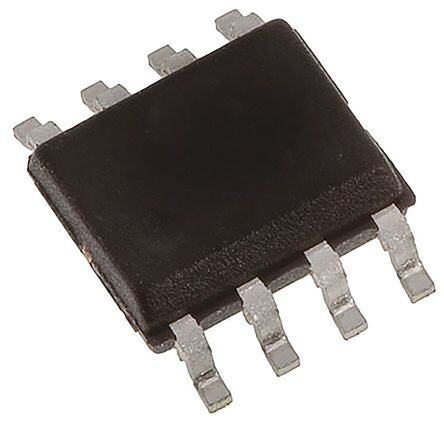
| 描述 | DGTL ISO 4KV 1CH GEN PURP 8SOIC数字隔离器 3.3V/5V High-Speed Digital |
| 产品分类 | |
| IsolatedPower | 无 |
| 品牌 | Texas Instruments |
| 产品手册 | |
| 产品图片 |
|
| rohs | 符合RoHS无铅 / 符合限制有害物质指令(RoHS)规范要求 |
| 产品系列 | 接口 IC,数字隔离器,Texas Instruments ISO721D- |
| 数据手册 | |
| 产品型号 | ISO721D |
| PulseWidthDistortion(Max) | 2ns |
| 上升/下降时间(典型值) | 1ns, 1ns |
| 产品目录页面 | |
| 产品种类 | |
| 传播延迟tpLH/tpHL(最大值) | 24ns, 24ns |
| 传播延迟时间 | 24 ns |
| 供应商器件封装 | 8-SOIC |
| 共模瞬态抗扰度(最小值) | 25kV/µs |
| 其它名称 | 296-19382 |
| 制造商产品页 | http://www.ti.com/general/docs/suppproductinfo.tsp?distId=10&orderablePartNumber=ISO721D |
| 包装 | 管件 |
| 单位重量 | 76 mg |
| 反向通道 | 0 Channel |
| 商标 | Texas Instruments |
| 安装风格 | SMD/SMT |
| 封装 | Tube |
| 封装/外壳 | 8-SOIC(0.154",3.90mm 宽) |
| 封装/箱体 | SOIC-8 |
| 工作温度 | -40°C ~ 125°C |
| 工厂包装数量 | 75 |
| 技术 | 容性耦合 |
| 数据速率 | 100Mbps |
| 最大工作温度 | + 125 C |
| 最大数据速率 | 100 Mb/s |
| 最小工作温度 | - 40 C |
| 标准包装 | 75 |
| 正向通道 | 1 Channel |
| 特色产品 | http://www.digikey.com/cn/zh/ph/Texas-Instruments/iso721d.html |
| 电压-电源 | 3 V ~ 5.5 V |
| 电压-隔离 | 4000Vpk |
| 电源电压-最大 | 5 V |
| 电源电压-最小 | 3.3 V |
| 类型 | 通用 |
| 系列 | ISO721 |
| 绝缘电压 | 4 kVrms |
| 脉宽失真(最大) | 2ns |
| 输入-输入侧1/输入侧2 | 1/0 |
| 通道数 | 1 |
| 通道数量 | 1 Channel |
| 通道类型 | 单向 |
| 配用 | /product-detail/zh/ISO72XEVM/296-20849-ND/1216455 |
| 隔离式电源 | 无 |


- 商务部:美国ITC正式对集成电路等产品启动337调查
- 曝三星4nm工艺存在良率问题 高通将骁龙8 Gen1或转产台积电
- 太阳诱电将投资9.5亿元在常州建新厂生产MLCC 预计2023年完工
- 英特尔发布欧洲新工厂建设计划 深化IDM 2.0 战略
- 台积电先进制程称霸业界 有大客户加持明年业绩稳了
- 达到5530亿美元!SIA预计今年全球半导体销售额将创下新高
- 英特尔拟将自动驾驶子公司Mobileye上市 估值或超500亿美元
- 三星加码芯片和SET,合并消费电子和移动部门,撤换高东真等 CEO
- 三星电子宣布重大人事变动 还合并消费电子和移动部门
- 海关总署:前11个月进口集成电路产品价值2.52万亿元 增长14.8%


PDF Datasheet 数据手册内容提取
Product Sample & Technical Tools & Support & Reference Folder Buy Documents Software Community Design ISO721,ISO721M,ISO722,ISO722M SLLS629L–JANUARY2006–REVISEDOCTOBER2015 ISO72x Single Channel High-Speed Digital Isolators 1 Features If this dc-refresh pulse is not received for more than 4 μs, the input is assumed to be unpowered or not • 100and150-MbpsSignalingRateOptions 1 being actively driven, and the failsafe circuit drives • LowPropagationDelay theoutputtoalogic-highstate. • LowPulseSkew The symmetry of the dielectric and capacitor within • Low-PowerSleepMode the integrated circuitry provides for close capacitive • HighElectromagneticImmunity matching, and allows fast transient voltage changes between the input and output grounds without • LowInput-CurrentRequirement corrupting the output. The small capacitance and • FailsafeOutput resulting time constant provide for fast operation with • Drop-InReplacementforMostOptoandMagnetic signaling rates from 0 Mbps (DC) to 100 Mbps for the Isolators ISO721 and the ISO722 devices, and 0 Mbps to 150 MbpswiththeISO721MandtheISO722Mdevices. • Operatesfrom3.3Vand5VSupplies • -40°Cto125°COperatingTemperatureRange These devices require two supply voltages of 3.3 V, 5 V, or any combination. All inputs are 5-V tolerant • 50kV/µsTransientImmunity,Typical when supplied from a 3.3-V supply and all outputs • SafetyandRegulatoryApprovals are4mACMOS. – VDEBasicInsulationwith4000-V V ,560 PK IOTM The ISO722 and ISO722M devices include an active- V V PK IORM low output enable that when driven to a high logic – 2500V IsolationperUL1577 level, places the output in a high-impedance state RMS – CSAApprovedforComponentAcceptance andturnsoffinternalbiascircuitrytoconservepower. Notice5AandIEC60950-1 Both the ISO721 and ISO722 devices have TTL input thresholds and a noise filter at the input that prevent 2 Applications transient pulses of up to 2 ns in duration from being passedtotheoutputofthedevice. • IndustrialFieldbus – Modbus The ISO721M and ISO722M devices have CMOS V / 2 input thresholds, but do not have the noise- – Profibus CC filter and the additional propagation delay. These – DeviceNet™DataBuses features of the ISO721M device also provide for – SmartDistributedSystems(SDS™) reduced-jitteroperation. • ComputerPeripheralInterface The ISO721, ISO721M, ISO722, and ISO722M • ServoControlInterface devices are characterized for operation over the ambienttemperaturerangeof–40°Cto125°C. • DataAcquisition DeviceInformation(1) 3 Description PARTNUMBER PACKAGE BODYSIZE(NOM) The ISO721, ISO721M, ISO722, and ISO722M are ISO721 SOP(8) 9.50mmx6.57mm digital isolators with a logic input and output buffer separated by a silicon dioxide (SiO ) insulation ISO721 2 barrier. This barrier provides galvanic isolation of up ISO721M SOIC(8) 4.90mmx3.91mm to 4000 VPK per VDE. Used in conjunction with ISO722 isolated power supplies, these devices prevent noise ISO722M currents on a data bus or other circuits from entering the local ground, and interfering with or damaging (1) For all available packages, see the orderable addendum at theendofthedatasheet. sensitivecircuitry. A binary input signal is conditioned, translated to a SimplifiedSchematic balanced signal, then differentiated by the capacitive isolation barrier. Across the isolation barrier, a VCC1 Isolation VCC2 differential comparator receives the logic transition Capacitor information, then sets or resets a flip-flop and the IN OUT output circuit accordingly. A periodic update pulse is sent across the barrier to ensure the proper dc level EN (ISO722/M-only) oftheoutput. GND1 GND2 1 An IMPORTANT NOTICE at the end of this data sheet addresses availability, warranty, changes, use in safety-critical applications, intellectualpropertymattersandotherimportantdisclaimers.PRODUCTIONDATA.
ISO721,ISO721M,ISO722,ISO722M SLLS629L–JANUARY2006–REVISEDOCTOBER2015 www.ti.com Table of Contents 1 Features.................................................................. 1 8 ParameterMeasurementInformation................15 2 Applications........................................................... 1 9 DetailedDescription............................................ 18 3 Description............................................................. 1 9.1 Overview.................................................................18 4 RevisionHistory..................................................... 2 9.2 FunctionalBlockDiagram.......................................18 5 DeviceComparisonTable..................................... 4 9.3 FeaturesDescription...............................................19 9.4 DeviceFunctionalModes........................................21 6 PinConfigurationandFunctions......................... 4 10 ApplicationandImplementation........................ 22 7 Specifications......................................................... 5 10.1 ApplicationInformation..........................................22 7.1 AbsoluteMaximumRatings .....................................5 10.2 TypicalApplication................................................22 7.2 ESDRatings ............................................................5 11 PowerSupplyRecommendations..................... 24 7.3 RecommendedOperatingConditions.......................5 7.4 ThermalInformation..................................................6 12 Layout................................................................... 24 7.5 ElectricalCharacteristics,5V...................................6 12.1 LayoutGuidelines.................................................24 7.6 ElectricalCharacteristics,5V,3.3V.........................7 12.2 LayoutExample....................................................25 7.7 ElectricalCharacteristics,3.3V,5V.........................7 13 DeviceandDocumentationSupport................. 26 7.8 ElectricalCharacteristics,3.3V ...............................8 13.1 DocumentationSupport .......................................26 7.9 PowerDissipation.....................................................8 13.2 RelatedLinks........................................................26 7.10 SwitchingCharacteristics,5V................................9 13.3 Trademarks...........................................................26 7.11 SwitchingCharacteristics,5V,3.3V....................10 13.4 ElectrostaticDischargeCaution............................26 7.12 SwitchingCharacteristics,3.3V,5V....................11 13.5 Glossary................................................................26 7.13 SwitchingCharacteristics,3.3V ..........................12 14 Mechanical,Packaging,andOrderable 7.14 TypicalCharacteristics..........................................13 Information........................................................... 26 4 Revision History NOTE:Pagenumbersforpreviousrevisionsmaydifferfrompagenumbersinthecurrentversion. ChangesfromRevisionK(February2012)toRevisionL Page • MovedPowerDissipationmetricintonewtable,calledPowerDissipation .......................................................................... 8 • Addedheaderrowabove"V "rowwiththetext"DINVVDEV0884-10(VDEV0884-10):2006-12"inthe IORM InsulationCharacteristicstable............................................................................................................................................. 19 • Added"UL1577"headerrowover"V "rowintheInsulationCharacteristicstable......................................................... 19 ISO • Moved"V "rowtothebottomoftheInsulationCharacteristicstable. ............................................................................. 19 ISO • Deleted"perUL"in"Isolationvoltage"intheInsulationCharacteristicstable. ................................................................... 19 • ChangedtheD-8MINvalueofL(101)from"4.8"to"4"inthePackageInsulationCharacteristicstable. ......................... 20 • ChangedtheD-8MINvalueofL(102)from"4.3"to"4"inthePackageInsulationCharacteristicstable. ......................... 20 • ChangedTestCondition"DINIEC60112/VDE0303Part1"to"DINEN60112(VDE0303-11);IEC60112"inthe PackageInsulationCharacteristicstable............................................................................................................................. 20 • DeletedbottomrowofthePackageInsulationCharacteristicstable. ................................................................................. 20 ChangesfromRevisionJ(July2010)toRevisionK Page • AddedESDRatingtable,FeatureDescriptionsection,DeviceFunctionalModes,ApplicationandImplementation section,PowerSupplyRecommendationssection,Layoutsection,DeviceandDocumentationSupportsection,and Mechanical,Packaging,andOrderableInformation............................................................................................................... 1 • ChangedtheTitleFrom:3.3-V/5-VHigh-SpeedDigitalIsolatorsTo:ISO72xSingleChannelHigh-SpeedDigital Isolators.................................................................................................................................................................................. 1 • ChangedtheFeaturesList .................................................................................................................................................... 1 • ChangedthesecondparagraphoftheDescriptionFrom:"4000V"To:"4000V perVDE..."............................................ 1 PK • ChangedtheThermalInformationtable................................................................................................................................. 6 • ChangedFigure1................................................................................................................................................................. 13 • ChangedtheBasicisolationgroupSpecificationFrom:IIIaTo:IIinIEC60664-1RatingsTable....................................... 19 2 SubmitDocumentationFeedback Copyright©2006–2015,TexasInstrumentsIncorporated ProductFolderLinks:ISO721 ISO721M ISO722 ISO722M
ISO721,ISO721M,ISO722,ISO722M www.ti.com SLLS629L–JANUARY2006–REVISEDOCTOBER2015 • ChangedVDEtextFrom:"DINEN60747-5-5(VDE0884-5)"To:"DINVVDEV0884-10(VDEV0884-10):2006-12" intheRegulatoryInformationtable....................................................................................................................................... 19 • ChangedCSAFilenumber:1698195To:220991intheRegulatoryInformationtable....................................................... 19 • ChangedtheC MINvalueFrom:≥175VTo:400VinthePackageInsulationCharacteristicstable.............................. 20 TI • ChangedR TestConditionFrom:T <100°CTo:T =25°CinPackageInsulationCharacteristics .............................. 20 IO A A • MovedtheR valuesfromtheTYPcolumntotheMINcolumnofPackageInsulationCharacteristics ............................ 20 IO • ChangedthetitleofFigure16From:θ ThermalDeratingCurveperDINEN60747-5-5To:θ ThermalDerating JC JC CurveperVDE..................................................................................................................................................................... 20 • ChangedTable1,addedrowX,PD,X,Undetermined....................................................................................................... 21 • ChangedTable2,addedrowX,PD,X,Undetermined....................................................................................................... 21 • ChangedFigure17 .............................................................................................................................................................. 21 ChangesfromRevisionI(February2010)toRevisionJ Page • ChangedNote1oftheElectricalCharacteristics,5Vtable.................................................................................................. 6 • ChangedNote1oftheElectricalCharacteristics,5V,3.3Vtable........................................................................................ 7 • ChangedNote1oftheElectricalCharacteristics,3.3V,5Vtable........................................................................................ 7 • ChangedNote1oftheElectricalCharacteristics,3.3Vtable............................................................................................... 8 • ChangedVtoVpeakinUNITcolumnofIECInsulationCharacteristicstable..................................................................... 19 • AddedrowforV toInsulationCharacteristicstable......................................................................................................... 19 ISO • ChangedthetitleFrom:PackageCharacteristicsTo:PackageInsulationCharacteristics................................................. 20 ChangesfromRevisionH(June2009)toRevisionI Page • ChangedFeaturesFrom:50kV/sTransientImmunity,TypicalTo:50kV/µsTransientImmunity,Typical.......................... 1 ChangesfromRevisionG(December2008)toRevisionH Page • ChangedthefirstparagraphoftheDescriptionFrom:"siliconoxide(SiO ).."To:"silicondioxide(SiO ).."..........................1 2 2 • AddedtheDUB8pinpackagetothePinConfigurationandFunctions................................................................................ 4 • AddedpackagedesignatorsD-8andDUB-8tothetableDescriptions/TestConditionsofthePackageInsulation Characteristicstable............................................................................................................................................................. 20 ChangesfromRevisionF(November2008)toRevisionG Page • ChangedtheFeaturesListFrom:4000-V IsolationTo:4000-V Isolation,560-V V ...................................... 1 (peak) (peak) peak IORM ChangesfromRevisionE(May2008)toRevisionF Page • ChangedFigure19textFrom:20mmmax.fromV To:2mmmax.fromV .............................................................. 23 CC1 CC1 • ChangedNoteinTable3From:TheISO72xpin1andpin3areinternallyconnectedtogether.Eitherorbothmay beusedasV .To:Pin1shouldbeusedasV .Pin3mayalsobeusedasV orleftopenaslongasPin1is CC1 CC1 CC1 connectedtoV ................................................................................................................................................................ 23 CC1 • ChangedNoteinTable3From:TheISO721andISO721Mpin5andpin7areinternallyconnectedtogether.Either orbothmaybeusedasGND2.To:Pin5shouldbeusedasGND2.Pin7mayalsobeusedasGND2orleftopen aslongasPin5isconnectedtoGND2............................................................................................................................... 23 Copyright©2006–2015,TexasInstrumentsIncorporated SubmitDocumentationFeedback 3 ProductFolderLinks:ISO721 ISO721M ISO722 ISO722M
ISO721,ISO721M,ISO722,ISO722M SLLS629L–JANUARY2006–REVISEDOCTOBER2015 www.ti.com ChangesfromRevisionD(February2007)toRevisionE Page • ChangedchangedtheV MINvalueFrom:4.5VTo:3VintheRecommendedOperatingConditionstable ...................5 CC • AddedNote1totheRecommendedOperatingConditionstable.......................................................................................... 5 • AddedNote1totheElectricalCharacteristics,5Vtable....................................................................................................... 6 • AddedNote1totheElectricalCharacteristics,5V,3.3Vtable ........................................................................................... 7 • AddedNote1totheElectricalCharacteristics,3.3V,5Vtable............................................................................................ 7 • AddedNote1totheElectricalCharacteristics,3.3Vtable.................................................................................................... 8 4 SubmitDocumentationFeedback Copyright©2006–2015,TexasInstrumentsIncorporated ProductFolderLinks:ISO721 ISO721M ISO722 ISO722M
ISO721,ISO721M,ISO722,ISO722M www.ti.com SLLS629L–JANUARY2006–REVISEDOCTOBER2015 5 Device Comparison Table OUTPUT INPUT NOISE PRODUCT SIGNALINGRATE ENABLED THRESHOLDS FILTER ISO721 100Mbps NO TTL YES ISO721M 150Mbps NO CMOS NO ISO722 100Mbps YES TTL YES ISO722M 150Mbps YES CMOS NO 6 Pin Configuration and Functions ISO721,ISO721M SOIC(D)Package ISO722,ISO722M TopView SOIC(D)Package TopView VCC1 1 8 VCC2 VCC1 1 8 VCC2 V IN 23 olation 76 GONUDT2 IN 2 ation 7 EN CC1 Is VCC1 3 sol 6 OUT GND1 4 5 GND2 I GND1 4 5 GND2 ISO721 SOP(DUB)Package TopView VCC1 1 8 VCC2 IN 2 on 7 GND2 ati VCC1 3 sol 6 OUT I GND1 4 5 GND2 PinFunctions PIN ISO721x ISO722x I/O DESCRIPTION NAME NO. NO. V 1,3 1,3 - Powersupply,V CC1 CC1 V 8 8 - Powersupply,V CC2 CC2 IN 2 2 I Input OUT 6 6 O Output Outputenable.OUTisenabledwhenENislowordisconnectedanddisabled EN - 7 I whenENishigh. GND1 4 4 - GroundconnectionforV CC1 GND2 5,7 5 - GroundconnectionforV CC2 Copyright©2006–2015,TexasInstrumentsIncorporated SubmitDocumentationFeedback 5 ProductFolderLinks:ISO721 ISO721M ISO722 ISO722M
ISO721,ISO721M,ISO722,ISO722M SLLS629L–JANUARY2006–REVISEDOCTOBER2015 www.ti.com 7 Specifications 7.1 Absolute Maximum Ratings overoperatingfree-airtemperaturerange(unlessotherwisenoted)(1) MIN MAX UNIT V Supplyvoltage V ,V –0.5 6 V CC CC1 CC2 V Inputvoltage IN,OUT,orEN –0.5 V +0.5(2) V I CC I Outputcurrent ±15 mA O T Maximumjunctiontemperature 170 °C J T Storagetemperature –65 150 °C stg (1) StressesbeyondthoselistedunderAbsoluteMaximumRatingsmaycausepermanentdamagetothedevice.Thesearestressratings only,andfunctionaloperationofthedeviceattheseoranyotherconditionsbeyondthoseindicatedunderRecommendedOperating Conditionsisnotimplied.Exposuretoabsolute-maximum-ratedconditionsforextendedperiodsmayaffectdevicereliability. (2) Maximumvoltagemustnotexceed6V. 7.2 ESD Ratings VALUE UNIT Humanbodymodel(HBM),perANSI/ESDA/JEDECJS-001(1) ±2000 V(ESD) Electrostaticdischarge Chargeddevicemodel(CDM),perJEDECspecificationJESD22- V C101(2) ±1000 (1) JEDECdocumentJEP155statesthat500-VHBMallowssafemanufacturingwithastandardESDcontrolprocess. (2) JEDECdocumentJEP157statesthat250-VCDMallowssafemanufacturingwithastandardESDcontrolprocess. 7.3 Recommended Operating Conditions MIN TYP MAX UNIT V Supplyvoltage(1),V ,V 3 5.5 V CC CC1 CC2 I 4 mA OH Outputcurrent I –4 mA OL ISO72x 10 t Inputpulseduration ns ui ISO72xM 6.67 ISO72x 0 100 1/t SignalingRate Mbps ui ISO72xM 0 150 V High-levelinputvoltage(IN,EN) 2 5.5 V IH ISO72x V Low-levelinputvoltage(IN,EN) 0 0.8 V IL V High-levelinputvoltage(IN,EN) 0.7V V V IH CC CC IOS72xM V Low-levelinputvoltage(IN,EN) 0 0.3V V IL CC T Ambienttemperature –40 25 125 °C A T Junctiontemperature SeeThermalInformation 150 °C J ExternalmagneticfieldintensityperIEC61000-4-8andIEC61000-4-9 H 1000 A/m certification (1) Forthe5-Voperation,V orV isspecifiedfrom4.5Vto5.5V.Forthe3-Voperation,V orV isspecifiedfrom3Vto3.6V. CC1 CC2 CC1 CC2 6 SubmitDocumentationFeedback Copyright©2006–2015,TexasInstrumentsIncorporated ProductFolderLinks:ISO721 ISO721M ISO722 ISO722M
ISO721,ISO721M,ISO722,ISO722M www.ti.com SLLS629L–JANUARY2006–REVISEDOCTOBER2015 7.4 Thermal Information ISO721 ISO72x THERMALMETRIC(1) DUB D UNIT 8PINS 8PINS R High-KBoard 86.6 114.7 θJA Junction-to-ambientthermalresistance °C/W Low-KBoard N/A 263 R Junction-to-case(top)thermalresistance 70.3 63 °C/W θJC(top) R Junction-to-boardthermalresistance 50.2 54.8 °C/W θJB ψ Junction-to-topcharacterizationparameter 34.3 18.9 °C/W JT ψ Junction-to-boardcharacterizationparameter 49.8 54.3 °C/W JB R Junction-to-case(bottom)thermalresistance N/A N/A °C/W θJC(bot) (1) Formoreinformationabouttraditionalandnewthermalmetrics,seetheICPackageThermalMetricsapplicationreport,SPRA953. 7.5 Electrical Characteristics, 5 V V andV at5V±10%(overrecommendedoperatingconditionsunlessotherwisenoted.) CC1 CC2 PARAMETER TESTCONDITIONS MIN TYP MAX UNIT Quiescent 0.5 1 I V supplycurrent V =V or0V,noload mA CC1 CC1 I CC 25Mbps 2 4 ISO722/722MSleepMode ENatV 200 μA CC V =V or0V, I CC I V supplycurrent Quiescent Noload ENat0Vor 8 12 CC2 CC2 ISO721/721M mA 25Mbps V =V or0V,noload 10 14 I CC I =–4mA,SeeFigure10 V –0.8 4.6 OH CC V High-leveloutputvoltage V OH I =–20μA,SeeFigure10 V –0.1 5 OH CC I =4mA,SeeFigure10 0.2 0.4 OL V Low-leveloutputvoltage V OL I =20μA,SeeFigure10 0 0.1 OL V Inputvoltagehysteresis 150 mV I(HYS) I High-levelinputcurrent EN,INat2V 10 IH μA I Low-levelinputcurrent EN,INat0.8V –10 IL High-impedance I ISO722,ISO722M EN,INatV 1 μA OZ outputcurrent CC C Inputcapacitancetoground INatV ,V =0.4sin(4×10⁶πt) 1 pF I CC I CMTI Common-modetransientimmunity V =V or0V,SeeFigure14 25 50 kV/μs I CC Copyright©2006–2015,TexasInstrumentsIncorporated SubmitDocumentationFeedback 7 ProductFolderLinks:ISO721 ISO721M ISO722 ISO722M
ISO721,ISO721M,ISO722,ISO722M SLLS629L–JANUARY2006–REVISEDOCTOBER2015 www.ti.com 7.6 Electrical Characteristics, 5 V, 3.3 V V at5V±10%,V at3.3V±10%(overrecommendedoperatingconditionsunlessotherwisenoted.) CC1 CC2 PARAMETER TESTCONDITIONS MIN TYP MAX UNIT Quiescent 0.5 1 I V supplycurrent V =V or0V,noload mA CC1 CC1 I CC 25Mbps 2 4 ISO722/722M ENatV 150 μA Sleepmode V =V or0V, CC I CC I V supplycurrent Noload ENat0Vor CC2 CC2 Quiescent 4 6.5 ISO721/721M mA 25Mbps V =V or0V,noload 5 7.5 I CC I =–4mA,SeeFigure10 V –0.4 3 OH CC V High-leveloutputvoltage V OH I =–20μA,SeeFigure10 V –0.1 3.3 OH CC I =4mA,SeeFigure10 0.2 0.4 OL V Low-leveloutputvoltage V OL I =20μA,SeeFigure10 0 0.1 OL V Inputvoltagehysteresis 150 mV I(HYS) I High-levelinputcurrent EN,INat2V 10 μA IH I Low-levelinputcurrent EN,INat0.8V –10 μA IL High-impedance I ISO722,ISO722M EN,INatV 1 μA OZ outputcurrent CC C Inputcapacitancetoground INatV ,V =0.4sin(4×10⁶πt) 1 pF I CC I CMTI Common-modetransientimmunity V =V or0V,SeeFigure14 25 40 kV/μs I CC 7.7 Electrical Characteristics, 3.3 V, 5 V V at3.3V±10%,V at5V±10%(overrecommendedoperatingconditionsunlessotherwisenoted.) CC1 CC2 PARAMETER TESTCONDITIONS MIN TYP MAX UNIT Quiescent 0.3 0.5 I V supplycurrent V =V or0V,noload mA CC1 CC1 I CC 25Mbps 1 2 ISO722/722M ENatV 200 μA Sleepmode CC V =V or0V, I CC I V supplycurrent Noload ENat0Vor CC2 CC2 Quiescent ISO721/721 8 12 M mA 25Mbps V =V or0V,Noload 10 14 I CC I =–4mA,SeeFigure10 V –0.8 4.6 OH CC V High-leveloutputvoltage V OH I =–20μA,SeeFigure10 V –0.1 5 OH CC I =4mA,SeeFigure10 0.2 0.4 OL V Low-leveloutputvoltage V OL I =20μA,SeeFigure10 0 0.1 OL V Inputvoltagehysteresis 150 mV I(HYS) I High-levelinputcurrent EN,INat2V 10 μA IH I Low-levelinputcurrent EN,INat0.8V –10 μA IL High-impedance I ISO722,ISO722M EN,INatV 1 μA OZ outputcurrent CC C Inputcapacitancetoground INatV ,V =0.4sin(4×10⁶πt) 1 pF I CC I CMTI Common-modetransientimmunity V =V or0V,SeeFigure14 25 40 kV/μs I CC 8 SubmitDocumentationFeedback Copyright©2006–2015,TexasInstrumentsIncorporated ProductFolderLinks:ISO721 ISO721M ISO722 ISO722M
ISO721,ISO721M,ISO722,ISO722M www.ti.com SLLS629L–JANUARY2006–REVISEDOCTOBER2015 7.8 Electrical Characteristics, 3.3 V V andV at3.3V±10%(overrecommendedoperatingconditionsunlessotherwisenoted.) CC1 CC2 PARAMETER TESTCONDITIONS MIN TYP MAX UNIT Quiescent 0.3 0.5 I V supplycurrent V =V or0V,noload mA CC1 CC1 I CC 25Mbps 1 2 ISO722/722M ENatV 150 μA SleepMode CC VI=VCCor0V, ENat0V I V supplycurrent Noload or CC2 CC2 Quiescent 4 6.5 ISO721/721 mA M 25Mbps V =V or0V,noload 5 7.5 I CC I =–4mA,SeeFigure10 V –0.4 3 OH CC V High-leveloutputvoltage V OH I =–20μA,SeeFigure10 V –0.1 3.3 OH CC I =4mA,SeeFigure10 0.2 0.4 OL V Low-leveloutputvoltage V OL I =20μA,SeeFigure10 0 0.1 OL V Inputvoltagehysteresis 150 mV I(HYS) I High-levelinputcurrent EN,INat2V 10 μA IH I Low-levelinputcurrent EN,INat0.8V –10 μA IL High-impedance I ISO722,ISO722M EN,INatV 1 μA OZ outputcurrent CC C Inputcapacitancetoground INatV ,V =0.4sin(4×10⁶πt) 1 pF I CC I CMTI Common-modetransientimmunity V =V or0V,SeeFigure14 25 40 kV/μs I CC 7.9 Power Dissipation overoperatingfree-airtemperaturerange(unlessotherwisenoted) PARAMETER TESTCONDITIONS ISO721 ISO72x UNIT DUB D 8PINS 8PINS VCC1=VCC2=5.5V,TJ= 150°C,CL=15pF,Inputa ISO72x 159 mW 100-Mbps50%duty-cycle squarewave VCC1=VCC2=5.5V,TJ= 150°C,CL=15pF,Inputa P PowerDissipation ISO72xM 195 mW D 100-Mbps50%duty-cycle squarewave VCC1=VCC2=5.5V,TJ= 150°C,CL=15pF,Inputa ISO721 159 mW 100-Mbps50%duty-cycle squarewave Copyright©2006–2015,TexasInstrumentsIncorporated SubmitDocumentationFeedback 9 ProductFolderLinks:ISO721 ISO721M ISO722 ISO722M
ISO721,ISO721M,ISO722,ISO722M SLLS629L–JANUARY2006–REVISEDOCTOBER2015 www.ti.com 7.10 Switching Characteristics, 5 V V andV at5V±10%(overrecommendedoperatingconditionsunlessotherwisenoted.) CC1 CC2 PARAMETER TESTCONDITIONS MIN TYP MAX UNIT t Propagationdelay,low-to-high-leveloutput 13 17 24 ns PLH t Propagationdelay,high-to-low-leveloutput ISO72x 13 17 24 ns PHL tsk(p) Pulseskew|tPHL–tPLH| ENat0V, 0.5 2 ns t Propagationdelay,low-to-high-leveloutput SeeFigure10 8 10 16 ns PLH t Propagationdelay,high-to-low-leveloutput ISO72xM 8 10 16 ns PHL t Pulseskew|t –t | 0.5 1 ns sk(p) PHL PLH t (1) Part-to-partskew 0 3 ns sk(pp) tr Outputsignalrisetime ENat0V, 1 ns t Outputsignalfalltime SeeFigure10 1 f Sleep-modepropagationdelay, t 6 8 15 ns pHZ high-level-to-high-mpedanceoutput SeeFigure11 Sleep-modepropagationdelay, t 3.5 4 8 μs pZH high-impedance-to-high-leveloutput ISO722 Sleep-modepropagationdelay, ISO722M t 5.5 8 15 ns pLZ low-level-to-high-impedanceoutput SeeFigure12 Sleep-modepropagationdelay, t 4 5 8 μs pZL high-impedance-to-low-leveloutput t Failsafeoutputdelaytimefrominputpowerloss SeeFigure13 3 μs fs 100-MbpsNRZdatainput,SeeFigure15 2 ISO72x 100-Mbpsunrestrictedbitrunlengthdata 3 input,SeeFigure15 t Peak-to-peakeye-patternjitter ns jit(PP) 150-MbpsNRZdatainput,SeeFigure15 1 ISO72xM 150-Mbpsunrestrictedbitrunlengthdata 2 input,SeeFigure15 (1) t isthemagnitudeofthedifferenceinpropagationdelaytimesbetweenanyspecifiedterminalsoftwodeviceswhenbothdevices sk(PP) operatewiththesamesupplyvoltages,atthesametemperature,andhaveidenticalpackagesandtestcircuits. 10 SubmitDocumentationFeedback Copyright©2006–2015,TexasInstrumentsIncorporated ProductFolderLinks:ISO721 ISO721M ISO722 ISO722M
ISO721,ISO721M,ISO722,ISO722M www.ti.com SLLS629L–JANUARY2006–REVISEDOCTOBER2015 7.11 Switching Characteristics, 5 V, 3.3 V V at5V±10%,V at3.3V±10%(overrecommendedoperatingconditionsunlessotherwisenoted.) CC1 CC2 PARAMETER TESTCONDITIONS MIN TYP MAX UNIT t Propagationdelay,low-to-high-leveloutput 15 19 30 ns PLH t Propagationdelay,high-to-low-leveloutput ISO72x 15 19 30 ns PHL tsk(p) Pulseskew|tPHL–tPLH| ENat0V, 0.5 3 ns t Propagationdelay,low-to-high-leveloutput SeeFigure10 10 12 20 ns PLH t Propagationdelay,high-to-low-leveloutput ISO72xM 10 12 20 ns PHL t Pulseskew|t –t | 0.5 1 ns sk(p) PHL PLH t (1) Part-to-partskew 0 5 ns sk(pp) tr Outputsignalrisetime ENat0V, 2 ns t Outputsignalfalltime SeeFigure10 2 ns f Sleep-modepropagationdelay, t 7 11 25 ns pHZ high-level-to-high-mpedanceoutput SeeFigure11 Sleep-modepropagationdelay, t 4.5 6 8 μs pZH high-impedance-to-high-leveloutput ISO722 Sleep-modepropagationdelay, ISO722M t 7 13 25 ns pLZ low-level-to-high-impedanceoutput SeeFigure12 Sleep-modepropagationdelay, t 4.5 6 8 μs pZL high-impedance-to-low-leveloutput t Failsafeoutputdelaytimefrominputpowerloss SeeFigure13 3 μs fs 100-MbpsNRZdatainput,SeeFigure15 2 ISO72x 100-Mbpsunrestrictedbitrunlengthdata 3 input,SeeFigure15 t Peak-to-peakeye-patternjitter ns jit(PP) 150-MbpsNRZdatainput,SeeFigure15 1 ISO72xM 150-Mbpsunrestrictedbitrunlengthdata 2 input,SeeFigure15 (1) t isthemagnitudeofthedifferenceinpropagationdelaytimesbetweenanyspecifiedterminalsoftwodeviceswhenbothdevices sk(PP) operatewiththesamesupplyvoltages,atthesametemperature,andhaveidenticalpackagesandtestcircuits. Copyright©2006–2015,TexasInstrumentsIncorporated SubmitDocumentationFeedback 11 ProductFolderLinks:ISO721 ISO721M ISO722 ISO722M
ISO721,ISO721M,ISO722,ISO722M SLLS629L–JANUARY2006–REVISEDOCTOBER2015 www.ti.com 7.12 Switching Characteristics, 3.3 V, 5 V V at3.3V±10%,V at5V±10%(overrecommendedoperatingconditionsunlessotherwisenoted.) CC1 CC2 PARAMETER TESTCONDITIONS MIN TYP MAX UNIT t Propagationdelay,low-to-high-leveloutput 15 17 30 ns PLH t Propagationdelay,high-to-low-leveloutput ISO72x 15 17 30 ns PHL tsk(p) Pulseskew|tPHL–tPLH| ENat0V, 0.5 2 ns t Propagationdelay,low-to-high-leveloutput SeeFigure10 10 12 21 ns PLH t Propagationdelay,high-to-low-leveloutput ISO72xM 10 12 21 ns PHL t Pulseskew|t –t | 0.5 1 ns sk(p) PHL PLH t (1) Part-to-partskew 0 5 ns sk(pp) tr Outputsignalrisetime ENat0V, 1 ns t Outputsignalfalltime SeeFigure10 1 ns f Sleep-modepropagationdelay, t 7 9 15 ns pHZ high-level-to-high-mpedanceoutput SeeFigure11 Sleep-modepropagationdelay, t 4.5 5 8 μs pZH high-impedance-to-high-leveloutput ISO722 Sleep-modepropagationdelay, ISO722M t 7 9 15 ns pLZ low-level-to-high-impedanceoutput SeeFigure12 Sleep-modepropagationdelay, t 4.5 5 8 μs pZL high-impedance-to-low-leveloutput t Failsafeoutputdelaytimefrominputpowerloss SeeFigure13 3 μs fs 100-MbpsNRZdatainput,SeeFigure15 2 ISO72x 100-Mbpsunrestrictedbitrunlengthdata 3 input,SeeFigure15 t Peak-to-peakeye-patternjitter ns jit(PP) 150-MbpsNRZdatainput,SeeFigure15 1 ISO72xM 150-Mbpsunrestrictedbitrunlengthdata 2 input,SeeFigure15 (1) t isthemagnitudeofthedifferenceinpropagationdelaytimesbetweenanyspecifiedterminalsoftwodeviceswhenbothdevices sk(PP) operatewiththesamesupplyvoltages,atthesametemperature,andhaveidenticalpackagesandtestcircuits. 12 SubmitDocumentationFeedback Copyright©2006–2015,TexasInstrumentsIncorporated ProductFolderLinks:ISO721 ISO721M ISO722 ISO722M
ISO721,ISO721M,ISO722,ISO722M www.ti.com SLLS629L–JANUARY2006–REVISEDOCTOBER2015 7.13 Switching Characteristics, 3.3 V V andV at3.3V±10%(overrecommendedoperatingconditionsunlessotherwisenoted.) CC1 CC2 PARAMETER TESTCONDITIONS MIN TYP MAX UNIT t Propagationdelay,low-to-high-leveloutput 17 20 34 ns PLH t Propagationdelay,high-to-low-leveloutput ISO72x 17 20 34 ns PHL tsk(p) Pulseskew|tPHL–tPLH| ENat0V, 0.5 3 ns t Propagationdelay,low-to-high-leveloutput SeeFigure10 10 12 25 ns PLH t Propagationdelay,high-to-low-leveloutput ISO72xM 10 12 25 ns PHL t Pulseskew|t –t | 0.5 1 ns sk(p) PHL PLH t (1) Part-to-partskew 0 5 ns sk(pp) tr Outputsignalrisetime ENat0V, 2 ns t Outputsignalfalltime SeeFigure10 2 f Sleep-modepropagationdelay, t 7 13 25 ns pHZ high-level-to-high-mpedanceoutput SeeFigure11 Sleep-modepropagationdelay, t 5 6 8 µs pZH high-impedance-to-high-leveloutput ISO722 Sleep-modepropagationdelay, ISO722M t 7 13 25 ns pLZ low-level-to-high-impedanceoutput SeeFigure12 Sleep-modepropagationdelay, t 5 6 8 μs pZL high-impedance-to-low-leveloutput t Failsafeoutputdelaytimefrominputpowerloss SeeFigure13 3 μs fs 100-MbpsNRZdatainput,SeeFigure15 2 ISO72x 100-Mbpsunrestrictedbitrunlengthdata 3 input,SeeFigure15 t Peak-to-peakeye-patternjitter ns jit(PP) 150-MbpsNRZdatainput,SeeFigure15 1 ISO72xM 150-Mbpsunrestrictedbitrunlengthdata 2 input,SeeFigure15 (1) t isthemagnitudeofthedifferenceinpropagationdelaytimesbetweenanyspecifiedterminalsoftwodeviceswhenbothdevices sk(PP) operatewiththesamesupplyvoltages,atthesametemperature,andhaveidenticalpackagesandtestcircuits. Copyright©2006–2015,TexasInstrumentsIncorporated SubmitDocumentationFeedback 13 ProductFolderLinks:ISO721 ISO721M ISO722 ISO722M
ISO721,ISO721M,ISO722,ISO722M SLLS629L–JANUARY2006–REVISEDOCTOBER2015 www.ti.com 7.14 Typical Characteristics 9 15 VCC1= 3.3 V, 14 VCC1= 5 V, 8 VCC2= 3.3 V, 13 VCC2= 5 V, A)RMS 7 TCAL== 2155o Cp,F A)RMS 1121 TCAL== 2155o Cp,F ICC2 pply Current−(m 456 ICC2 pply Current−(m 167890 ICC1 Su− 3 ICC1 Su− 45 ICC 2 ICC 3 2 1 1 0 0 0 20 40 60 80 100 0 25 50 75 100 Signaling Rate (Mbps) Signaling Rate (Mbps) Figure1.RMSSupplyCurrentvsSignalingRate Figure2.RMSSupplyCurrentvsSignalingRate 30 20 tPLH 18 tPLH 25 16 ISO72x tPHL ISO72x tPHL ns 20 ns 14 − − elay tPLH elay 12 tPLH on D 15 tPHL on D 10 ISO72xM tPHL ati ISO72xM ati 8 g g Propa 10 VCC1= 3.3 V, Propa 6 VCC1= 5 V, 5 VCCLC=2 1=5 3 p.3F ,V, 4 VCCLC=2 1=5 5 p VF,, Air Flow at 7 cf/m 2 Air Flow at 7 cf/m 0 0 -40 -25 -10 5 20 35 50 65 80 95 110 125 -40 -25 -10 5 20 35 50 65 80 95 110 125 TA−Free-Air Temperature−oC TA−Free-Air Temperature−oC Figure3.PropagationDelayvsFree-AirTemperature Figure4.PropagationDelayvsFree-AirTemperature 1.4 2.5 1.35 5-V (VIT+) 2.4 5-V (VIT+) V V 2.3 − − d 1.3 d hol 3.3-V (VIT+) hol 2.2 5-V (VIT-) s s hre 1.25 hre 2.1 T T e e 2 ag 1.2 ag Air Flow at 7 cf/m olt Air Flow at 7 cf/m olt 1.9 V V ut 1.15 ut 1.8 p p −In 1.1 5-V (VIT-) −In 1.7 3.3-V (VIT+) VIT VIT 1.6 1.05 3.3-V (VIT-) 1.5 3.3-V (VIT-) 1 1.4 -40 -25 -10 5 20 35 50 65 80 95 110 125 -40 -25 -10 5 20 35 50 65 80 95 110 125 TA−Free-Air Temperature−oC TA−Free-Air Temperature−oC Figure5.ISO72xInputThresholdVoltagevsFree-Air Figure6.ISO72xMInputThresholdVoltagevsFree-Air Temperature Temperature 14 SubmitDocumentationFeedback Copyright©2006–2015,TexasInstrumentsIncorporated ProductFolderLinks:ISO721 ISO721M ISO722 ISO722M
ISO721,ISO721M,ISO722,ISO722M www.ti.com SLLS629L–JANUARY2006–REVISEDOCTOBER2015 Typical Characteristics (continued) 2.92 -80 2.9 mA -70 VCC= 5 V TA= 25oC − e−V 2.88 Vfs+ urrent -60 g C -50 FailsafeVolta 22..8864 VCACiLrC F==l o1 55w V pa Fto, 7r 3c.f3/m V, Level Output --3400 VCC= 3.3 V VCC1 2.82 High- -20 Vfs- −H 2.8 IO -10 2.78 0 -40 -25 -10 5 20 35 50 65 80 95 110 125 0 1 2 3 4 5 6 TA−Free-Air Temperature−oC VOH−High-Level Output Voltage−V Figure7.V FailsafeThresholdVoltagevsFree-Air Figure8.High-LevelOutputCurrentvsHigh-LevelOutput CC1 Temperature Voltage 70 TA= 25oC A 60 −m VCC= 5 V ent 50 urr C ut 40 p ut O vel 30 VCC= 3.3 V e L ow- 20 L − OL I 10 0 0 1 2 3 4 5 VOL−Low-Level Output Voltage−V Figure9.Low-LevelOutputCurrentvsLow-LevelOutputVoltage Copyright©2006–2015,TexasInstrumentsIncorporated SubmitDocumentationFeedback 15 ProductFolderLinks:ISO721 ISO721M ISO722 ISO722M
ISO721,ISO721M,ISO722,ISO722M SLLS629L–JANUARY2006–REVISEDOCTOBER2015 www.ti.com 8 Parameter Measurement Information R RIE VCC1 R IN BA OUT IO VI VCC1/2 VCC1/2 0 V N Input + TIO + tPLH tPHL GeNnOeTraEtoAr V-I 50W ISOLA EN ISISOaO7n72d222M V-O CNoLte B VO 50% 1900%% 50%VOH V tr tf OL Figure10. SwitchingCharacteristicTestCircuitandVoltageWaveforms R E RI R A B V V IN N OUT O V CC2 3 V TIO I VCC2/2 VCC2/2 A L 0 V O EN IS CL RL= 1 kW±1 % tPZH VOH NOTE B Input + V 50% 0.5 V O GNeOneTrEatAor V-I 50W tPHZ 0 V Figure11. ISO722Sleep-ModeHigh-LevelOutputTestCircuitandVoltageWaveforms V CC2 ER RL= 1 kW±1% RI V R CC2 A V B I V /2 V /2 0 V IN TILAON OUT VO tPZL CC2 tPLZ CC2 V0 V O EN CC2 IS CL VO 50% 0.5 V NOTE B Input + VOL Generator V 50W I NOTEA - Figure12. ISO722Sleep-ModeLow-LevelOutputTestCircuitandVoltageWaveforms NOTE A:Theinputpulseissuppliedbyageneratorhavingthefollowingcharacteristics: PRR≤ 50kHz,50%dutycycle,t ≤3ns,t ≤ 3ns,Z =50 Ω. r f O B:C =15pF± 20%andincludesinstrumentationandfixturecapacitance. L 16 SubmitDocumentationFeedback Copyright©2006–2015,TexasInstrumentsIncorporated ProductFolderLinks:ISO721 ISO721M ISO722 ISO722M
ISO721,ISO721M,ISO722,ISO722M www.ti.com SLLS629L–JANUARY2006–REVISEDOCTOBER2015 Parameter Measurement Information (continued) V I R VCC1 RIE VCC1 AR VI 2.7 V IN B OUT 0 V 0 V ON VO tfs V TI OH ISOLA ISEON722 C15L pF VO 50% VOL and ±20% ISO722M NOTE:V transitiontimeis100ns. I Figure13. FailsafeDelayTimeTestCircuitandVoltageWaveforms V V CC1 R CC2 E RI R A B IN N OUT O TI A VCC OL CL V or C = 0.1mF, S 15 pF O 0 V I GND1 I GND2 ±20% ±1% V CM NOTE:Pass/failcriterionisnochangeinV . O Figure14. Common-ModeTransient-ImmunityTestCircuitandVoltageWaveform Copyright©2006–2015,TexasInstrumentsIncorporated SubmitDocumentationFeedback 17 ProductFolderLinks:ISO721 ISO721M ISO722 ISO722M
ISO721,ISO721M,ISO722,ISO722M SLLS629L–JANUARY2006–REVISEDOCTOBER2015 www.ti.com Parameter Measurement Information (continued) Tektronix Tektronix HFS9009 784D PATTERN GENERATOR V CC1 Input 0 V Output VCC2/2 Jitter NOTE:Bitpatternrunlengthis216–1.Transitiontimeis800ps.NRZdatainputhasnomorethanfiveconsecutive 1sor0s. Figure15. Peak-to-PeakEye-PatternJitterTestCircuitandVoltageWaveform 18 SubmitDocumentationFeedback Copyright©2006–2015,TexasInstrumentsIncorporated ProductFolderLinks:ISO721 ISO721M ISO722 ISO722M
ISO721,ISO721M,ISO722,ISO722M www.ti.com SLLS629L–JANUARY2006–REVISEDOCTOBER2015 9 Detailed Description 9.1 Overview TheisolatorintheFunctionalBlockDiagramisbasedonacapacitiveisolationbarriertechnique.TheI/Ochannel of the device consists of two internal data channels, a high-frequency channel (HF) with a bandwidth from 100 kbps up to 150 Mbps, and a low-frequency channel (LF) covering the range from 100 kbps down to DC. In principle, a single ended input signal entering the HF-channel is split into a differential signal via the inverter gate at the input. The following capacitor-resistor networks differentiate the signal into transients, which then are converted into differential pulses by two comparators. The comparator outputs drive a NOR-gate flip-flop whose output feeds an output multiplexer. A decision logic (DCL) at the driving output of the flip-flop measures the durations between signal transients. If the duration between two consecutive transients exceeds a certain time limit, (as in the case of a low-frequency signal), the DCL forces the output-multiplexer to switch from the high- frequencytothelow-frequencychannel. Because low-frequency input signals require the internal capacitors to assume prohibitively large values, these signals are pulse-width modulated (PWM) with the carrier frequency of an internal oscillator, creating a sufficiently high-frequency signal capable of passing the capacitive barrier. As the input is modulated, a low-pass filter (LPF) is needed to remove the high-frequency carrier from the actual data before passing the carrier on to theoutputmultiplexer. 9.2 Functional Block Diagram Copyright©2006–2015,TexasInstrumentsIncorporated SubmitDocumentationFeedback 19 ProductFolderLinks:ISO721 ISO721M ISO722 ISO722M
ISO721,ISO721M,ISO722,ISO722M SLLS629L–JANUARY2006–REVISEDOCTOBER2015 www.ti.com 9.3 Features Description InsulationcharacteristicsandregulatoryinformationofISO72xfamilyisprovidedinthissection. 9.3.1 InsulationCharacteristics overrecommendedoperatingconditions(unlessotherwisenoted.) PARAMETER TESTCONDITIONS SPECIFICATIONS UNIT DINVVDEV0884-10(VDEV0884-10):2006-12(1) V Maximumworkinginsulationvoltage 560 Vpeak IORM AfterInput/OutputSafetyTestSubgroup2/3 V =V ×1.2,t=10s, 672 Vpeak PR IORM Partialdischarge<5pC Methoda,V =V ×1.6, PR IORM V Inputtooutputtestvoltage Typeandsampletestwitht=10s, 896 Vpeak PR Partialdischarge<5pC Methodb1,V =V ×1.875, PR IORM 100%productiontestwitht=1s, 1050 Vpeak Partialdischarge<5pC V Transientovervoltage t=60s 4000 Vpeak IOTM R Insulationresistance V =500VatT >109 Ω S IO S Pollutiondegree 2 UL1577 V =V ,t=60s(qualification) 3535/2500 TEST ISO V Isolationvoltage Vpeak/Vrms ISO V =1.2×V ,t=1s(100%production)(2) 4242/3000 TEST ISO (1) Climaticclassification40/125/21 (2) Basedonlifetimecurve(seetheHigh-VoltageLifetimeoftheISO72xFamilyofDigitalIsolatorsapplicationreport,SLLA197);these devicescanwithstand4242Vpeak/3000Vrmsfor>10,000sat150oC. 9.3.2 IEC60664-1RatingsTable PARAMETER TESTCONDITIONS SPECIFICATION Basicisolationgroup Materialgroup II Ratedmainsvoltage≤150VRMS I-IV Installationclassification Ratedmainsvoltage≤300VRMS I-III 9.3.3 RegulatoryInformation VDE CSA UL CertifiedaccordingtoDINVVDEV0884-10 ApprovedaccordingtoCSAComponent RecognizedunderUL1577Component (VDEV0884-10):2006-12andDINEN AcceptanceNotice5AandIEC60950-1 RecognitionProgram 61010-1(VDE0411-1) EvaluatedtoCSA60950-1-07andIEC BasicInsulation 60950-1(2ndEd)with2000V Isolation MaximumTransientOvervoltage,4000VPK ratingforproductswithworkingRMvSoltages≤ SingleProtection,2500V (1) MaximumWorkingVoltage,560V RMS PK 125V forreinforcedinsulationand≤390 MaximumSurgeVoltage,4000V RMS PK V forbasicinsulation RMS Certificatenumber:40016131 Mastercontractnumber:220991 Filenumber:E181974 (1) Productiontested≥3000V for1secondinaccordancewithUL1577. RMS 20 SubmitDocumentationFeedback Copyright©2006–2015,TexasInstrumentsIncorporated ProductFolderLinks:ISO721 ISO721M ISO722 ISO722M
ISO721,ISO721M,ISO722,ISO722M www.ti.com SLLS629L–JANUARY2006–REVISEDOCTOBER2015 9.3.4 PackageInsulationCharacteristics PARAMETER DESCRIPTIONS/TESTCONDITIONS MIN TYP MAX UNIT D-8 4 L(101) Minimumairgap(clearance)(1) Shortestterminal-to-terminaldistancethroughair mm DUB-8 6.1 Minimumexternaltracking Shortestterminal-to-terminaldistanceacrossthe D-8 4 L(102) (creepage)(1) packagesurface DUB-8 6.8 mm Trackingresistance(comparative CTI DINEN60112(VDE0303-11);IEC60112 400 V trackingindex) DTI Distancethroughinsulation Minimuminternalgap(internalclearance) 0.008 mm Inputtooutput,VIO=500V;allpinsoneachsideofthe 1012 Ω barriertiedtogether,creatingatwo-terminaldevice;T =25°C A R Isolationresistance IO Inputtooutput,VIO=500V, 1011 Ω 100°C≤T <T max. A A C Barriercapacitance V =0.4sin(4×10⁶πt) 1 pF IO Input-to-output I (1) Creepageandclearancerequirementsareappliedaccordingtothespecificequipmentisolationstandardsofanapplication.Maintain thecreepageandclearancedistanceofaboarddesigntoensurethatthemountingpadsoftheisolatorontheprintedcircuitboarddo notreducethisdistance. CreepageandclearanceonaprintedcircuitboardbecomeequalaccordingtothemeasurementtechniquesshownintheIsolation GlossaryintheRelatedDocumentationsection.Techniquessuchasinsertinggroovesand/orribsonaprintedcircuitboardareusedto helpincreasethesespecifications. 9.3.5 SafetyLimitingValues Safety limiting intends to prevent potential damage to the isolation barrier upon failure of input or output circuitry. A failure of the I/O can allow low resistance to ground or the supply, and without current limiting, dissipate sufficient power to overheat the die and damage the isolation barrier, potentially leading to secondary system failures. PARAMETER TESTCONDITIONS MIN TYP MAX UNIT θ =263°C/W,V =5.5V,T =170°C,T =25°C 100 JA I J A I Safetyinput,output,orsupplycurrent mA S θ =263°C/W,V =3.6V,T =170°C,T =25°C 153 JA I J A T Maximumcasetemperature 150 °C S The safety-limiting constraint is the absolute maximum junction temperature specified in the absolute maximum ratings table. The power dissipation and junction-to-air thermal impedance of the device installed in the application hardware determines the junction temperature. The junction-to-air thermal resistance in the Thermal Information table is that of a device installed in the JESD51-3, Low Effective Thermal Conductivity Test Board for LeadedSurfaceMountPackagesandisconservative. 200 175 A 150 VCC1,VCC2= 3.6 V m − nt 125 e urr g C 100 n miti 75 Li afety 50 VCC1, VCC2= 5.5 V S 25 0 0 50 100 150 200 Case Temperature −oC Figure16. θ ThermalDeratingCurveperVDE JC Copyright©2006–2015,TexasInstrumentsIncorporated SubmitDocumentationFeedback 21 ProductFolderLinks:ISO721 ISO721M ISO722 ISO722M
ISO721,ISO721M,ISO722,ISO722M SLLS629L–JANUARY2006–REVISEDOCTOBER2015 www.ti.com 9.4 Device Functional Modes FunctionalmodesofISO72xareshowninTable1andTable2. Table1.ISO721FunctionalTable V V INPUT OUTPUT CC1 CC2 (IN) (OUT) H H PU PU L L Open H PD PU X H X PD X Undetermined Table2.ISO722FunctionalTable V V INPUT OUTPUTENABLE OUTPUT CC1 CC2 (IN) (EN) (OUT) H Loropen H L Loropen L PU PU X H Z Open Loropen H PD PU X Loropen H PD PU X H Z X PD X X Undetermined 9.4.1 DeviceI/OSchematic Input Output Enable V CC2 VCC1 VCC1 VCC1 VCC2 VCC2 750 kW 8W 500W OUT 500W IN EN 13W 1 MW Figure17. EquivalentInputandOutputSchematicDiagrams 22 SubmitDocumentationFeedback Copyright©2006–2015,TexasInstrumentsIncorporated ProductFolderLinks:ISO721 ISO721M ISO722 ISO722M
ISO721,ISO721M,ISO722,ISO722M www.ti.com SLLS629L–JANUARY2006–REVISEDOCTOBER2015 10 Application and Implementation NOTE Information in the following applications sections is not part of the TI component specification, and TI does not warrant its accuracy or completeness. TI’s customers are responsible for determining suitability of components for their purposes. Customers should validateandtesttheirdesignimplementationtoconfirmsystemfunctionality. 10.1 Application Information The ISO72x devices use single-ended TTL or CMOS-logic-switching technology. The supply voltage range of the devices is from 3 V to 5.5 V for both supplies, V and V . When designing with digital isolators, due to the CC1 CC2 single-ended design structure, digital isolators do not conform to any specific interface standard and are only intended for isolating single-ended CMOS or TTL digital signal lines. The isolator is typically placed between the data controller (μC or UART), and a data converter or a line transceiver, regardless of the interface type or standard. 10.2 Typical Application The ISO721 device can be used with Texas Instruments’ microcontroller, CAN transceiver, transformer driver, andlow-dropoutvoltageregulatortocreateanIsolatedCANInterfaceasshowninFigure18. VS 3.3V 10 (cid:29)F 2 Vcc 1:2.2 MBR0520L 3 1 5 ISO 5V D2 IN OUT TPS76350 SN6501 10(cid:29)F 0.1(cid:29)F 10(cid:29)F 3 2 EN GND 1 D1 GND GND MBR0520L 4 5 ISO-BARRIER 0.1(cid:29)F 5,7 4 (See Note 1) GND2 GND1 0.1(cid:29)F 6 2 3 8 OUT ISO721 IN 1,3 4 VCC S 8 10(cid:13)(opt) 93(01) VDDC RS4T0VD1D2V(1)DD3CAAVNB0AR3T7x 25 V0.C1C(cid:29)2F 0.1V(cid:29)CFC1 1 RTXXSDDN65HVD1CC0AA5N0NHL 76 10(cid:13)(opt) 31 OSC0 STELLARIS 26 0.1(cid:29)F 0.1(cid:29)F GND Vref 5 6MHz 7 OSC1 LM3S5Y36 CAN0Tx 1,3 VCC1 VCC2 8 2 SM712 LDO GND GNDA WAKE IN ISO721 OUT 2 6 18pF 18pF 0.1(cid:29)F 10(1) 4 32 GND1 GND2 4 5,7 4.7nF/ (See Note 1) 2kV (1) Multiplepinsandcapacitorsomittedforclaritypurpose. Figure18. IsolatedCANInterface Copyright©2006–2015,TexasInstrumentsIncorporated SubmitDocumentationFeedback 23 ProductFolderLinks:ISO721 ISO721M ISO722 ISO722M
ISO721,ISO721M,ISO722,ISO722M SLLS629L–JANUARY2006–REVISEDOCTOBER2015 www.ti.com Typical Application (continued) 10.2.1 DesignRequirements Unlike optocouplers which need external components to improve performance and provide bias (or limit current), theISO72xdevicesneedonlytwoexternalbypasscapacitorstooperate. 10.2.2 DetailedDesignProcedure TypicalISO721circuithook-upisshowninFigure19. V V CC1 CC2 ISO721 2mm 2mm max. or ISO721M max. 0.1mF VfroCCm1 1 8 VfroCCm2 0.1mF 2 7 INPUT IN 3 6 OUT OUTPUT 4 5 GND1 GND2 Figure19. TypicalISO721CircuitHook-up The ISO72x isolators have the same functional pinout as those of most other vendors as shown in Figure 20, and they are often pin-for-pin drop-in replacements. The notable differences in the products are propagation delay,signalingrate,powerconsumption,andtransientprotectionrating.Table3isusedasaguideforreplacing otherisolatorswiththeISO72xfamilyofsinglechannelisolators. ISO722 ISO721 or or ISO722M ISO721M ADuM1100 HCPL-xxxx IL710 GVVNCCDCCIN111 1234 Isolation 8765 EGOVNCNUCTD22 GVVNCCDCCIN111 1234 Isolation 8765 GOGVCNUNCDTD222 GVVNDDDDDV111I 1234 Isolation 8765 GGVVODNNDDD222 GVNDDDV*11I 1234 Isolation 8765 NVGVODCNDD22 GVNDNDDVC11I 1234 Isolation 8765 VGVVOODNDED22 Figure20. PinCrossReference Table3.CrossReference PIN7 ISOLATOR PIN1 PIN2 PIN3 PIN4 PIN5 PIN6 ISO721 ISO722 PIN8 OR OR ISO721M ISO722M ISO721(1)(2) V IN V GND1 GND2 OUT GND2 EN V CC1 CC1 CC2 ADuM1100(1)(2) V V V GND1 GND2 V GND2 V DD1 I DD1 O DD2 HCPL-xxxx VDD1 VI O*Lpeeanv(e3) GND1 GND2 VO NC(4) VDD2 IL710 V V NC(5) GND1 GND2 V V V DD1 I O OE DD2 (1) Pin1shouldbeusedasV .Pin3canalsobeusedasV orleftopen,aslongaspin1isconnectedtoV . CC1 CC1 CC1 (2) Pin5shouldbeusedasGND2.Pin7canalsobeusedasGND2orleftopen,aslongaspin5isconnectedtoGND2. (3) Pin3oftheHCPLdevicesmustbeleftopen.ThisisnotaproblemwhensubstitutinganISO72xdevice,becausetheextraV onpin CC1 3canbeleftanopencircuitaswell. (4) AnHCPLdevicepin7mustbeleftfloating(open)orgroundedwhenanISO722orISO722Mdeviceistobeusedasadrop-in replacement.Ifpin7oftheISO722orISO722Mdeviceisplacedinahighlogicstate,theoutputofthedeviceisdisabled. (5) Pin3oftheIL710mustnotbetiedtogroundonthecircuitboardbecausethisshortstheISO72xV toground.TheIL710pin3can CC1 onlybetiedtoV orleftopentodropinanISO72xdevice. CC 24 SubmitDocumentationFeedback Copyright©2006–2015,TexasInstrumentsIncorporated ProductFolderLinks:ISO721 ISO721M ISO722 ISO722M
ISO721,ISO721M,ISO722,ISO722M www.ti.com SLLS629L–JANUARY2006–REVISEDOCTOBER2015 10.2.3 ApplicationCurves Figure21.ISO721MEyeDiagramat25Mbps, Figure22.ISO721MEyeDiagramat150Mbps, 3.3Vand25°C 3.3Vand25°C 11 Power Supply Recommendations To ensure reliable operation at all data rates and supply voltages, a 0.1-μF bypass capacitor should be placed at input and output supply pins (V and V ). The capacitors should be placed as close to the supply pins as CC1 CC2 possible. If only a single primary-side power supply is available in an application, isolated power can be generated for the secondary-side with the help of a transformer driver such as Texas Instruments SN6501 data sheet. For such applications, detailed power supply design and transformer selection recommendations are availableinthedatasheet,SN6501TransformerDriverforIsolatedPowerSupplies(SLLSEA0). 12 Layout 12.1 Layout Guidelines A minimum of four layers is required to accomplish a low EMI PCB design as shown in Figure 23. Layer stacking should be in the following order (top-to-bottom): high-speed signal layer, ground plane, power plane, and low- frequencysignallayer. • Routing the high-speed traces on the top layer avoids the use of vias (and the introduction of their inductances) and allows for clean interconnects between the isolator and the transmitter and receiver circuits ofthedatalink. • Placing a solid ground plane next to the high-speed signal layer establishes controlled impedance for transmissionlineinterconnectsandprovidesanexcellentlow-inductancepathforthereturncurrentflow. • Placing the power plane next to the ground plane creates additional high-frequency bypass capacitance of approximately100pF/in2. • Routing the slower speed control signals on the bottom layer allows for greater flexibility as these signal links usuallyhavemargintotoleratediscontinuitiessuchasvias. If an additional supply voltage plane or signal layer is needed, add a second power/ground plane system to the stack to keep it symmetrical. Adding a second plane system makes the stack mechanically stable and prevents it from warping. Also the power and ground plane of each power system can be placed closer together, thus increasing the high-frequency bypass capacitance significantly. For detailed layout recommendations, see the ApplicationNoteDigitalIsolatorDesignGuide(SLLA284). Copyright©2006–2015,TexasInstrumentsIncorporated SubmitDocumentationFeedback 25 ProductFolderLinks:ISO721 ISO721M ISO722 ISO722M
ISO721,ISO721M,ISO722,ISO722M SLLS629L–JANUARY2006–REVISEDOCTOBER2015 www.ti.com Layout Guidelines (continued) 12.1.1 PCBMaterial For digital circuit boards operating below 150 Mbps, (or rise and fall times higher than 1 ns), and trace lengths of up to 10 inches, use standard FR-4 epoxy-glass as PCB material. FR-4 (Flame Retardant 4) meets the requirements of Underwriters Laboratories UL94-V0, and is preferred over cheaper alternatives due to its lower dielectric losses at high frequencies, less moisture absorption, greater strength and stiffness, and its self- extinguishingflammability-characteristics. 12.2 Layout Example High-speed traces 10 mils Ground plane Keep this space free FR-4 40 mils from planes, 0 ~ 4.5 r traces, pads, and vias Power plane 10 mils Low-speed traces Figure23. RecommendedLayerStack 26 SubmitDocumentationFeedback Copyright©2006–2015,TexasInstrumentsIncorporated ProductFolderLinks:ISO721 ISO721M ISO722 ISO722M
ISO721,ISO721M,ISO722,ISO722M www.ti.com SLLS629L–JANUARY2006–REVISEDOCTOBER2015 13 Device and Documentation Support 13.1 Documentation Support 13.1.1 RelatedDocumentation TransformerDriverforIsolatedPowerSupplies, SLLSEA0. DigitalIsolatorDesignGuide,SLLA284. IsolationGlossary,SLLA353 13.2 Related Links The table below lists quick access links. Categories include technical documents, support and community resources,toolsandsoftware,andquickaccesstosampleorbuy. Table4.RelatedLinks TECHNICAL TOOLS& SUPPORT& PARTS PRODUCTFOLDER SAMPLE&BUY DOCUMENTS SOFTWARE COMMUNITY ISO721 Clickhere Clickhere Clickhere Clickhere Clickhere ISO721M Clickhere Clickhere Clickhere Clickhere Clickhere ISO722 Clickhere Clickhere Clickhere Clickhere Clickhere ISO722M Clickhere Clickhere Clickhere Clickhere Clickhere 13.3 Trademarks SDSisatrademarkofHoneywell. DeviceNetisatrademarkofOpenDevicenetVendorsAssociation,Inc. Allothertrademarksarethepropertyoftheirrespectiveowners. 13.4 Electrostatic Discharge Caution Thesedeviceshavelimitedbuilt-inESDprotection.Theleadsshouldbeshortedtogetherorthedeviceplacedinconductivefoam duringstorageorhandlingtopreventelectrostaticdamagetotheMOSgates. 13.5 Glossary SLYZ022—TIGlossary. Thisglossarylistsandexplainsterms,acronyms,anddefinitions. 14 Mechanical, Packaging, and Orderable Information The following pages include mechanical, packaging, and orderable information. This information is the most current data available for the designated devices. This data is subject to change without notice and revision of thisdocument.Forbrowser-basedversionsofthisdatasheet,refertotheleft-handnavigation. Copyright©2006–2015,TexasInstrumentsIncorporated SubmitDocumentationFeedback 27 ProductFolderLinks:ISO721 ISO721M ISO722 ISO722M
PACKAGE OPTION ADDENDUM www.ti.com 6-Feb-2020 PACKAGING INFORMATION Orderable Device Status Package Type Package Pins Package Eco Plan Lead/Ball Finish MSL Peak Temp Op Temp (°C) Device Marking Samples (1) Drawing Qty (2) (6) (3) (4/5) ISO721D ACTIVE SOIC D 8 75 Green (RoHS NIPDAU Level-1-260C-UNLIM -40 to 125 ISO721 & no Sb/Br) ISO721DG4 ACTIVE SOIC D 8 75 Green (RoHS NIPDAU Level-1-260C-UNLIM -40 to 125 ISO721 & no Sb/Br) ISO721DR ACTIVE SOIC D 8 2500 Green (RoHS NIPDAU Level-1-260C-UNLIM -40 to 125 ISO721 & no Sb/Br) ISO721DRG4 ACTIVE SOIC D 8 2500 Green (RoHS NIPDAU Level-1-260C-UNLIM -40 to 125 ISO721 & no Sb/Br) ISO721MD ACTIVE SOIC D 8 75 Green (RoHS NIPDAU Level-1-260C-UNLIM -40 to 125 IS721M & no Sb/Br) ISO721MDG4 ACTIVE SOIC D 8 75 Green (RoHS NIPDAU Level-1-260C-UNLIM -40 to 125 IS721M & no Sb/Br) ISO721MDR ACTIVE SOIC D 8 2500 Green (RoHS NIPDAU Level-1-260C-UNLIM -40 to 125 IS721M & no Sb/Br) ISO722D ACTIVE SOIC D 8 75 Green (RoHS NIPDAU Level-1-260C-UNLIM -40 to 125 ISO722 & no Sb/Br) ISO722DR ACTIVE SOIC D 8 2500 Green (RoHS NIPDAU Level-1-260C-UNLIM -40 to 125 ISO722 & no Sb/Br) ISO722DRG4 ACTIVE SOIC D 8 2500 Green (RoHS NIPDAU Level-1-260C-UNLIM -40 to 125 ISO722 & no Sb/Br) ISO722MD ACTIVE SOIC D 8 75 Green (RoHS NIPDAU Level-1-260C-UNLIM -40 to 125 IS722M & no Sb/Br) ISO722MDR ACTIVE SOIC D 8 2500 Green (RoHS NIPDAU Level-1-260C-UNLIM -40 to 125 IS722M & no Sb/Br) ISO722MDRG4 ACTIVE SOIC D 8 2500 Green (RoHS NIPDAU Level-1-260C-UNLIM -40 to 125 IS722M & no Sb/Br) (1) The marketing status values are defined as follows: ACTIVE: Product device recommended for new designs. LIFEBUY: TI has announced that the device will be discontinued, and a lifetime-buy period is in effect. NRND: Not recommended for new designs. Device is in production to support existing customers, but TI does not recommend using this part in a new design. PREVIEW: Device has been announced but is not in production. Samples may or may not be available. OBSOLETE: TI has discontinued the production of the device. Addendum-Page 1
PACKAGE OPTION ADDENDUM www.ti.com 6-Feb-2020 (2) RoHS: TI defines "RoHS" to mean semiconductor products that are compliant with the current EU RoHS requirements for all 10 RoHS substances, including the requirement that RoHS substance do not exceed 0.1% by weight in homogeneous materials. Where designed to be soldered at high temperatures, "RoHS" products are suitable for use in specified lead-free processes. TI may reference these types of products as "Pb-Free". RoHS Exempt: TI defines "RoHS Exempt" to mean products that contain lead but are compliant with EU RoHS pursuant to a specific EU RoHS exemption. Green: TI defines "Green" to mean the content of Chlorine (Cl) and Bromine (Br) based flame retardants meet JS709B low halogen requirements of <=1000ppm threshold. Antimony trioxide based flame retardants must also meet the <=1000ppm threshold requirement. (3) MSL, Peak Temp. - The Moisture Sensitivity Level rating according to the JEDEC industry standard classifications, and peak solder temperature. (4) There may be additional marking, which relates to the logo, the lot trace code information, or the environmental category on the device. (5) Multiple Device Markings will be inside parentheses. Only one Device Marking contained in parentheses and separated by a "~" will appear on a device. If a line is indented then it is a continuation of the previous line and the two combined represent the entire Device Marking for that device. (6) Lead/Ball Finish - Orderable Devices may have multiple material finish options. Finish options are separated by a vertical ruled line. Lead/Ball Finish values may wrap to two lines if the finish value exceeds the maximum column width. Important Information and Disclaimer:The information provided on this page represents TI's knowledge and belief as of the date that it is provided. TI bases its knowledge and belief on information provided by third parties, and makes no representation or warranty as to the accuracy of such information. Efforts are underway to better integrate information from third parties. TI has taken and continues to take reasonable steps to provide representative and accurate information but may not have conducted destructive testing or chemical analysis on incoming materials and chemicals. TI and TI suppliers consider certain information to be proprietary, and thus CAS numbers and other limited information may not be available for release. In no event shall TI's liability arising out of such information exceed the total purchase price of the TI part(s) at issue in this document sold by TI to Customer on an annual basis. OTHER QUALIFIED VERSIONS OF ISO721, ISO721M, ISO722 : •Automotive: ISO721-Q1, ISO721-Q1, ISO722-Q1 •Enhanced Product: ISO721M-EP •Military: ISO721M NOTE: Qualified Version Definitions: •Automotive - Q100 devices qualified for high-reliability automotive applications targeting zero defects •Enhanced Product - Supports Defense, Aerospace and Medical Applications Addendum-Page 2
PACKAGE OPTION ADDENDUM www.ti.com 6-Feb-2020 •Military - QML certified for Military and Defense Applications Addendum-Page 3
PACKAGE MATERIALS INFORMATION www.ti.com 26-Feb-2019 TAPE AND REEL INFORMATION *Alldimensionsarenominal Device Package Package Pins SPQ Reel Reel A0 B0 K0 P1 W Pin1 Type Drawing Diameter Width (mm) (mm) (mm) (mm) (mm) Quadrant (mm) W1(mm) ISO721DR SOIC D 8 2500 330.0 12.4 6.4 5.2 2.1 8.0 12.0 Q1 ISO721MDR SOIC D 8 2500 330.0 12.4 6.4 5.2 2.1 8.0 12.0 Q1 ISO722DR SOIC D 8 2500 330.0 12.4 6.4 5.2 2.1 8.0 12.0 Q1 ISO722MDR SOIC D 8 2500 330.0 12.4 6.4 5.2 2.1 8.0 12.0 Q1 PackMaterials-Page1
PACKAGE MATERIALS INFORMATION www.ti.com 26-Feb-2019 *Alldimensionsarenominal Device PackageType PackageDrawing Pins SPQ Length(mm) Width(mm) Height(mm) ISO721DR SOIC D 8 2500 350.0 350.0 43.0 ISO721MDR SOIC D 8 2500 350.0 350.0 43.0 ISO722DR SOIC D 8 2500 350.0 350.0 43.0 ISO722MDR SOIC D 8 2500 350.0 350.0 43.0 PackMaterials-Page2
PACKAGE OUTLINE D0008A SOIC - 1.75 mm max height SCALE 2.800 SMALL OUTLINE INTEGRATED CIRCUIT C SEATING PLANE .228-.244 TYP [5.80-6.19] .004 [0.1] C A PIN 1 ID AREA 6X .050 [1.27] 8 1 2X .189-.197 [4.81-5.00] .150 NOTE 3 [3.81] 4X (0 -15 ) 4 5 8X .012-.020 B .150-.157 [0.31-0.51] .069 MAX [3.81-3.98] .010 [0.25] C A B [1.75] NOTE 4 .005-.010 TYP [0.13-0.25] 4X (0 -15 ) SEE DETAIL A .010 [0.25] .004-.010 0 - 8 [0.11-0.25] .016-.050 [0.41-1.27] DETAIL A (.041) TYPICAL [1.04] 4214825/C 02/2019 NOTES: 1. Linear dimensions are in inches [millimeters]. Dimensions in parenthesis are for reference only. Controlling dimensions are in inches. Dimensioning and tolerancing per ASME Y14.5M. 2. This drawing is subject to change without notice. 3. This dimension does not include mold flash, protrusions, or gate burrs. Mold flash, protrusions, or gate burrs shall not exceed .006 [0.15] per side. 4. This dimension does not include interlead flash. 5. Reference JEDEC registration MS-012, variation AA. www.ti.com
EXAMPLE BOARD LAYOUT D0008A SOIC - 1.75 mm max height SMALL OUTLINE INTEGRATED CIRCUIT 8X (.061 ) [1.55] SYMM SEE DETAILS 1 8 8X (.024) [0.6] SYMM (R.002 ) TYP [0.05] 5 4 6X (.050 ) [1.27] (.213) [5.4] LAND PATTERN EXAMPLE EXPOSED METAL SHOWN SCALE:8X SOLDER MASK SOLDER MASK METAL OPENING OPENING METAL UNDER SOLDER MASK EXPOSED METAL EXPOSED METAL .0028 MAX .0028 MIN [0.07] [0.07] ALL AROUND ALL AROUND NON SOLDER MASK SOLDER MASK DEFINED DEFINED SOLDER MASK DETAILS 4214825/C 02/2019 NOTES: (continued) 6. Publication IPC-7351 may have alternate designs. 7. Solder mask tolerances between and around signal pads can vary based on board fabrication site. www.ti.com
EXAMPLE STENCIL DESIGN D0008A SOIC - 1.75 mm max height SMALL OUTLINE INTEGRATED CIRCUIT 8X (.061 ) [1.55] SYMM 1 8 8X (.024) [0.6] SYMM (R.002 ) TYP [0.05] 5 4 6X (.050 ) [1.27] (.213) [5.4] SOLDER PASTE EXAMPLE BASED ON .005 INCH [0.125 MM] THICK STENCIL SCALE:8X 4214825/C 02/2019 NOTES: (continued) 8. Laser cutting apertures with trapezoidal walls and rounded corners may offer better paste release. IPC-7525 may have alternate design recommendations. 9. Board assembly site may have different recommendations for stencil design. www.ti.com
IMPORTANTNOTICEANDDISCLAIMER TI PROVIDES TECHNICAL AND RELIABILITY DATA (INCLUDING DATASHEETS), DESIGN RESOURCES (INCLUDING REFERENCE DESIGNS), APPLICATION OR OTHER DESIGN ADVICE, WEB TOOLS, SAFETY INFORMATION, AND OTHER RESOURCES “AS IS” AND WITH ALL FAULTS, AND DISCLAIMS ALL WARRANTIES, EXPRESS AND IMPLIED, INCLUDING WITHOUT LIMITATION ANY IMPLIED WARRANTIES OF MERCHANTABILITY, FITNESS FOR A PARTICULAR PURPOSE OR NON-INFRINGEMENT OF THIRD PARTY INTELLECTUAL PROPERTY RIGHTS. These resources are intended for skilled developers designing with TI products. You are solely responsible for (1) selecting the appropriate TI products for your application, (2) designing, validating and testing your application, and (3) ensuring your application meets applicable standards, and any other safety, security, or other requirements. These resources are subject to change without notice. TI grants you permission to use these resources only for development of an application that uses the TI products described in the resource. Other reproduction and display of these resources is prohibited. No license is granted to any other TI intellectual property right or to any third party intellectual property right. TI disclaims responsibility for, and you will fully indemnify TI and its representatives against, any claims, damages, costs, losses, and liabilities arising out of your use of these resources. TI’s products are provided subject to TI’s Terms of Sale (www.ti.com/legal/termsofsale.html) or other applicable terms available either on ti.com or provided in conjunction with such TI products. TI’s provision of these resources does not expand or otherwise alter TI’s applicable warranties or warranty disclaimers for TI products. Mailing Address: Texas Instruments, Post Office Box 655303, Dallas, Texas 75265 Copyright © 2020, Texas Instruments Incorporated