ICGOO在线商城 > 射频/IF 和 RFID > RF 解调器 > ADL5380ACPZ-R7
 Datasheet下载
- 型号: ADL5380ACPZ-R7
- 制造商: Analog
- 库位|库存: xxxx|xxxx
- 要求:
| 数量阶梯 | 香港交货 | 国内含税 |
| +xxxx | $xxxx | ¥xxxx |
查看当月历史价格
查看今年历史价格
ADL5380ACPZ-R7产品简介:
ICGOO电子元器件商城为您提供ADL5380ACPZ-R7由Analog设计生产,在icgoo商城现货销售,并且可以通过原厂、代理商等渠道进行代购。 ADL5380ACPZ-R7价格参考¥51.84-¥79.84。AnalogADL5380ACPZ-R7封装/规格:RF 解调器, RF Demodulator IC 400MHz ~ 6GHz 24-WFQFN Exposed Pad, CSP。您可以下载ADL5380ACPZ-R7参考资料、Datasheet数据手册功能说明书,资料中有ADL5380ACPZ-R7 详细功能的应用电路图电压和使用方法及教程。
ADL5380ACPZ-R7是Analog Devices Inc.推出的一款高性能宽带I/Q解调器,广泛应用于射频(RF)和通信系统中。其主要应用场景包括无线通信基础设施,如4G LTE、5G基站接收机,用于将高频RF信号下变频为基带I(同相)和Q(正交)信号,实现高保真度的信号解调。该器件支持宽频率范围(约50 MHz至2 GHz),适合多频段、多标准无线电系统的设计。

此外,ADL5380ACPZ-R7也适用于软件定义无线电(SDR),因其良好的线性度和动态范围,能够满足复杂调制信号(如QAM、OFDM)的解调需求。在测试与测量设备中,如频谱分析仪和信号分析系统,它可用于精确还原调制信号,提升测量精度。

该解调器还常见于军事与航空航天领域的通信和电子战系统,得益于其高集成度和稳定性,可支持宽带信号侦测与处理。其紧凑的封装(3 mm × 3 mm LFCSP)和低功耗特性,使其适合空间受限的高密度电路板设计。

总之,ADL5380ACPZ-R7凭借宽带性能、高线性度和出色的镜像抑制能力,成为现代高性能射频接收系统中的关键器件,广泛服务于通信、工业、国防等领域的信号解调需求。
| 参数 | 数值 |
| 产品目录 | |
| 描述 | IC DEMOD QUAD .4/6GHZ 24LFCSP调节器/解调器 400-6000MHz Quadrature |
| 产品分类 | |
| LO频率 | 400MHz ~ 6GHz |
| 品牌 | Analog Devices |
| 产品手册 | |
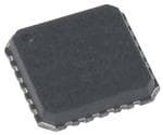
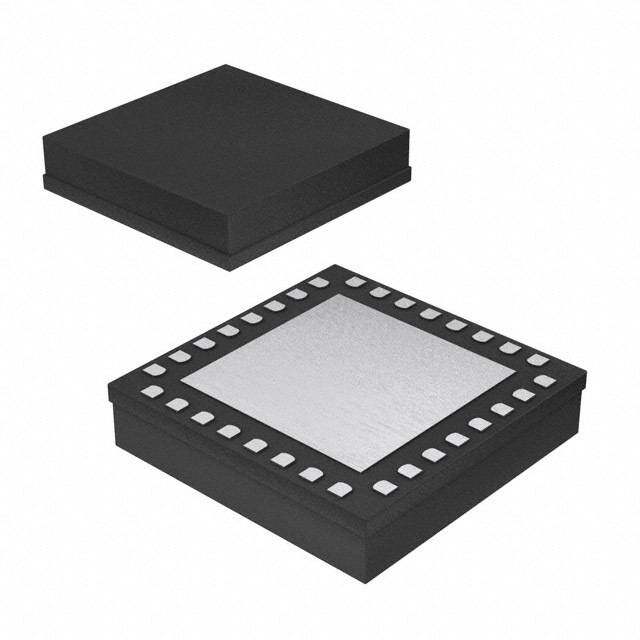
| 产品图片 |
|
| rohs | 符合RoHS无铅 / 符合限制有害物质指令(RoHS)规范要求 |
| 产品系列 | RF集成电路,调节器/解调器,Analog Devices ADL5380ACPZ-R7- |
| 数据手册 | |
| P1dB | 11.6dBm |
| 产品型号 | ADL5380ACPZ-R7 |
| PCN其它 | |
| PCN组件/产地 | |
| RF频率 | 400MHz ~ 6GHz |
| 产品培训模块 | http://www.digikey.cn/PTM/IndividualPTM.page?site=cn&lang=zhs&ptm=24734 |
| 产品目录页面 | |
| 产品种类 | 调节器/解调器 |
| 供应商器件封装 | 24-LFCSP-VQ(4x4) |
| 其它名称 | ADL5380ACPZ-R7DKR |
| 功能 | 解调器 |
| 包装 | Digi-Reel® |
| 商标 | Analog Devices |
| 噪声系数 | 10.9dB |
| 增益 | 6.9dB |
| 安装风格 | SMD/SMT |
| 封装 | Reel |
| 封装/外壳 | 24-VFQFN 裸露焊盘,CSP |
| 封装/箱体 | LFCSP-24 |
| 工作温度范围 | - 40 C to + 85 C |
| 工作电压 | 4.75 V to 5.25 V |
| 工作电流 | 245 mA |
| 工作电源电压 | 4.75 V to 5.25 V |
| 工厂包装数量 | 1500 |
| 接口类型 | LO |
| 最大功率耗散 | 1370 mW |
| 最大工作温度 | + 85 C |
| 最小工作温度 | - 40 C |
| 标准包装 | 1 |
| 电压-电源 | 4.75 V ~ 5.25 V |
| 电流-电源 | 245mA |
| 电源电流 | 245 mA |
| 类型 | Demodulator |
| 系列 | ADL5380 |
| 视频文件 | http://www.digikey.cn/classic/video.aspx?PlayerID=1364138032001&width=640&height=505&videoID=2245193150001 |
| 调制类型 | Quadrature |


- 商务部:美国ITC正式对集成电路等产品启动337调查
- 曝三星4nm工艺存在良率问题 高通将骁龙8 Gen1或转产台积电
- 太阳诱电将投资9.5亿元在常州建新厂生产MLCC 预计2023年完工
- 英特尔发布欧洲新工厂建设计划 深化IDM 2.0 战略
- 台积电先进制程称霸业界 有大客户加持明年业绩稳了
- 达到5530亿美元!SIA预计今年全球半导体销售额将创下新高
- 英特尔拟将自动驾驶子公司Mobileye上市 估值或超500亿美元
- 三星加码芯片和SET,合并消费电子和移动部门,撤换高东真等 CEO
- 三星电子宣布重大人事变动 还合并消费电子和移动部门
- 海关总署:前11个月进口集成电路产品价值2.52万亿元 增长14.8%


PDF Datasheet 数据手册内容提取
400 MHz to 6 GHz Quadrature Demodulator Data Sheet ADL5380 FEATURES FUNCTIONAL BLOCK DIAGRAM Operating RF and LO frequency: 400 MHz to 6 GHz ENBL ADJ Input IP3 ADL5380 IHI 30 dBm at 900 MHz BIAS 28 dBm at 1900 MHz Input IP2: >65 dBm at 900 MHz ILO Input P1dB (IP1dB): 11.6 dBm at 900 MHz Noise figure (NF) LOIP 10.9 dB at 900 MHz RFIN 11.7 dB at 1900 MHz V2I PHQAUSAED RSAPLTIUTRTEER Voltage conversion gain: ~7 dB RFIP LOIN Quadrature demodulation accuracy at 900 MHz Phase accuracy: ~0.2° QHI Amplitude balance: ~0.07 dB Demodulation bandwidth: ~390 MHz BSiansgelbea 5n Vd sI/uQp dprlyiv e: 2 V p-p into 200 Ω QLO 07585-001 Figure 1. APPLICATIONS Cellular W-CDMA/GSM/LTE Microwave point-to-(multi)point radios Broadband wireless and WiMAX GENERAL DESCRIPTION The ADL5380 is a broadband quadrature I-Q demodulator that The fully balanced design minimizes effects from second-order covers an RF/IF input frequency range from 400 MHz to 6 GHz. distortion. The leakage from the LO port to the RF port is With a NF = 10.9 dB, IP1dB = 11.6 dBm, and IIP3 = 29.7 dBm at <−50 dBm. Differential dc offsets at the I and Q outputs are 900 MHz, the ADL5380 demodulator offers outstanding dynamic typically <20 mV. Both of these factors contribute to the range suitable for the demanding infrastructure direct-conversion excellent IIP2 specification, which is >65 dBm. requirements. The differential RF inputs provide a well-behaved The ADL5380 operates off a single 4.75 V to 5.25 V supply. The broadband input impedance of 50 Ω and are best driven from a supply current is adjustable by placing an external resistor from 1:1 balun for optimum performance. the ADJ pin to either the positive supply, V, (to increase supply S Excellent demodulation accuracy is achieved with amplitude current and improve IIP3) or to ground (which decreases supply and phase balances of ~0.07 dB and ~0.2°, respectively. The current at the expense of IIP3). demodulated in-phase (I) and quadrature (Q) differential outputs The ADL5380 is fabricated using the Analog Devices, Inc., are fully buffered and provide a voltage conversion gain of ~7 dB. advanced silicon-germanium bipolar process and is available The buffered baseband outputs are capable of driving a 2 V p-p in a 24-lead exposed paddle LFCSP. differential signal into 200 Ω. Rev. B Document Feedback Information furnished by Analog Devices is believed to be accurate and reliable. However, no responsibility is assumed by Analog Devices for its use, nor for any infringements of patents or other One Technology Way, P.O. Box 9106, Norwood, MA 02062-9106, U.S.A. rights of third parties that may result from its use. Specifications subject to change without notice. No license is granted by implication or otherwise under any patent or patent rights of Analog Devices. Tel: 781.329.4700 ©2009–2014 Analog Devices, Inc. All rights reserved. Trademarks and registered trademarks are the property of their respective owners. Technical Support www.analog.com
ADL5380 Data Sheet TABLE OF CONTENTS Features .............................................................................................. 1 LO Interface ................................................................................ 22 Applications ....................................................................................... 1 V-to-I Converter ........................................................................ 22 Functional Block Diagram .............................................................. 1 Mixers .......................................................................................... 22 General Description ......................................................................... 1 Emitter Follower Buffers ........................................................... 22 Revision History ............................................................................... 2 Bias Circuit .................................................................................. 22 Specifications ..................................................................................... 3 Applications Information .............................................................. 23 Absolute Maximum Ratings ............................................................ 5 Basic Connections ...................................................................... 23 ESD Caution .................................................................................. 5 Power Supply ............................................................................... 23 Pin Configuration and Function Descriptions ............................. 6 Local Oscillator and RF Inputs ................................................. 24 Typical Performance Characteristics ............................................. 7 Baseband Outputs ...................................................................... 25 Low Band Operation .................................................................... 7 Error Vector Magnitude (EVM) Performance ........................... 25 Midband Operation ................................................................... 11 Low IF Image Rejection ............................................................. 26 High Band Operation ................................................................ 14 Example Baseband Interface ..................................................... 27 Distributions for f = 900 MHz ............................................... 17 Characterization Setups ................................................................. 31 LO Distributions for f = 1900 MHz ............................................. 18 Evaluation Board ............................................................................ 33 LO Distributions for f = 2700 MHz ............................................. 19 Thermal Grounding and Evaluation Board Layout ............... 35 LO Distributions for f = 3600 MHz ............................................. 20 Outline Dimensions ....................................................................... 36 LO Distributions for f = 5800 MHz ............................................. 21 Ordering Guide .......................................................................... 36 LO Circuit Description ......................................................................... 22 REVISION HISTORY 12/14—Rev. A to Rev. B Changes to Figure 2 and Table 3 ..................................................... 6 Updated Outline Dimensions ....................................................... 36 Changes to Ordering Guide .......................................................... 36 7/13—Rev. 0 to Rev. A Changes to Table 2 ............................................................................ 5 Deleted Local Oscillator (LO) Input Section .............................. 23 Changed RF Input Section to Local Oscillator and RF Inputs Section .............................................................................................. 24 Added Figure 78, Figure 79, and Figure 82, Renumbered Sequentially .............................................................. 24 Added Figure 83 and Figure 84 .................................................... 25 Changes to Evaluation Board Section and Figure 102 .............. 33 Changes to Table 5 and Figure 103 Caption ............................... 34 Deleted Figure 100, Figure 101, and Figure 102 ......................... 34 Updated Outline Dimensions ....................................................... 36 Changes to Ordering Guide .......................................................... 36 7/09—Revision 0: Initial Version Rev. B | Page 2 of 36
Data Sheet ADL5380 SPECIFICATIONS V = 5 V, T = 25°C, f = 900 MHz, f = 4.5 MHz, P = 0 dBm, Z = 50 Ω, unless otherwise noted. Baseband outputs differentially S A LO IF LO O loaded with 450 Ω. Loss of the balun used to drive the RF port was de-embedded from these measurements. Table 1. Parameter Condition Min Typ Max Unit OPERATING CONDITIONS LO and RF Frequency Range 0.4 6 GHz LO INPUT LOIP, LOIN Input Return Loss LO driven differentially through a balun at 900 MHz −10 dB LO Input Level −6 0 +6 dBm I/Q BASEBAND OUTPUTS QHI, QLO, IHI, ILO Voltage Conversion Gain 450 Ω differential load on I and Q outputs at 900 MHz 6.9 dB 200 Ω differential load on I and Q outputs at 900 MHz 5.9 dB Demodulation Bandwidth 1 V p-p signal, 3 dB bandwidth 390 MHz Quadrature Phase Error At 900 MHz 0.2 Degrees I/Q Amplitude Imbalance 0.07 dB Output DC Offset (Differential) 0 dBm LO input at 900 MHz ±10 mV Output Common Mode Dependent on ADJ pin setting V ~ 4 V (set by 1.5 kΩ from ADJ pin to V) V − 2.5 V ADJ S S V ~ 4.8 V (set by 200 Ω from ADJ pin to V) V − 2.8 V ADJ S S V ~ 2.4 V (ADJ pin open) V − 1.2 V ADJ S 0.1 dB Gain Flatness 37 MHz Output Swing Differential 200 Ω load 2 V p-p Peak Output Current Each pin 12 mA POWER SUPPLIES V = VCC1, VCC2, VCC3 S Voltage 4.75 5.25 V Current 1.5 kΩ from ADJ pin to V; ENBL pin low 245 mA S 1.5 kΩ from ADJ pin to V; ENBL pin high 145 mA S ENABLE FUNCTION Pin ENBL Off Isolation −70 dB Turn-On Settling Time ENBL high to low 45 ns Turn-Off Settling Time ENBL low to high 950 ns ENBL High Level (Logic 1) 2.5 V ENBL Low Level (Logic 0) 1.7 V DYNAMIC PERFORMANCE at RF = 900 MHz V ~ 4 V (set by 1.5 kΩ from ADJ pin to V) ADJ S Conversion Gain 6.9 dB Input P1dB 11.6 dBm RF Input Return Loss RFIP, RFIN driven differentially through a balun −19 dB Second-Order Input Intercept (IIP2) −5 dBm each input tone 68 dBm Third-Order Input Intercept (IIP3) −5 dBm each input tone 29.7 dBm LO to RF RFIN, RFIP terminated in 50 Ω −52 dBm RF to LO LOIN, LOIP terminated in 50 Ω −67 dBc IQ Magnitude Imbalance 0.07 dB IQ Phase Imbalance 0.2 Degrees Noise Figure 10.9 dB Noise Figure Under Blocking Conditions With a −5 dBm input interferer 5 MHz away 13.1 dB Rev. B | Page 3 of 36
ADL5380 Data Sheet Parameter Condition Min Typ Max Unit DYNAMIC PERFORMANCE at RF = 1900 MHz V ~ 4 V (set by 1.5 kΩ from ADJ pin to V) ADJ S Conversion Gain 6.8 dB Input P1dB 11.6 dBm RF Input Return Loss RFIP, RFIN driven differentially through a balun −13 dB Second-Order Input Intercept (IIP2) −5 dBm each input tone 61 dBm Third-Order Input Intercept (IIP3) −5 dBm each input tone 27.8 dBm LO to RF RFIN, RFIP terminated in 50 Ω −49 dBm RF to LO LOIN, LOIP terminated in 50 Ω −77 dBc IQ Magnitude Imbalance 0.07 dB IQ Phase Imbalance 0.25 Degrees Noise Figure 11.7 dB Noise Figure Under Blocking Conditions With a −5 dBm input interferer 5 MHz away 14 dB DYNAMIC PERFORMANCE at RF = 2700 MHz V ~ 4 V (set by 1.5 kΩ from ADJ pin to V) ADJ S Conversion Gain 7.4 dB Input P1dB 11 dBm RF Input Return Loss RFIP, RFIN driven differentially through a balun −10 dB Second-Order Input Intercept (IIP2) −5 dBm each input tone 54 dBm Third-Order Input Intercept (IIP3) −5 dBm each input tone 28 dBm LO to RF RFIN, RFIP terminated in 50 Ω −49 dBm RF to LO LOIN, LOIP terminated in 50 Ω −73 dBc IQ Magnitude Imbalance 0.07 dB IQ Phase Imbalance 0.5 Degrees Noise Figure 12.3 dB DYNAMIC PERFORMANCE at RF = 3600 MHz V ~ 4.8 V (set by200 Ω from ADJ pin to V) ADJ S Conversion Gain 6.3 dB Input P1dB 9.6 dBm RF Input Return Loss RFIP, RFIN driven differentially through a balun −11 dB Second-Order Input Intercept (IIP2) −5 dBm each input tone 48 dBm Third-Order Input Intercept (IIP3) −5 dBm each input tone 21 dBm LO to RF RFIN, RFIP terminated in 50 Ω −46 dBm RF to LO LOIN, LOIP terminated in 50 Ω −72 dBc IQ Magnitude Imbalance 0.14 dB IQ Phase Imbalance 1.1 Degrees Noise Figure 14.2 dB Noise Figure Under Blocking Conditions With a −5 dBm input interferer 5 MHz away 16.2 dB DYNAMIC PERFORMANCE at RF = 5800 MHz V ~ 2.4 V (ADJ pin left open) ADJ Conversion Gain 5.8 dB Input P1dB 8.2 dBm RF Input Return Loss RFIP, RFIN driven differentially through a balun −7.5 dB Second-Order Input Intercept (IIP2) −5 dBm each input tone 44 dBm Third-Order Input Intercept (IIP3) −5 dBm each input tone 20.6 dBm LO to RF RFIN, RFIP terminated in 50 Ω −47 dBm RF to LO LOIN, LOIP terminated in 50 Ω −62 dBc IQ Magnitude Imbalance 0.07 dB IQ Phase Imbalance −1.25 Degrees Noise Figure 15.5 dB Noise Figure Under Blocking Conditions With a −5 dBm input interferer 5 MHz away 18.9 dB Rev. B | Page 4 of 36
Data Sheet ADL5380 ABSOLUTE MAXIMUM RATINGS Table 2. Stresses at or above those listed under Absolute Maximum Parameter Rating Ratings may cause permanent damage to the product. This is a Supply Voltage: VCC1, VCC2, VCC3 5.5 V stress rating only; functional operation of the product at these LO Input Power 13 dBm (re: 50 Ω) or any other conditions above those indicated in the operational RF Input Power 15 dBm (re: 50 Ω) section of this specification is not implied. Operation beyond the maximum operating conditions for extended periods may Internal Maximum Power Dissipation 1370 mW affect product reliability. θ 1 53°C/W JA θ 2.5°C/W JC ESD CAUTION Maximum Junction Temperature 150°C Operating Temperature Range −40°C to +85°C Storage Temperature Range −65°C to +125°C 1 Per JDEC standard JESD 51-2. For information on optimizing thermal impedance, see the Thermal Grounding and Evaluation Board Layout section. Rev. B | Page 5 of 36
ADL5380 Data Sheet PIN CONFIGURATION AND FUNCTION DESCRIPTIONS 3CC3DNPIFNIF3DNJD VGRRGA 432109 222221 PIN 1 GND3 1 INDICATOR 18GND3 GND1 2 17GND2 IHI 3 ADL5380 16QHI ILO 4 TOP VIEW 15QLO GND1 5 (Not to Scale) 14GND2 VCC1 6 13VCC2 789011121 LBNE4DNGPIOLNIOL4DNGCN 07585-002 NOTES 1. NC = NO CONNECT. DO NOT CONNECT TO THIS PIN. 2. THE EXPOSED PAD SHOULD BE CONNECTED TO A LOW IMPEDANCE THERMAL AND ELECTRICAL GROUND PLANE. Figure 2. Pin Configuration Table 3. Pin Function Descriptions Pin No. Mnemonic Description 1, 2, 5, 8, 11, 14, GND1, GND2, GND3, GND4 Ground Connect. 17, 18, 20, 23 3, 4, 15, 16 IHI, ILO, QLO, QHI I Channel and Q Channel Mixer Baseband Outputs. These outputs have a 50 Ω differential output impedance (25 Ω per pin). Each output pair can swing 2 V p-p (differential) into a load of 200 Ω. The output 3 dB bandwidth is ~400 MHz. 6, 13, 24 VCC1, VCC2, VCC3 Supply. Positive supply for LO, IF, biasing, and baseband sections. Decouple these pins to the board ground using the appropriate-sized capacitors. 7 ENBL Enable Control. When pulled low, the part is fully enabled; when pulled high, the part is partially powered down and the output is disabled. 9, 10 LOIP, LOIN Local Oscillator Input. Pins must be ac-coupled. A differential drive through a balun is necessary to achieve optimal performance. Recommended balun is the Mini-Circuits® TC1-1-13 for lower frequencies, the Johanson Technology 3600 balun for midband frequencies, and the Johanson Technology 5400 balun for high band frequencies. Balun choice depends on the desired frequency range of operation. 12 NC No Connect. Do not connect to this pin. 19 ADJ A resistor to V that optimizes third-order intercept. For operation <3 GHz, R = 1.5 kΩ. S ADJ For operation from 3 GHz to 4 GHz, R = 200 Ω. For operation >5 GHz, R = open. ADJ ADJ See the Circuit Description section for more details. 21, 22 RFIN, RFIP RF Input. A single-ended 50 Ω signal can be applied differentially to the RF inputs through a 1:1 balun. Recommended balun is the Mini-Circuits TC1-1-13 for lower frequencies, the Johanson Technology 3600 balun for midband frequencies, and the Johanson Technology 5400 balun for high band frequencies. Balun choice depends on the desired frequency range of operation. EP Exposed Pad. The exposed pad should be connected to a low impedance thermal and electrical ground plane. Rev. B | Page 6 of 36
Data Sheet ADL5380 TYPICAL PERFORMANCE CHARACTERISTICS V = 5 V, T = 25°C, LO drive level = 0 dBm, RF input balun loss is de-embedded, unless otherwise noted. S A LOW BAND OPERATION RF = 400 MHz to 3 GHz; Mini-Circuits TC1-1-13 balun on LO and RF inputs, 1.5 kΩ from the ADJ pin to V. S 18 1.0 TA = –40°C 16 TA = +25°C 0.8 TA = +85°C 0.6 dB), IP1dB (dBm) 111204 INPUGT API1NdB MISMATCH (dB)–000...2024 GAIN ( 8 GAIN –0.4 6 –0.6 4 TA = –40°C –0.8 TA = +25°C TA = +85°C 2 –1.0 400 600 800 1000 1200 1400 1600 1800 2000 2200 2400 2600 2800 3000 07585-003 400 600 800 1000 1200 1400 1600 1800 2000 2200 2400 2600 2800 3000 07585-005 LO FREQUENCY (MHz) LO FREQUENCY (MHz) Figure 3. Conversion Gain and Input 1 dB Compression Point (IP1dB) vs. Figure 5. IQ Gain Mismatch vs. LO Frequency LO Frequency 80 2 I CHANNEL Q CHANNEL 1 70 0 B) IIP3, IIP2 (dBm) 456000 INPUT IPI3N (PI UATN DIP 2Q CHANNELS) BAND RESPONSE (d ––––4321 30 SE –5 A B –6 20 TA = –40°C TA = +25°C –7 10 TA = +85°C –8 400 600 800 1000 1200 1400 1600 1800 2000 2200 2400 2600 2800 3000 07585-004 10 BASEBAND FR1E0Q0UENCY (MHz) 100007585-006 LO FREQUENCY (MHz) Figure 4. Input Third-Order Intercept (IIP3) and Figure 6. Normalized IQ Baseband Frequency Response Input Second-Order Intercept Point (IIP2) vs. LO Frequency Rev. B | Page 7 of 36
ADL5380 Data Sheet 18 35 300 TA = –40°C TA = –40°C 17 TA = +25°C TA = +25°C TA = +85°C B)30 TA = +85°C INPUT IP3 280 16 E (d NOISE FIGURE (dB) 1111124135 dBm) AND NOISE FIGUR11220505 CSUURPRPELNYT 222202460000 SUPPLY CURRENT (mA) 10 P3 ( NOISE FIGURE II 5 180 9 8 0 160 400 600 800 1000 1200 1400 1600 1800 2000 2200 2400 2600 2800 3000 07585-007 1.0 1.5 2.0 2.5 VA3D.J0(V) 3.5 4.0 4.5 07585-010 LO FREQUENCY (MHz) Figure 7. Noise Figure vs. LO Frequency Figure 10. IIP3, Noise Figure, and Supply Current vs. VADJ, fLO = 900 MHz 4 25 es) 3 23 e gr 21 De 2 OR ( B)19 E ERR 1 URE(d17 S 0 G15 RE PHA –1 OISE FI13 1920MHz TU TA = –40°C N11 RA –2 TA = +25°C 920MHz AD TA = +85°C 9 QU –3 7 –4 5 400 600 800 1000 1200LO F1400REQ1600UEN1800CY (M2000Hz)2200 2400 2600 2800 300007585-008 –30 –25 RF–2B0LOCKE–1R5INPUT–1P0OWER(–d5Bm) 0 5 07585-011 Figure 8. IQ Quadrature Phase Error vs. LO Frequency Figure 11. Noise Figure vs. Input Blocker Level, fLO = 900 MHz, fLO = 1900 MHz (RF Blocker 5 MHz Offset) 20 75 18 60 E (dB)18 IIP2, I CHANNEL 70 E (dB)16 IIP2, Q CHANNEL 55 UR16 IIP2, Q CHANNEL 65 UR IIP2, I CHANNEL G G14 50 E FI14 60 E FI NOISE FIGURE 1dB (dBm), NOIS11028 NOISIGPE1 AFdIINBGURE 455505 IIP3, IIP2 ( dBm) 1dB (dBm), NOIS11802 IGPA1dINB 344505 IIP3, IIP2 (dBm) B), IP 6 40 B), IP 6 30 d 4 35 d GAIN ( 2 IIP3 30 GAIN ( 4 IIP3 25 0–6 –5 –4 –3 –2 L–O1 LEVE0L (dB1m) 2 3 4 5 625 07585-009 2–6 –5 –4 –3 –2 LO–1 LEVE0L (dB1m) 2 3 4 5 620 07585-012 Figure 9. Conversion Gain, IP1dB, Noise Figure, IIP3, and IIP2 vs. Figure 12. Conversion Gain, IP1dB, Noise Figure, IIP3, and IIP2 vs. LO Level, fLO = 900 MHz LO Level, fLO = 2700 MHz Rev. B | Page 8 of 36
Data Sheet ADL5380 35 0 TA = –40°C dB) 30 TTAA == ++2855°°CC –5 E ( R 25 GU B) SE FI 20 INPUT IP3 SS (d–10 m) AND NOI 15 RETURN LO–15 B 10 d P3 ( NOISE FIGURE –20 II 5 0 –25 1.0 1.5 2.0 2.5 VAD3J.0(V) 3.5 4.0 4.5 07585-013 0.4 0.6 0.8 1.0 1.2RF1 F.4RE1Q.6UEN1.C8Y 2(G.0Hz2).2 2.4 2.6 2.8 3.0 07585-016 Figure 13. IIP3 and Noise Figure vs. VADJ, fLO = 2700 MHz Figure 16. RF Port Return Loss vs. RF Frequency Measured on Characterization Board Through TC1-1-13 Balun 80 –20 70 –30 Bm), IIP2S(dBm) 5600 Bm) ––5400 (dEL 900MHz: GAIN (d dB),IP1dBQ CHANN 3400 9992700000000MMMMHHHHzzz:::z :III PIIGPP122Ad,,I BNIQ C CHHAANNNNEELL LEAKAGE ––7600 (D 2700MHz: IP1dB GAINIAN 20 22770000MMHHzz:: IIIIPP22,, IQ C CHHAANNNNEELL –80 10 –90 01 2 VADJ3(V) 4 07585-014 –1000.4 0.6 0.8 1.0 1.2 L1O.4 FR1.E6QU1E.8NC2Y.0 (GH2.z2) 2.4 2.6 2.8 3.0 07585-017 Figure 14. Conversion Gain, IP1dB, and IIP2 vs. Figure 17. LO-to-RF Leakage vs. LO Frequency VADJ, fLO = 900 MHz, fLO = 2700 MHz 40 90 –20 TA = –40°C 35 TTAA == ++2855°°CC IQ C CHHAANNNNEELL 85 –30 m) 30 80 dB –40 IP1dB, IIP3 (dBm) 122505 IIP3 IIP2 677505 AND Q CHANNELS ( LEAKAGE (dBc) –––765000 10 60 P2, I –80 IP1dB II 5 55 –90 04.5 6.5 8B.5ASEB1A0N.5D FRE1Q2.U5ENCY1 4(.M5Hz) 16.5 18.5 50 07585-015 –1000.4 0.6 0.8 1.0 1.2RF1 F.4RE1Q.6UEN1.C8Y 2(G.0Hz2).2 2.4 2.6 2.8 3.0 07585-018 Figure 15. IP1dB, IIP3, and IIP2 vs. Baseband Frequency Figure 18. RF-to-LO Leakage vs. RF Frequency Rev. B | Page 9 of 36
ADL5380 Data Sheet 0 –2 –4 B) S (d –6 S O L –8 N R U T–10 E R –12 –14 –16 0.4 0.6 0.8 1.0 1.2LO1 F.4RE1Q.6UEN1.C8Y 2(G.0Hz2).2 2.4 2.6 2.8 3.0 07585-019 Figure 19. LO Port Return Loss vs. LO Frequency Measured on Characterization Board Through TC1-1-13 Balun Rev. B | Page 10 of 36
Data Sheet ADL5380 MIDBAND OPERATION RF = 3 GHz to 4 GHz; Johanson Technology 3600BL14M050T balun on LO and RF inputs, 200 Ω from V to V. ADJ S 14 20 60 13 TA = –40°C dB) 18 IIP2, Q CHANNEL 55 12 TTAA == ++2855°°CC URE ( 16 IIP2, I CHANNEL 50 G m) 11 IP1dB FI 14 45 B(dB 10 OISE 12 NOISE FIGURE 40 Bm) d N IP1dB d IP1 9 m), 10 35 P2 ( GAIN(dB), 678 GAIN N (dB), IP1dB (dB 468 GAIIIPN3 223050 IIP3, II 5 AI 2 15 G 43.0 3.1 3.2 3.3LOF3R.4EQU3E.5NCY3(.G6Hz)3.7 3.8 3.9 4.0 07585-020 0–6 –5 –4 –3 –2LO –L1EVEL0 (dBm1) 2 3 4 5 610 07585-023 Figure 20. Conversion Gain and Input 1 dB Compression Point (IP1dB) vs. Figure 23. Conversion Gain, IP1dB, Noise Figure, IIP3, and IIP2 vs. LO Frequency LO Level, fLO = 3600 MHz 80 18 TA = –40°C TA = +25°C 17 70 TA = +85°C INPUT IP2 I CHANNEL 16 Q CHANNEL 60 15 m) dB) P2 (dB 50 GURE(1134 IIP3, II 3400 INPUT IP3 I AND Q CHANNELS NOISE FI1112 TTTAAA === –++428055°°°CCC 10 20 9 103.0 3.1 3.2 3.3LO F3.R4EQU3E.5NCY3 .(6GHz)3.7 3.8 3.9 4.0 07585-021 83.0 3.1 3.2 3.3LOF3R.4EQU3E.5NCY3(.G6Hz)3.7 3.8 3.9 4.0 07585-024 Figure 21. Input Third-Order Intercept (IIP3) and Figure 24. Noise Figure vs. LO Frequency Input Second-Order Intercept Point (IIP2) vs. LO Frequency 1.0 4 00..68 TTTAAA === –++428055°°°CCC grees) 3 TTTAAA === –++428055°°°CCC dB) 0.4 R(De 2 ( O H R 1 C 0.2 R T E MA 0 SE 0 S A AINMI –0.2 REPH–1 G –0.4 TU RA –2 –0.6 AD U Q –3 –0.8 –1.0 –4 3.0 3.2 LO FR3E.Q4UENCY (G3H.6z) 3.8 4.0 07585-022 3.0 3.1 3.2 3.3LO F3.R4EQU3E.5NCY3 .(6GHz)3.7 3.8 3.9 4.007585-025 Figure 22. IQ Gain Mismatch vs. LO Frequency Figure 25. IQ Quadrature Phase Error vs. LO Frequency Rev. B | Page 11 of 36
ADL5380 Data Sheet 30 300 –20 E (dB)25 TTTAAA === –++428055°°°CCC 280 –30 UR INPUT IP3 m) AND NOISE FIG112050 NOISE FIGURE 222246000 CURRENT (mA) LEAKAGE (dBm) –––654000 B d 3 ( IIP 5 200 –70 SUPPLY CURRENT 0 180 –80 1.0 1.5 2.0 2.5 VAD3J.0(V) 3.5 4.0 4.5 07585-026 3.1 3.2 3.3 3L.4O FRE3.Q5UEN3C.6Y (GH3z.7) 3.8 3.9 4.0 07585-029 Figure 26. IIP3, Noise Figure, and Supply Current vs. VADJ, fLO = 3600 MHz Figure 29. LO-to-RF Leakage vs. LO Frequency 25 –20 –30 23 –40 21 URE (dB)19 E (dBc) –50 G G –60 E FI17 AKA OIS LE –70 N 15 –80 13 –90 11–30 –25 –20RFPO–W15ELLEV–E10L(dBm–)5 0 5 07585-027 –1003.1 3.2 3.3 3R.4F FRE3.Q5UEN3C.6Y (GH3z.7) 3.8 3.9 4.0 07585-030 Figure 27. Noise Figure vs. Input Blocker Level, fLO = 3600 MHz Figure 30. RF-to-LO Leakage vs. RF Frequency (RF Blocker 5 MHz Offset) 80 0 70 –2 B(dBm), IIP2NELS(dBm) 456000 OSS (dB) –4 dN 3600MHz: GAIN L –6 (dB),IP1DQ CHA 2300 333666000000MMMHHHzzz::: IIIPIIPP122d,, BIQ C CHHAANNNNEELL RETURN –8 NN AIA GI 10 –10 0 –10 1 2 VADJ3(V) 4 07585-028 –123.1 3.2 3.3 3R.4F FRE3.Q5UEN3C.6Y (GH3z.)7 3.8 3.9 4.0 07585-031 Figure 28. Conversion Gain, IP1dB, and IIP2 vs. VADJ, fLO = 3600 MHz Figure 31. RF Port Return Loss vs. RF Frequency Measured on Characterization Board Through Johanson Technology 3600 Balun Rev. B | Page 12 of 36
Data Sheet ADL5380 0 –5 B)–10 d S ( S O L–15 N R U T RE–20 –25 –303.1 3.2 3.3 3L.O4 FRE3Q.5UEN3C.Y6 (GH3z.)7 3.8 3.9 4.0 07585-032 Figure 32. LO Port Return Loss vs. LO Frequency Measured on Characterization Board Through Johanson Technology 3600 Balun Rev. B | Page 13 of 36
ADL5380 Data Sheet HIGH BAND OPERATION RF = 5 GHz to 6 GHz; Johanson Technology 5400BL15B050E balun on LO and RF inputs, the ADJ pin is open. 12 20 60 11 dB) 18 NOISE FIGURE 55 m) 10 URE ( 16 IIP2, Q CHANNEL 50 P1dB (dB 89 INPUT P1dB OISE FIG 1124 IIP2, I CHANNEL 4405 Bm) GAIN (dB), INPUT 4567 TTAA == –+4205°°CC GAIN N (dB), IP1dB (dBm), N 10468 GIPIAI1PIdN3B 22330505 IIP3, IIP2 (d 3 TA = +85°C AI 2 15 G 2 0 10 5.1 5.2 5.3 5L.4O FRE5.Q5UEN5C.6Y (GH5z.7) 5.8 5.9 6.0 07585-033 –6 –5 –4 –3 –2LO –L1EVEL0 (dBm1) 2 3 4 5 6 07585-036 Figure 33. Conversion Gain and Input 1 dB Compression Point (IP1dB) vs. Figure 36. Conversion Gain, IP1dB, Noise Figure, IIP3, and IIP2 vs. LO Frequency LO Level, fLO = 5800 MHz 80 20 70 TTTAAA === –++428055°°°CCC IQC CHHAANNNNEELL 1189 TTTAAA === ––+428055°°°CCC 17 60 B) 16 (dBm) 50 INPUTIP2 URE (d 15 2 G 14 IIP3,IIP 3400 INPUTIP3(IANDQ CHANNELS) NOISE FI 1123 11 10 20 9 105.1 5.2 5.3 5L.4OFRE5.Q5UEN5C.6Y(GH5z.7) 5.8 5.9 6.0 07585-034 85.0 5.1 5.2 5.3LO F5.R4EQU5E.5NCY5 (.G6Hz)5.7 5.8 5.9 6.0 07585-037 Figure 34. Input Third-Order Intercept (IIP3) and Figure 37. Noise Figure vs. LO Frequency Input Second-Order Intercept Point (IIP2) vs. LO Frequency 1.0 4 H (dB) 000...468 TTTAAA === –++428055°°°CCC grees) 23 TTTAAA === –++428055°°°CCC C e MAT 0.2 H (D 1 AMPLITUDE MIS ––00..420 PHASE MISMATC ––210 Q –0.6 Q I I –3 –0.8 –1.0 –4 5.1 5.2 5.3 5L.4O FRE5.Q5UEN5C.6Y (GH5z.7) 5.8 5.9 6.0 07585-035 5.1 5.2 5.3 5L.4O FRE5.Q5UEN5C.6Y (GH5z.)7 5.8 5.9 6.0 07585-038 Figure 35. IQ Gain Mismatch vs. LO Frequency Figure 38. IQ Quadrature Phase Error vs. LO Frequency Rev. B | Page 14 of 36
Data Sheet ADL5380 30 300 –20 E (dB)25 INPUT IP3 TTTAAA === ++–428055°°°CCC 280 ––4300 R U m) AND NOISE FIG112050 NOISE FIGURE 222246000 CURRENT (mA) LEAKAGE(dBm) –––765000 B 3 (d SUPPLY CURRENT –80 IIP 5 200 –90 0 180 –100 1.0 1.5 2.0 2.5 VAD3J.0(V) 3.5 4.0 4.5 07585-039 5.1 5.2 5.3 L5O.4FRE5Q.5UEN5C.6Y (GH5.z7) 5.8 5.9 6.0 07585-042 Figure 39. IIP3, Noise Figure, and Supply Current vs. VADJ, fLO = 5800 MHz Figure 42. LO-to-RF Leakage vs. LO Frequency 25 –20 –30 20 –40 B) FIGURE (d15 AGE (dBc) ––5600 E K NOIS10 LEA –70 –80 5 –90 0–30 –25 RF– 2P0OWER LE–V1E5L (dBm)–10 –5 07585-040 –1005.1 5.2 5.3 5R.4F FRE5Q.5UEN5C.Y6 (MH5z.)7 5.8 5.9 6.0 07585-043 Figure 40. Noise Figure vs. Input Blocker Level, fLO = 5800 MHz Figure 43. RF-to-LO Leakage vs. RF Frequency (RF Blocker 5 MHz Offset) 60 0 –2 50 2 m), IIPdBm)40 B) –4 B (dBNEL ( 5800MHz: GAIN SS(d –6 B), IP1dQ CHAN30 555888000000MMMHHHzzz::: IIIPIIPP122d,, BIQ C CHHAANNNNEELL URN LO –8 GAIN (dI AND 20 RET––1120 10 –14 0 –16 1 2 VADJ3 (V) 4 07585-041 5.1 5.2 5.3 RF 5F.4REQU5E.5NCY 5(G.6Hz)5.7 5.8 5.9 6.0 07585-044 Figure 41. Conversion Gain, IP1dB, and IIP2 vs. Figure 44. RF Port Return Loss vs. RF Frequency Measured on RBIAS, fLO = 5800 MHz Characterization Board Through Johanson Technology 5400 Balun Rev. B | Page 15 of 36
ADL5380 Data Sheet –0 –2 –4 B) S (d –6 S O L –8 N R U T–10 E R –12 –14 –16 5.1 5.2 5.3 5L.4O FRE5.Q5UEN5C.6Y (GH5z.7) 5.8 5.9 6.0 07585-045 Figure 45. LO Port Return Loss vs. LO Frequency Measured on Characterization Board Through Johanson Technology 5400 Balun Rev. B | Page 16 of 36
Data Sheet ADL5380 DISTRIBUTIONS FOR f = 900 MHz LO 100 100 90 90 E (%) 80 E(%) 80 TTTAAA === –++428055°°°CCC AG 70 AG 70 NT NT ICHANNEL E 60 E 60 Q CHANNEL C C R R PE 50 PE 50 N N TIO 40 TIO 40 U U RIB 30 RIB 30 DIST 20 TTAA == +–2450°°CC DIST 20 TA = +85°C 10 10 028 29 30 INPUT I3P13 (dBm)32 33 34 07585-046 045 50 55 6I0NPUT I6P52 (dBm7)0 75 80 85 07585-049 Figure 46. IIP3 Distributions Figure 49. IIP2 Distributions for I Channel and Q Channel 100 100 IP1dB 90 90 GAIN %) 80 %) 80 E( E ( AG 70 AG 70 T T N N E 60 E 60 C C R R PE 50 PE 50 N N O 40 O 40 TI TI U U RIB 30 RIB 30 T T DIS 20 TTAA == +–4205°°CC DIS 20 TTAA == –+4205°°CC 10 TA = +85°C 10 TA = +85°C 04 5 6 7GAIN8(dB), I9P1dB1(0dBm)11 12 13 14 07585-047 09.5 10.0 10.N5OISE F1I1G.0URE (dB1)1.5 12.0 12.5 07585-050 Figure 47. Gain and IP1dB Distributions Figure 50. Noise Figure Distributions 100 100 90 90 TA = –40°C E (%) 80 E(%) 80 TTAA == ++2855°°CC AG 70 AG 70 T T N N E 60 E 60 C C R R PE 50 PE 50 N N UTIO 40 UTIO 40 RIB 30 RIB 30 DIST 20 TA = –40°C DIST 20 TA = +25°C 10 TA = +85°C 10 0 0 –0.3 –0.2 –0G.1AINMISM0ATCH(dB0.)1 0.2 0.3 07585-048 –1.0 –0.8 –0Q.6UAD–R0.A4TU–R0E.2PHA0SEER0R.2OR(0D.4egree0s.6) 0.8 1.0 07585-051 Figure 48. IQ Gain Mismatch Distributions Figure 51. IQ Quadrature Phase Error Distributions Rev. B | Page 17 of 36
ADL5380 Data Sheet DISTRIBUTIONS FOR f = 1900 MHz LO 100 100 TA = –40°C 90 90 TA = +25°C %) 80 %) 80 TA = +85°C TAGE( 70 TAGE ( 70 IQ C CHHAANNNNEELL N N E 60 E 60 C C R R PE 50 PE 50 N N TIO 40 TIO 40 U U RIB 30 RIB 30 T T DIS 20 TA = –40°C DIS 20 TA = +25°C 10 TA = +85°C 10 024 25 26 2I7NPUTI2P83(dBm2)9 30 31 32 07585-052 045 50 55 INP6U0T IP2 (d65Bm) 70 75 80 07585-055 Figure 52. IIP3 Distributions Figure 55. IIP2 Distributions for I Channel and Q Channel 100 100 TA = –40°C 90 TA = +25°C 90 %) 80 TA = +85°C %) 80 AGE( 70 IGPA1IdNB AGE ( 70 T T N N E 60 E 60 C C R R PE 50 PE 50 N N TIO 40 TIO 40 U U RIB 30 RIB 30 T T DIS 20 DIS 20 TA = –40°C TA = +25°C 10 10 TA = +85°C 04 5 6 7GAIN8(dB), I9P1dB1(0dBm)11 12 13 14 07585-053 010.5 11.0 11.N5OISE F1I2G.0URE (dB1)2.5 13.0 13.5 07585-056 Figure 53. Gain and IP1dB Distributions Figure 56. Noise Figure Distributions 100 100 90 TA = –40°C 90 TA = –40°C E(%) 80 TTAA == ++2855°°CC E (%) 80 TTAA == ++2855°°CC AG 70 AG 70 NT NT E 60 E 60 C C R R PE 50 PE 50 N N UTIO 40 UTIO 40 RIB 30 RIB 30 DIST 20 DIST 20 10 10 0 0 –0.3 –0.2 –0G.1AINMISM0ATCH(dB0.)1 0.2 0.3 07585-054 –1.0 –0.8 –Q0U.6AD–R0A.4TUR–0E. 2PHAS0E ER0R.2OR (0D.4egree0s.6) 0.8 1.0 07585-057 Figure 54. IQ Gain Mismatch Distributions Figure 57. IQ Quadrature Phase Error Distributions Rev. B | Page 18 of 36
Data Sheet ADL5380 DISTRIBUTIONS FOR f = 2700 MHz LO 100 100 90 90 TA = –40°C I CHANNEL E (%) 80 E (%) 80 TTAA == ++2855°°CC Q CHANNEL AG 70 AG 70 T T EN 60 EN 60 C C R R PE 50 PE 50 N N UTIO 40 TTAA == –+4205°°CC UTIO 40 RIB 30 TA = +85°C RIB 30 T T DIS 20 DIS 20 10 10 0 0 18 20 22 24INPU26T IP3 2(d8Bm)30 32 34 36 07585-058 35 40 45 5I0NPUT I5P52 (dBm6)0 65 70 75 07585-061 Figure 58. IIP3 Distributions Figure 61. IIP2 Distributions for I Channel and Q Channel 100 100 IP1dB TA = –40°C 90 TA = –40°C GAIN 90 TA = +25°C E (%) 80 TTAA == ++2855°°CC E (%) 80 TA = +85°C AG 70 AG 70 T T N N E 60 E 60 C C R R PE 50 PE 50 N N TIO 40 TIO 40 U U RIB 30 RIB 30 T T DIS 20 DIS 20 10 10 0 0 4 5 6 7GAIN8 (dB), I9P1dB1 (0dBm)11 12 13 14 07585-059 10.5 11.0 11.5 NOI1S2E.0 FIGUR12E. 5(dB) 13.0 13.5 14.0 07585-062 Figure 59. Gain and IP1dB Distributions Figure 62. Noise Figure Distributions 100 100 90 90 TA = –40°C E (%) 80 E (%) 80 TTAA == ++2855°°CC AG 70 AG 70 CENT 60 CENT 60 R R PE 50 PE 50 N N UTIO 40 UTIO 40 RIB 30 RIB 30 DIST 20 TA = –40°C DIST 20 TA = +25°C 10 TA = +85°C 10 0 0 –0.3 –0.2 –0G.1AIN MISM0ATCH (dB0.)1 0.2 0.3 07585-060 –2.0 –1.5QU–A1D.0RATU–R0.E5 PHAS0E ERRO0.R5 (Deg1r.e0es) 1.5 2.0 07585-063 Figure 60. IQ Gain Mismatch Distributions Figure 63. IQ Quadrature Phase Error Distributions Rev. B | Page 19 of 36
ADL5380 Data Sheet DISTRIBUTIONS FOR f = 3600 MHz LO 100 100 %) 8900 (%) 8900 TTTAAA === –++428055°°°CCC IQ C CHHAANNNNEELL GE ( 70 AGE 70 CENTA 60 TTAA == –+4205°°CC RCENT 60 ER 50 TA = +85°C PE 50 P N N 40 O 40 O TI BUTI 30 RIBU 30 RI T ST 20 DIS 20 DI 10 10 0 0 15 17 19 21 INPU23T IP3 2(d5Bm)27 29 31 33 07585-064 35 40 45 INP5U0TIP2(d5B5m) 60 65 70 07585-067 Figure 64. IIP3 Distributions Figure 67. IIP2 Distributions for I Channel and Q Channel 100 100 IP1dB TA = –40°C 90 GAIN 90 TA = +25°C PERCENTAGE(%) 56780000 TTTAAA === –++428055°°°CCC PERCENTAGE (%) 56780000 TA = +85°C DISTRIBUTION 234000 DISTRIBUTION 234000 10 10 0 4 5 6 7GAIN8(dB), I9P1dB1(0dBm)11 12 13 14 07585-065 012.5 13.0 13.5 NOI1S4E.0 FIGUR14E. 5(dB) 15.0 15.5 16.0 07585-068 Figure 65. Gain and IP1dB Distributions Figure 68. Noise Figure Distributions 100 100 90 90 TA = –40°C PERCENTAGE(%) 56780000 TTTAAA === –++428055°°°CCC PERCENTAGE(%) 56780000 TTAA == ++2855°°CC DISTRIBUTION 234000 DISTRIBUTION 234000 10 10 0–0.3 –0.2 –0G.1AINMISM0ATCH(dB0.)1 0.2 0.3 07585-066 0–0.5 0QUADRA0T.5UREPHA1S.0EERROR1.5(Degrees2).0 2.5 07585-069 Figure 66. IQ Gain Mismatch Distributions Figure 69. IQ Quadrature Phase Error Distributions Rev. B | Page 20 of 36
Data Sheet ADL5380 DISTRIBUTIONS FOR f = 5800 MHz LO 100 100 90 TA = –40°C 90 TA = –40°C I CHANNEL E (%) 80 TTAA == ++2855°°CC E (%) 80 TTAA == ++2855°°CC Q CHANNEL AG 70 AG 70 T T N N E 60 E 60 C C R R PE 50 PE 50 N N TIO 40 TIO 40 U U RIB 30 RIB 30 T T DIS 20 DIS 20 10 10 018 19 20 INPUT I2P13 (dBm)22 23 24 07585-070 030 35 40 4I5NPUTI5P02(dBm5)5 60 65 70 07585-073 Figure 70. IIP3 Distributions Figure 73. IIP2 Distributions for I Channel and Q Channel 100 100 TA = –40°C 90 TA = +25°C 90 TA = –40°C AGE (%) 7800 TA =IG P+A18dI5NB°C AGE(%) 7800 TTAA == ++2855°°CC T T N N E 60 E 60 C C R R PE 50 PE 50 N N TIO 40 TIO 40 U U RIB 30 RIB 30 T T DIS 20 DIS 20 10 10 0 0 2 3 4 GAI5N (dB), I6P1dB (d7Bm) 8 9 10 07585-071 13.0 13.5 14.0 14.5N1O5I.S0E F1I5G.5UR1E6(.d0B)16.5 17.0 17.5 18.0 07585-074 Figure 71. Gain and IP1dB Distributions Figure 74. Noise Figure Distributions 100 100 TA = –40°C 90 TA = –40°C 90 TA = +25°C (%) 80 TTAA == ++2855°°CC E (%) 80 TA = +85°C GE 70 AG 70 A T T N N 60 E 60 E C C R ER 50 PE 50 P N TION 40 UTIO 40 RIBU 30 TRIB 30 DIST 20 DIS 20 10 10 0 0 –0.3 –0.2 –0.G1AINMISM0ATCH(dB0.)1 0.2 0.3 07585-072 –3 –2QUADRA–T1URE PHAS0E ERROR1 (Degrees)2 3 07585-075 Figure 72. IQ Gain Mismatch Distributions Figure 75. IQ Quadrature Phase Error Distributions Rev. B | Page 21 of 36
ADL5380 Data Sheet CIRCUIT DESCRIPTION The ADL5380 can be divided into five sections: the local Table 4. ADJ Pin Resistor Values and Approximate ADJ Pin oscillator (LO) interface, the RF voltage-to-current (V-to-I) Voltages converter, the mixers, the differential emitter follower outputs, ~ Baseband Common- and the bias circuit. A detailed block diagram of the device is R ~V (V) Mode Output (V) ADJ ADJ shown in Figure 76. 200 Ω to V 4.8 2.2 S ENBL ADJ 600 Ω to V 4.5 2.3 S 1.54 kΩ to V 4 2.5 ADL5380 S IHI BIAS 3.8 kΩ to VS 3.5 2.7 10 kΩ to V 3 3 S Open 2.5 3.2 ILO 9 kΩ to GND 2 3.4 3.5 kΩ to GND 1.5 3.6 LOIP 1.5 kΩ to GND 1 3.8 RFIN QUADRATURE V2I PHASE SPLITTER MIXERS RFIP LOIN The ADL5380 has two double-balanced mixers: one for the in- QHI phase channel (I channel) and one for the quadrature channel (Q channel). These mixers are based on the Gilbert cell design of four cross-connected transistors. The output currents from QLO 07585-076 tthhee ntw feoe dm iinxteor st haree s suubmsemqueedn tto egmetihtteerr i fno ltlhoew reers ibsutifvfee rlso. ads that Figure 76. Block Diagram EMITTER FOLLOWER BUFFERS The LO interface generates two LO signals at 90° of phase The output emitter followers drive the differential I and Q signals difference to drive two mixers in quadrature. RF signals are off chip. The output impedance is set by on-chip 25 Ω series converted into currents by the V-to-I converters that feed into resistors that yield a 50 Ω differential output impedance for the two mixers. The differential I and Q outputs of the mixers each baseband port. The fixed output impedance forms a are buffered via emitter followers. Reference currents to each voltage divider with the load impedance that reduces the effective section are generated by the bias circuit. A detailed description gain. For example, a 500 Ω differential load has 1 dB lower of each section follows. effective gain than a high (10 kΩ) differential load impedance. LO INTERFACE BIAS CIRCUIT The LO interface consists of a polyphase quadrature splitter A band gap reference circuit generates the reference currents followed by a limiting amplifier. The LO input impedance is set used by different sections. The bias circuit can be enabled and by the polyphase, which splits the LO signal into two differential partially disabled using ENBL (Pin 7). If ENBL is grounded or signals in quadrature. The LO input impedance is nominally left open, the part is fully enabled. Pulling ENBL high shuts off 50 Ω. Each quadrature LO signal then passes through a limiting certain sections of the bias circuitry, reducing the standing amplifier that provides the mixer with a limited drive signal. For power to about half of its fully enabled consumption and optimal performance, the LO inputs must be driven differentially. disabling the outputs. V-TO-I CONVERTER The differential RF input signal is applied to a V-to-I converter that converts the differential input voltage to output currents. The V-to-I converter provides a differential 50 Ω input impedance. The V-to-I bias current can be adjusted up or down using the ADJ pin (Pin 19). Adjusting the current up improves IIP3 and IP1dB but degrades SSB NF. Adjusting the current down improves SSB NF but degrades IIP3 and IP1dB. The current adjustment can be made by connecting a resistor from the ADJ pin (Pin 19) to V to increase the bias current or to ground to decrease the S bias current. Table 4 approximately dictates the relationship between the resistor used (R ), the resulting ADJ pin voltage, ADJ and the resulting baseband common-mode output voltage. Rev. B | Page 22 of 36
Data Sheet ADL5380 APPLICATIONS INFORMATION BASIC CONNECTIONS electrical impedance ground plane. If the ground plane spans multiple layers on the circuit board, these layers should be stitched Figure 77 shows the basic connections schematic for the ADL5380. together with nine vias under the exposed paddle. The AN-772 POWER SUPPLY Application Note discusses the thermal and electrical grounding of The nominal voltage supply for the ADL5380 is 5 V and is the LFCSP in detail. Decouple each of the supply pins using two applied to the VCC1, VCC2, and VCC3 pins. Connect ground capacitors; recommended capacitor values are 100 pF and 0.1 µF. to the GND1, GND2, GND3, and GND4 pins. Solder the exposed paddle on the underside of the package to a low thermal and RFIN BALUN 100pF 100pF RADJ VS VS 0.1µF 100pF 24 23 22 21 20 19 3 3 P N 3 J VCC GND RFI RFI GND AD 1GND3 GND3 18 2GND1 GND2 17 IHI 3IHI QHI 16 QHI ADL5380 4ILO QLO 15 ILO QLO 5GND1 GND2 14 V0S.1µF 100pF 6VCC1ENBL GND4 LOIP LOIN GND4 VNCCC2 13 100pF 0.1VµSF 7 8 9 10 11 12 100pF 100pF BALUN LO_SE 07585-078 Figure 77. Basic Connections Schematic Rev. B | Page 23 of 36
ADL5380 Data Sheet LOCAL OSCILLATOR AND RF INPUTS LO INPUT 9 LOIP The RF and LO inputs have a differential input impedance of BALUN 100pF approximately 50 Ω as shown in Figure 78. Figure 79 shows the 10 LOIN return loss. For optimum performance, both the LO and RF ports 100pF 07585-077 should be ac-coupled and driven differentially through a balun as Figure 80. Differential LO Drive shown in Figure 80 and Figure 81. The user has many different types of balun to choose from and from a variety of manufacturers. 21 RFIN For the data presented in this data sheet all measurements were 100pF gathered with the baluns listed below. For applications that are BALUN band specific, the recommended baluns are: 100pF 22 RFIP Up to 3 GHz is the Mini-Circuits TC1-1-13. RF INPUT F36ro0m0B 3L 1G4HMz0 t5o0 4. GHz is the Johanson Technology 07585-079 Figure 81. RF Input From 4.9 GHz to 6 GHz is the Johanson Technology 5400BL15B050. Alternatively, if the single-ended drive of both the LO and RF ports is the desired mode of operation, degradations in IIP2 will be For wideband applications covering the entire 400 MHz to 6 GHz observed because of the lack of common mode rejection. The range of the ADL5380, the recommended balun is the TCM1- degradation in IIP2 is more prevalent at high frequencies, 63AX+ from Mini-Circuits. This wide and maximally flat balun specifically frequencies greater than 1600 MHz. At low frequencies, allows coverage of the entire frequency range with one component. the ADL5380 has inherent common mode rejection offering The recommended drive level for the LO port is between −6 dBm superior IIP2 performance in the 70 dBm range. As shown in and +6 dBm. Figure 82 and Figure 83, in single-ended mode, the largest 120 2.0 performance impact is seen in IIP2 while minimal performance degradation is observed in IIP3. 1.5 100 100 F) CAPACITANCE 1.0 E (p 90 EL R (Ω)IN 8600 00.5 PACITANC 8700 RF AND LO POTRCTMS 1D-6IF3FAEXR+ENITAL DRIVE: L A PARAL 40 RESISTANCE –0.5 ALLEL C 2 (dBm) 6500 –1.0 AR IIP 40 P 20 –1.5 30 RF AND LO PORTS SINGLE-ENDED DRIVE 20 0 –2.0 400 1400 24R0F0 FREQ3U4E0N0CY (M4H4z0)0 5400 6400 07585-178 10 –8 Figure 78. Differential Input Impedance of the RF Port 0400 1400 24F0R0EQUEN3C4Y00 (MHz) 4400 5400 07585-179 B) –10 Figure 82. IIP2 vs. Frequency Comparison for Single-Ended and Differential RT (d –12 Drive of the RF and LO Ports O F P –14 R S –16 S O N L –18 R U –20 T E R –22 L A TI –24 N E R –26 E F F –28 DI –300 0.5 1.0 1.5 2R.0F F2R.E5QU3E.0NCY3. 5(GH4z.)0 4.5 5.0 5.5 6.0 07585-080 Figure 79. Differential RF Port Return Loss Rev. B | Page 24 of 36
Data Sheet ADL5380 40 ERROR VECTOR MAGNITUDE (EVM) PERFORMANCE 35 RF AND LO PORTS DIFFERENITAL EVM is a measure used to quantify the performance of a digital DRIVE: TCM1-63AX+ radio transmitter or receiver. A signal received by a receiver has all 30 constellation points at their ideal locations; however, various 25 imperfections in the implementation (such as magnitude m) B imbalance, noise floor, and phase imbalance) cause the actual d 20 RF AND LO PORTS SINGLE-ENDED DRIVE 3 ( constellation points to deviate from their ideal locations. P II 15 In general, a demodulator exhibits three distinct EVM limitations 10 vs. received input signal power. At strong signal levels, the distortion components falling in-band due to nonlinearities in 5 the device cause strong degradation to EVM as signal levels 0 increase. At medium signal levels, where the demodulator behaves 400 1400 24F0R0EQUEN3C4Y00 (MHz) 4400 5400 07585-180 icno nat lriinbeuatrio mnsa,n tnheer E aVndM t hhea ss iag nteanl dise nwceyll t aob roevaec ha nayn noopttaibmleu mno ise Figure 83. IIP3 vs. Frequency Comparison for Single-Ended and Differential Drive of the RF and LO Ports level determined dominantly by the quadrature accuracy of the demodulator and the precision of the test equipment. As signal To configure the ADL5380 for single-ended drive, terminate the levels decrease, such that noise is a major contribution, the EVM unused input with a 100 pF capacitor to GND while driving the performance vs. the signal level exhibits a decibel-for-decibel alternative input. The single-ended input impedance is 25 Ω or degradation with decreasing signal level. At lower signal levels, half the differential impedance. As a result of this, ensure that where noise proves to be the dominant limitation, the decibel there is proper impedance matching when interfacing with the EVM proves to be directly proportional to the SNR. ADL5380 in single-ended mode for maximum transfer of power. Figure 84, shows an example single ended configuration The ADL5380 shows excellent EVM performance for various when using a signal source with a 50 Ω source impedance. modulation schemes. Figure 86 shows the EVM performance of the ADL5380 with a 16 QAM, 200 kHz low IF. IHI 0 ILO 25Ω RFIP LOIP 25Ω –5 0° –10 RFIN 90° LOIN –15 100pF 100pF QQHLOI 07585-181 EVM (dB) ––2250 Figure 84. Single-Ended Configuration –30 BASEBAND OUTPUTS –35 –40 The baseband outputs QHI, QLO, IHI, and ILO are fixed impedance ports. Each baseband pair has a 50 Ω differential –45 olouatdpsu ta ism lopwed aasn 2ce0.0 T Ωhe ( wouitthpu stos mcaen d beeg praredsaetniotend i wn igthai dni)f foerr ehnitgiahl –50–90 –70 RF I–N5P0UT POWE–R3 0(dBm) –10 10 07585-082 impedance differential loads (500 Ω or greater impedance yields Figure 86. EVM, RF = 900 MHz, IF = 200 kHz vs. RF Input Power for a 16 QAM 160ksym/s Signal the same excellent linearity) that is typical of an ADC. The TCM9-1 9:1 balun converts the differential IF output to a single- ended output. When loaded with 50 Ω, this balun presents a 450 Ω load to the device. The typical maximum linear voltage swing for these outputs is 2 V p-p differential. The output 3 dB bandwidth is 390 MHz. Figure 85 shows the baseband output configuration. IHI 3 16 QHI ADL5380 ILO 4 15 QLO 07585-081 Figure 85. Baseband Output Configuration Rev. B | Page 25 of 36
ADL5380 Data Sheet Figure 87 shows the zero-IF EVM performance of a 10 MHz –10 IEEE 802.16e WiMAX signal through the ADL5380. The –15 differential dc offsets on the ADL5380 are in the order of a few millivolts. However, ac coupling the baseband outputs with 10 µF –20 capacitors eliminates dc offsets and enhances EVM performance. With a 10 MHz BW signal, 10 µF ac coupling capacitors with B)–25 d the 500 Ω differential load results in a high-pass corner frequency M ( V E–30 of ~64 Hz, which absorbs an insignificant amount of modulated 0Hz IF signal energy from the baseband signal. By using ac coupling –35 capacitors at the baseband outputs, the dc offset effects, which 2.5MHz LOW-IF 5MHz LOW-IF can limit dynamic range at low input power levels, can be –40 eliminated. 7.5MHz LOW-IF 0 –45–80 –70 –60 –R5F0 INP–U4T0 POW–3E0R (d–B2m0) –10 0 10 07585-084 Figure 88. EVM, RF = 1900 MHz, IF = 0 Hz, IF = 2.5 MHz, IF = 5 MHz, and IF = –10 7.5 MHz vs. RF Input Power for a W-CDMA Signal (AC-Coupled Baseband Outputs) –20 LOW IF IMAGE REJECTION B) The image rejection ratio is the ratio of the intermediate d M (–30 frequency (IF) signal level produced by the desired input V E 5.8GHz frequency to that produced by the image frequency. The image –40 rejection ratio is expressed in decibels. Appropriate image rejection 3.5GHz is critical because the image power can be much higher than –50 that of the desired signal, thereby plaguing the down-conversion 2.6GHz process. Figure 89 illustrates the image problem. If the upper –60–75 –65 –55 R–F4 5INPU–T3 P5OWE–R25 (dBm–)15 –5 5 07585-083 scihdaenbnaenl d( I( lcohwaenrn seidl)e cbaanncde)l sis t thhee idmesaigree da tb tahned ,l oaw 9e0r° sshidifetb taon tdh e Q Figure 87. EVM, RF = 2.6 GHz, RF = 3.5 GHz, and RF = 5.8 GHz, IF = 0 Hz vs. (upper sideband). Phase and gain balance between I and Q RF Input Power for a 16 QAM 10 MHz Bandwidth Mobile WiMAX Signal channels are critical for high levels of image rejection. (AC-Coupled Baseband Outputs) Figure 88 exhibits multiple W-CDMA low-IF EVM performance curves over a wide RF input power range into the ADL5380. In the case of zero-IF, the noise contribution by the vector signal analyzer becomes predominant at lower power levels, making it difficult to measure SNR accurately. COSωLOt 0° ωIF ωIF –ωIF 0 +ωIF –90° 0 +ωIF +90° ωLSB ωLO ωUSB 0° 0 +ωIF –ωIF 0 +ωIF SINωLOt 07585-085 Figure 89. Illustration of the Image Problem Rev. B | Page 26 of 36
Data Sheet ADL5380 Figure 90 and Figure 91 show the excellent image rejection It is necessary to consider the overall source and load impedance capabilities of the ADL5380 for low IF applications, such as presented by the ADL5380 and ADC input when designing the W-CDMA. The ADL5380 exhibits image rejection greater than filter network. The differential baseband output impedance of 45 dB over a broad frequency range. the ADL5380 is 50 Ω. The ADL5380 is designed to drive a high 60 impedance ADC input. It may be desirable to terminate the ADC input down to lower impedance by using a terminating 50 resistor, such as 500 Ω. The terminating resistor helps to better define the input impedance at the ADC input at the cost of a B) 2.5MHz LOW IF ON (d 40 75MMHHzz LLOOWW IIFF sdleigtahitllsy o rne dthuec eedm giattienr -(fsoelel otwhee rC oiructupiut tD loeascdrinipgt ieofnfe scetsc)t.i o n for TI C JE 30 The order and type of filter network depends on the desired high E E R frequency rejection required, pass-band ripple, and group delay. AG 20 Filter design tables provide outlines for various filter types and M I orders, illustrating the normalized inductor and capacitor values 10 for a 1 Hz cutoff frequency and 1 Ω load. After scaling the 0 07585-103 ncuotr-mofafl ifzreeqdu pernoctyo taynpde leoleamd eimntp veadlaunecs eb, yt hthe es earciteusa rle daecstairnecde 400 800 1200 1600 2000 2400 2800 3200 3600 4000 RF FREQUENCY (MHz) elements are halved to realize the final balanced filter network Figure 90. Low Band and Midband Image Rejection vs. RF Frequency for a component values. W-CDMA Signal, IF = 2.5 MHz, 5 MHz, and 7.5 MHz As an example, a second-order Butterworth, low-pass filter design 60 is shown in Figure 92 where the differential load impedance is 500 Ω and the source impedance of the ADL5380 is 50 Ω. The 50 normalized series inductor value for the 10-to-1, load-to-source B) impedance ratio is 0.074 H, and the normalized shunt capacitor N (d 40 is 14.814 F. For a 10.9 MHz cutoff frequency, the single-ended O CTI 2.5MHz LOW IF equivalent circuit consists of a 0.54 μH series inductor followed E 30 5MHz LOW IF EJ 7MHz LOW IF by a 433 pF shunt capacitor. R E AG 20 The balanced configuration is realized as the 0.54 μH inductor M I is split in half to realize the network shown in Figure 92. 1005000 5200 5400 5600 5800 60007585-1040 VS RS= 50Ω CSONINLNONGFR I=LMG E0UA-.E0RL7NIAZ4DTEHEIDODN CN 14.814F RL= 500Ω RF FREQUENCY (MHz) Figure 91. High Band Image Rejection vs. RF Frequency for a W-CDMA Signal, RS= 0.1 fC = 1Hz IF = 2.5 MHz, 5 MHz, and 7.5 MHz RL RS = 50Ω 0.54µH EXAMPLE BASEBAND INTERFACE DENORMALIZED In most direct-conversion receiver designs, it is desirable to VS SEINQGULIVEA-ELNEDNETD 433pF RL= 500Ω select a wanted carrier within a specified band. The desired channel can be demodulated by tuning the LO to the appropriate fC = 10.9MHz carrier frequency. If the desired RF band contains multiple R2S= 25Ω 0.27µH caa lrorwieerrs IoFf finretqerueesnt,c tyh. eT ahdejsaec eandtja ccaernrti ecrasr arrieer as lcsoan d boew pnr coobnlevmeratteidc itfo VS COBNAFLIGAUNRCAETDION 433pF RR2LL== 225500ΩΩ tohveeyrd arriev ela trhgee brealsaetbivaen tdo s tihgen awl adnetteedc tcioarnr iceirr cbueictrayu.s Ae st hae rye scuanlt , it R2S= 25Ω 0.27µH 2 07585-087 is often necessary to insert a filter to provide sufficient rejection Figure 92. Second-Order Butterworth, Low-Pass Filter Design Example of the adjacent carriers. Rev. B | Page 27 of 36
ADL5380 Data Sheet A complete design example is shown in Figure 95. A sixth-order 900 Butterworth differential filter having a 1.9 MHz corner frequency 800 interfaces the output of the ADL5380 to that of an ADC input. 700 The 500 Ω load resistor defines the input impedance of the ADC. The filter adheres to typical direct conversion W-CDMA s)600 a1p dpBli coaft rioejnesc twiohne ries ,d 1e.s9i2r eMd,H anz da,w 2a.7y MfroHmz tahwea cya rfrroiemr I tFh efr ceaqrureienrc IyF, LAY (n500 E frequency, 10 dB of rejection is desired. D400 Figure 93 and Figure 94 show the measured frequency response 300 and group delay of the filter. 200 10 100 B) 5 0 0.2 0.4 0.6FRE0Q.8UEN1C.0Y (MH1.z2) 1.4 1.6 1.8 07585-089 d E ( Figure 94. Sixth-Order Baseband Filter Group Delay S 0 N O P S RE –5 E D U T NI–10 G A M –15 –20 0 0.5 1.0 FRE1Q.5UENCY2 (.M0Hz) 2.5 3.0 3.5 07585-088 Figure 93. Sixth-Order Baseband Filter Response Rev. B | Page 28 of 36
Data Sheet ADL5380 RFIN BALUN 100pF 100pF VS VS 0.1µF 100pF 24 23 22 21 20 19 3 3 P N 3 J 1GND3VCC GND RFI RFI GND GADND318 2GND1 GND217 3IHI QHI16 ADL5380 4ILO QLO15 5GND1 GND214 V0S.1µF 100pF 6VCC1ENBL GND4 LOIP LOIN GND4 VNCCC213 100pF 0.1µVFS 7 8 9 10 11 12 100pF 100pF BALUN LO_SE CAC CAC CAC CAC 10µF 10µF 10µF 10µF 27µH 27µH 27µH 27µH 270pF 270pF 27µH 27µH 27µH 27µH 100pF 100pF 10µH 10µH 10µH 10µH 68pF 68pF 500Ω 500Ω ADCINPUT ADCINPUT 07585-090 Figure 95. Sixth-Order Low-Pass Butterworth, Baseband Filter Schematic Rev. B | Page 29 of 36
ADL5380 Data Sheet Figure 97 and Figure 98 illustrate the magnitude response and As the load impedance of the filter increases, the filter design group delay response of the fourth-order filter, respectively. becomes more challenging in terms of meeting the required rejection and pass band specifications. In the previous W-CDMA 5 example, the 500 Ω load impedance resulted in the design of a 0 sixth-order filter that has relatively large inductor values and small B) –5 capacitor values. If the load impedance is 200 Ω, the filter design E (d becomes much more manageable. Figure 96 shows a fourth-order NS –10 O filter designed for a 10 MHz wide LTE signal. As shown in SP –15 E Figure 96, the resultant inductor and capacitor values become R Y –20 C much more practical with a 200 Ω load. N E U –25 2.2µH 1.5µH Q E FR –30 50Ω 100pF 22pF 200Ω –35 2.2µH 1.5µH 07585-091 –400 5 10 F1R5EQUE2N0CY (MH25z) 30 35 40 07585-092 Figure 97. Fourth-Order Low-Pass LTE Filter Magnitude Response Figure 96. Fourth-Order Low-Pass LTE Filter Schematic 60 50 s)40 n Y ( A L DE30 P OU GR20 10 0 0 5 10 F1R5EQUE2N0CY (MH25z) 30 35 40 07585-093 Figure 98. Fourth-Order Low-Pass LTE Filter Group Delay Response Rev. B | Page 30 of 36
Data Sheet ADL5380 CHARACTERIZATION SETUPS Figure 99 to Figure 101 show the general characterization bench The two setups shown in Figure 99 and Figure 100 were used setups used extensively for the ADL5380. The setup shown in for making NF measurements. Figure 99 shows the setup for Figure 101 was used to do the bulk of the testing and used measuring NF with no blocker signal applied while Figure 100 sinusoidal signals on both the LO and RF inputs. An automated was used to measure NF in the presence of a blocker. For both Agilent VEE program was used to control the equipment over setups, the noise was measured at a baseband frequency of the IEEE bus. This setup was used to measure gain, IP1dB, IIP2, 10 MHz. For the case where a blocker was applied, the output IIP3, I/Q gain match, and quadrature error. The ADL5380 blocker was at a 15 MHz baseband frequency. Note that great characterization board had a 9-to-1 impedance transformer on care must be taken when measuring NF in the presence of a each of the differential baseband ports to do the differential-to- blocker. The RF blocker generator must be filtered to prevent single-ended conversion, which presented a 450 Ω differential load its noise (which increases with increasing generator output power) to each baseband port, when interfaced with 50 Ω test equipment. from swamping the noise contribution of the ADL5380. At least 30 dB of attention at the RF and image frequencies is desired. For all measurements of the ADL5380, the loss of the RF input For example, assume a 915 MHz signal applied to the LO inputs of balun was de-embedded. Due to the wideband nature of the the ADL5380. To obtain a 15 MHz output blocker signal, the RF ADL5380, three different board configurations had to be used to blocker generator is set to 930 MHz and the filters tuned such characterize the product. For low band characterization (400 MHz that there is at least 30 dB of attenuation from the generator at to 3 GHz), the Mini-Circuits TC1-1-13 balun was used on the both the desired RF frequency (925 MHz) and the image RF RF and LO inputs to create differential signals at the device pins. frequency (905 MHz). Finally, the blocker must be removed For midband characterization (3 GHz to 4 GHz), the Johanson from the output (by the 10 MHz low-pass filter) to prevent Technology 3600BL14M050T was used, and for high band the blocker from swamping the analyzer. characterization (5 GHz to 6 GHz), the Johanson Technology 5400BL15B050E balun was used. SNS CONTROL OUTPUT AGILENT N8974A RT NOISE FIGURE ANALYZER O P S N S R1 M RF 50Ω O GND ADL5380 Q FR VPOS CHAR BOARD I HP 6235A LO INPUT POWER SUPPLY D B PA LOFWIL-TPEARSS EEE d I 6 AGILENT 8665B SIGNAL GENERATOR IEEE PC CONTROLLER 07585-095 Figure 99. General Noise Figure Measurement Setup Rev. B | Page 31 of 36
ADL5380 Data Sheet BAND-PASS BAND-REJECT TUNABLE FILTER TUNABLE FILTER R&S SMT03 SIGNAL GENERATOR D A P B 6d R1 R&S FSEA30 50Ω SPECTRUM ANALYZER RF Q GND ADL5380 LOW-PASS VPOS CHAR BOARD 6dB PAD FILTER I HP 6235A LO POWER SUPPLY D A P B d 6 BAND-PASS HP 87405 CAVITY FILTER LOW NOISE PREAMP SIGANGAILL EGNETN 8E6R6A5BTOR 07585-096 Figure 100. Measurement Setup for Noise Figure in the Presence of a Blocker 3dB PAD RF AMPLIFIER RF 3dB PAD IN OUT 3dB PAD VP GND E E AGILENT IE 3dB PAD 11636A R&S SMT06 RF E E E I D A P R&S SMT06 B d 6 RF Q 6dB PAD EE GND ADL5380 SWITCH IE VPOS CHAR BOARD MATRIX I 6dB PAD AGILENT E3631 LO POWER SUPPLY D A P B S IEEE 6d INRPFUT HANNELND B IEEE CA T A AGILENT E8257D PU SIGNAL GENERATOR N I IEEE IEEE PC CONTROLLER SPECRT&RSU MFS AENAA3L0YZER VECTOHRP V8O50L8TAMETER 07585-097 Figure 101. General Characterization Setup Rev. B | Page 32 of 36
Data Sheet ADL5380 EVALUATION BOARD The ADL5380 evaluation board is available. The evaluation board The board can be used for single-ended or differential baseband is populated with the wide band TCM1-63AX+ transformer analysis. The default configuration of the board is for single-ended from Mini-Circuits. This transformer covers the entire baseband analysis. frequency range of the ADL5380 from 400 MHz to 6 GHZ. RFx T3x C5x C12x R19x R23x VPOS VPOS C11x C8x 24 23 22 21 20 19 3 3 P N 3 J VCC GND RFI RFI GND AD 1 GND3 GND3 18 R5x R3x IPx 2 GND1 GND2 17 QPx R17x R16x R14x R18x 3 IHI QHI 16 T4x C16x R7x ADL5380 R6x C15x T2x 4 ILO QLO 15 R15x R13x INx 5 GND1 GND2 14 QNx R4x R10x R12x R2x VPOS 6 VCC1 VCC2 13 VPOS C9x C6x NBL ND4 OIP OIN ND4 C C7x C10x E G L L G N 7 8 9 10 11 12 R9x R1x R11x VPOS C2x C3x C1x C4x P1x T1x VPOS LOPx LONx LO_SE 07585-098 Figure 102. Evaluation Board Schematic Rev. B | Page 33 of 36
ADL5380 Data Sheet Table 5. Evaluation Board Configuration Options Component Description Default Condition VPOSx, GNDx Power Supply and Ground Vector Pins. Not applicable R10x, R12x, Power Supply Decoupling. Shorts or power supply decoupling resistors. R10x, R12x, R19x = 0 Ω (0603) R19x C6x to C11x The capacitors provide the required dc coupling up to 6 GHz. C6x, C7x, C8x = 100 pF (0402), C9x, C10x, C11x = 0.1 µF (0603) P1x, R11x, Device Enable. When connected to V, the device is active. P1x, R9x = DNI, R1x = DNI, S R9x, R1x R11x = 0 Ω R23x Adjust Pin. The resistor value here sets the bias voltage at this pin and optimizes R23x = 1.5 kΩ (0603) third-order distortion. C1x to C5x, AC Coupling Capacitors. These capacitors provide the required ac coupling C1x, C4x = DNI, C12x from 400 MHz to 4 GHz. C2x, C3x, C5x, C12x = 100 pF (0402) R2x to R7x, Single-Ended Baseband Output Path. This is the default configuration of the R2x to R7x = open, R13x to R18x evaluation board. R13x to R18x are populated for appropriate balun interface. R13x to R18x = 0 Ω (0402) R2x to R5x are not populated. Baseband outputs are taken from QHI and IHI. The user can reconfigure the board to use full differential baseband outputs. R2x to R5x provide a means to bypass the 9:1 TCM9-1 transformer to allow for differential base- band outputs. Access the differential baseband signals by populating R2x to R5x with 0 Ω and not populating R13x to R18x. This way the transformer does not need to be removed. The baseband outputs are taken from the SMAs of QHI, QLO, IHI, and ILO. R6x and R7x are provisions for applying a specific differential load across the baseband outputs T2x, T4x IF Output Interface. TCM9-1 converts a differential high impedance IF output to T2x, T4x = TCM9-1, 9:1 (Mini-Circuits) a single-ended output. When loaded with 50 Ω, this balun presents a 450 Ω load to the device. The center tap can be decoupled through a capacitor to ground. C15x, C16x Decoupling Capacitors. C15x and C16x are the decoupling capacitors used to reject C15x, C16x = 0.1 µF (0402) noise on the center tap of the TCM9-1. T1x LO Input Interface. A 1:1 RF balun that converts the single-ended RF input to TCM1-63AX+ differential signal is used. T3x RF Input Interface. A 1:1 RF balun that converts the single-ended RF input to TCM1-63AX+ differential signal is used. 07585-099 Figure 103. Evaluation Board Top Layer Rev. B | Page 34 of 36
Data Sheet ADL5380 12 mil. THERMAL GROUNDING AND EVALUATION BOARD LAYOUT The package for the ADL5380 features an exposed paddle on the 25 mil. 23 mil. underside that should be well soldered to a low thermal and electrical impedance ground plane. This paddle is typically soldered to an exposed opening in the solder mask on the 82 mil. evaluation board. Figure 104 illustrates the dimensions used in the layout of the ADL5380 footprint on the ADL5380 evaluation board (1 mil = 0.0254 mm). Notice the use of nine via holes on the exposed paddle. These 12 mil. ground vias should be connected to all other ground layers on the evaluation board to maximize heat dissipation from the device package. 19.7 mil. 19383..48 mmiill.. 07585-105 Figure 104. Dimensions for Evaluation Board Layout for the ADL5380 Package Under these conditions, the thermal impedance of the ADL5380 was measured to be approximately 30°C/W in still air. Rev. B | Page 35 of 36
ADL5380 Data Sheet OUTLINE DIMENSIONS 4.10 0.30 4.00 SQ 0.25 PIN 1 3.90 0.18 INDICATOR PIN 1 0.50 19 24 INDICATOR BSC 18 1 EXPOSED 2.65 PAD 2.50 SQ 2.45 13 6 0.50 12 7 0.25 MIN TOP VIEW BOTTOM VIEW 0.40 0.30 0.80 FOR PROPER CONNECTION OF 0.75 0.05 MAX THE EXPOSED PAD, REFER TO 0.70 0.02 NOM THE PIN CONFIGURATION AND FUNCTION DESCRIPTIONS COPLANARITY SECTION OF THIS DATA SHEET. 0.08 SEATING PLANE COMPLIANTTOJED0E.2C0 SRTEAFNDARDS MO-220-WGGD. 03-11-2013-A Figure 105. 24-Lead Lead Frame Chip Scale Package [LFCSP_WQ] 4 mm × 4 mm Body, Very Very Thin Quad (CP-24-7) Dimensions shown in millimeters ORDERING GUIDE Model1 Temperature Range Package Description Package Option Ordering Quantity ADL5380ACPZ-R7 −40°C to +85°C 24-Lead LFCSP_WQ CP-24-7 1,500, 7” Tape and Reel ADL5380ACPZ-WP −40°C to +85°C 24-Lead LFCSP_WQ CP-24-7 64, Waffle Pack ADL5380-EVALZ 1 1 Z = RoHS Compliant Part. ©2009–2014 Analog Devices, Inc. All rights reserved. Trademarks and registered trademarks are the property of their respective owners. D07585-0-12/14(B) Rev. B | Page 36 of 36
Mouser Electronics Authorized Distributor Click to View Pricing, Inventory, Delivery & Lifecycle Information: A nalog Devices Inc.: ADL5380ACPZ-R7 ADL5380-EVALZ