ICGOO在线商城 > 射频/IF 和 RFID > RF 解调器 > LTC5585IUF#PBF

 Datasheet下载
- 型号: LTC5585IUF#PBF
- 制造商: LINEAR TECHNOLOGY
- 库位|库存: xxxx|xxxx
- 要求:
| 数量阶梯 | 香港交货 | 国内含税 |
| +xxxx | $xxxx | ¥xxxx |
查看当月历史价格
查看今年历史价格
LTC5585IUF#PBF产品简介:
ICGOO电子元器件商城为您提供LTC5585IUF#PBF由LINEAR TECHNOLOGY设计生产,在icgoo商城现货销售,并且可以通过原厂、代理商等渠道进行代购。 LTC5585IUF#PBF价格参考。LINEAR TECHNOLOGYLTC5585IUF#PBF封装/规格:RF 解调器, RF Demodulator IC 400MHz ~ 4GHz 24-WFQFN Exposed Pad。您可以下载LTC5585IUF#PBF参考资料、Datasheet数据手册功能说明书,资料中有LTC5585IUF#PBF 详细功能的应用电路图电压和使用方法及教程。
LTC5585IUF#PBF 是 Linear Technology(现为 Analog Devices)生产的一款高性能 RF 解调器,属于宽带零中频 (Zero-IF) 解调器系列。其主要应用场景包括:

1. 无线通信系统
   LTC5585 适用于各种无线通信设备,如蜂窝基站、微波回传链路和软件定义无线电 (SDR) 系统。它能够处理宽频率范围内的射频信号,支持多标准通信协议。

2. 雷达与传感器系统
   在雷达和传感器应用中,LTC5585 可用于解调接收到的高频信号,提取目标的距离、速度和角度信息。例如,汽车毫米波雷达或工业监测雷达。

3. 卫星通信与广播接收
   该芯片可用于卫星通信地面站或数字广播接收机中,实现对高频信号的精确解调,确保高质量的数据传输或音频/视频播放。

4. 测试与测量设备
   在射频测试仪器中,LTC5585 能够帮助分析复杂的射频信号特性,例如频谱分析仪、矢量信号分析仪等。

5. 物联网 (IoT) 和低功耗通信
   对于需要高效射频信号处理的 IoT 设备,LTC5585 提供了高集成度和低功耗的解决方案,适合远程传感器网络或智能家居设备。

6. 军事与航空航天领域
   因为其出色的线性度和动态范围性能,LTC5585 还被广泛应用于军用通信、电子战系统以及航天器通信模块中。

总结来说,LTC5585IUF#PBF 的宽带支持能力、高灵敏度和低噪声特性使其成为许多现代射频系统的理想选择,尤其在需要高性能信号处理的场合表现出色。
| 参数 | 数值 |
| 产品目录 | |
| 描述 | IC DEMOD WIDEBAND IQ 3GHZ 24 QFN |
| 产品分类 | |
| LO频率 | 400MHz ~ 4GHz |
| 品牌 | Linear Technology |
| 数据手册 | http://www.linear.com/docs/40950 |
| 产品图片 |
|
| P1dB | 16dBm |
| 产品型号 | LTC5585IUF#PBF |
| RF频率 | 400MHz ~ 4GHz |
| rohs | 无铅 / 符合限制有害物质指令(RoHS)规范要求 |
| 产品系列 | - |
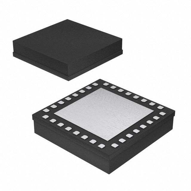
| 供应商器件封装 | 24-QFN(4x4) |
| 其它名称 | LTC5585IUFPBF |
| 功能 | 解调器 |
| 包装 | 管件 |
| 噪声系数 | 13.5dB |
| 增益 | 2.4dB |
| 封装/外壳 | 24-WFQFN 裸露焊盘 |
| 标准包装 | 91 |
| 特色产品 | http://www.digikey.com/product-highlights/cn/zh/linear-technology-ltc5585-demodulator/1622 |
| 电压-电源 | 4.75 V ~ 5.25 V |
| 电流-电源 | 200mA |


- 商务部:美国ITC正式对集成电路等产品启动337调查
- 曝三星4nm工艺存在良率问题 高通将骁龙8 Gen1或转产台积电
- 太阳诱电将投资9.5亿元在常州建新厂生产MLCC 预计2023年完工
- 英特尔发布欧洲新工厂建设计划 深化IDM 2.0 战略
- 台积电先进制程称霸业界 有大客户加持明年业绩稳了
- 达到5530亿美元!SIA预计今年全球半导体销售额将创下新高
- 英特尔拟将自动驾驶子公司Mobileye上市 估值或超500亿美元
- 三星加码芯片和SET,合并消费电子和移动部门,撤换高东真等 CEO
- 三星电子宣布重大人事变动 还合并消费电子和移动部门
- 海关总署:前11个月进口集成电路产品价值2.52万亿元 增长14.8%


PDF Datasheet 数据手册内容提取
LTC5585 Wideband IQ Demodulator with IIP2 and DC Offset Control FEATURES DESCRIPTION n 400MHz to 4GHz Operating Frequency The LTC®5585 is a direct conversion quadrature demodu- n High IIP3: 28.7dBm at 700MHz, 25.7dBm at 1.95GHz lator optimized for high linearity receiver applications in n High IIP2: 70dBm at 700MHz, 60dBm at 1.95GHz the 400MHz to 4GHz frequency range. It is suitable for n User Adjustable IIP2 Up to 80dBm communications receivers where an RF signal is directly n User Adjustable DC Offset Null converted into I and Q baseband signals with bandwidth n High Input P1dB: 16dBm at 1950MHz of 530MHz or higher. The LTC5585 incorporates balanced n I/Q Bandwidth of 530MHz or Higher I and Q mixers, LO buffer amplifiers and a precision, high n Image Rejection: 43dB at 1950MHz frequency quadrature phase shifter. The integrated on-chip n Noise Figure: 13.5dB at 700MHz broadband transformer provides a single-ended interface 12.7dB at 1.95GHz at the RF input with simple off-chip L-C matching. In ad- n Conversion Gain: 2.0dB at 700MHz dition, the LTC5585 provides four analog control voltage 2.4dB at 1.95GHz interface pins for IIP2 and DC offset correction, greatly n Single-Ended RF with On-Chip Transformer simplifying system calibration. n Shutdown Mode The high linearity of the LTC5585 provides excellent spur- n Operating Temperature Range (T ): –40°C to 105°C C free dynamic range for the receiver. This direct conversion n 24-Lead 4mm × 4mm QFN Package demodulator can eliminate the need for intermediate fre- APPLICATIONS quency (IF) signal processing, as well as the corresponding requirements for image filtering and IF filtering. These n LTE/W-CDMA/TD-SCDMA Base Station Receivers I/Q outputs can interface directly to channel-select filters n Wideband DPD Receivers (LPFs) or to baseband amplifiers. n Point-To-Point Broadband Radios L, LT, LTC, LTM, Linear Technology and the Linear logo are registered trademarks of Linear n High Linearity Direct Conversion I/Q Receivers Technology Corporation. All other trademarks are the property of their respective owners. n Image Rejection Receivers TYPICAL APPLICATION Direct Conversion Receiver with IIP2 and DC Offset Calibration 5V BPF LNA BPF INPURTF RF VCC I+ LPF VGA IIP2 vs IP2I, IP2Q Trim Voltage I– A/D 120 I, –40°C Q, –40°C fRF = 700MHz I, 25°C Q, 25°C 110 I, 85°C Q, 85°C IP2 ADJUST D/A I, 105°C Q, 105°C IP2 AND DC 100 OFFSET CAL DC OFFSET D/A m) 90 B LO INPUT LO 0° LTC5585 P2 (d 80 90° II 70 D/A DC OFFSET IP2 AND DC 60 OFFSET CAL IP2 ADJUST 50 D/A 40 Q+ LPF VGA 0 0.1 0.2 0.3 0.4 0.5 0.6 0.7 0.8 0.9 1.0 ENABLE EN Q– A/D IP2I, IP2Q (V) 5585 G09 5585 TA01a 5585fb 1 For more information www.linear.com/LTC5585
LTC5585 ABSOLUTE MAXIMUM RATINGS PIN CONFIGURATION (Note 1) V Supply Voltage ...................................–0.3V to 5.5V TOP VIEW CC VCAP Voltage .................................................VCC ±0.05V REF+I–I+Q–Q CMI I–, I+, Q+, Q–, CMI, CMQ Voltage ........2.5V to V + 0.3V 24 23 22 21 20 19 CC Voltage on Any Other Pin .................–0.3V to V + 0.3V IP2Q 1 18 CMQ CC LO+, LO–, RF Input Power ....................................20dBm DCOQ 2 17 VCAP DCOI 3 25 16 LO– RF Input DC Voltage ...............................................±0.1V IP2I 4 GND 15 LO+ Maximum Junction Temperature (T ) .............150°C JMAX RF 5 14 GND Operating Temperature Range (TC) ........–40°C to 105°C GND 6 13 GND Storage Temperature Range ..................–65°C to 150°C 7 8 9 10 11 12 N D S C C 2 E GN VBIA VC ED EIP UF PACKAGE 24-LEAD (4mm × 4mm) PLASTIC QFN TJMAX = 150°C, θJC = 7°C/W EXPOSED PAD (PIN 25) IS GND, MUST BE SOLDERED TO PCB ORDER INFORMATION LEAD FREE FINISH TAPE AND REEL PART MARKING PACKAGE DESCRIPTION TEMPERATURE RANGE LTC5585IUF#PBF LTC5585IUF#TRPBF 5585 24-Lead (4mm x 4mm) Plastic QFN –40°C to 105°C Consult LTC Marketing for parts specified with wider operating temperature ranges. Consult LTC Marketing for information on non-standard lead based finish parts. For more information on lead free part marking, go to: http://www.linear.com/leadfree/ For more information on tape and reel specifications, go to: http://www.linear.com/tapeandreel/ ELECTRICAL CHARACTERISTICS T = 25°C, V = 5V, EN = 5V, EDC = EIP2 = 0V, REF = IP2I = IP2Q = DCOI = C CC DCOQ = 0.5V, P = –5dBm (–5dBm/tone for 2-tone IIP2 and IIP3 tests), P = 6dBm, unless otherwise noted. (Notes 2, 3, 5, 6, 9) RF LO SYMBOL PARAMETER CONDITIONS MIN TYP MAX UNITS f RF Input Frequency Range (Note 12) 0.4 to 4.0 GHz RF(RANGE) f LO Input Frequency Range (Note 12) 0.4 to 4.0 GHz LO(RANGE) P LO Input Power Range (Note 12) 0 to 10 dBm LO(RANGE) f = 700MHz, f = 701MHz, f = 690MHz, L6 = 2.7pF, C19 = 1.0pF, L5 = 12nH, C14 = 5.6pF RF1 RF2 LO f RF Input Frequency Range Return Loss > 10dB 680 to 870 MHz RF(MATCH) f LO Input Frequency Range Return Loss > 10dB 690 to 820 MHz LO(MATCH) G Voltage Conversion Gain Loaded with 100Ω Pull-Up (Note 8) 2.0 dB V NF Noise Figure Double-Side Band (Note 4) 13.5 dB NF Noise Figure Under Blocking Conditions Double-Side Band, P = 0dBm (Note 7) 15.5 dB BLOCKING RF IIP3 Input 3rd Order Intercept 28.7 dBm IIP2 Input 2nd Order Intercept Unadjusted, EIP2 = 0V 70 dBm IIP2 Optimized Input 2nd Order Intercept EIP2 = 5V, IP2I, IP2Q Adjusted for Minimum IM2 80 dBm OPT P1dB Input 1dB Compression 16 dBm 5585fb 2 For more information www.linear.com/LTC5585
LTC5585 ELECTRICAL CHARACTERISTICS T = 25°C, V = 5V, EN = 5V, EDC = EIP2 = 0V, REF = IP2I = IP2Q = DCOI = C CC DCOQ = 0.5V, P = –5dBm (–5dBm/tone for 2-tone IIP2 and IIP3 tests), P = 6dBm, unless otherwise noted. (Notes 2, 3, 5, 6, 9) RF LO SYMBOL PARAMETER CONDITIONS MIN TYP MAX UNITS DC DC Offset at I/Q Outputs Unadjusted, EDC = 0V (Note 13) 4 mV OFFSET ∆G I/Q Gain Mismatch 0.05 dB ∆φ I/Q Phase Mismatch 0.3 Deg IRR Image Rejection Ratio (Note 10) 48 dB LO-RF LO to RF Leakage –64 dBm RF-LO RF to LO Isolation 60 dB f = 1950MHz, f = 1951MHz, f = 1940MHz, L6 = 1.2pF, C19 = 5.1nH, L5 = 1.0pF, C13 = 5.1nH RF1 RF2 LO f RF Input Frequency Range Return Loss > 10dB 1.6 to 2.1 GHz RF(MATCH) f LO Input Frequency Range Return Loss > 10dB 1.85 to 2.05 GHz LO(MATCH) G Voltage Conversion Gain Loaded with 100Ω Pull-Up (Note 8) 2.4 dB V NF Noise Figure Double-Side Band (Note 4) 12.7 dB IIP3 Input 3rd Order Intercept 25.7 dBm IIP2 Input 2nd Order Intercept Unadjusted, EIP2 = 0V 60 dBm IIP2 Optimized Input 2nd Order Intercept EIP2 = 5V, IP2I, IP2Q Adjusted for Minimum IM2 80 dBm OPT P1dB Input 1dB Compression 16 dBm DC DC Offset at I/Q Outputs Unadjusted, EDC = 0V (Note 13) 7 mV OFFSET ∆G I/Q Gain Mismatch 0.05 dB ∆φ I/Q Phase Mismatch 0.7 Deg IRR Image Rejection Ratio (Note 10) 43 dB LO-RF LO to RF Leakage –49 dBm RF-LO RF to LO Isolation 58 dB f = 2150MHz, f = 2151MHz, f = 2140MHz, C17 = 1.5pF, L6 = 4.7nH, C19 = 0.5pF, L5 = 5.1nH, C14 = 0.7pF RF1 RF2 LO f RF Input Frequency Range Return Loss > 10dB 2.03 to 2.36 GHz RF(MATCH) f LO Input Frequency Range Return Loss > 10dB 2.05 to 2.18 GHz LO(MATCH) G Voltage Conversion Gain Loaded with 100Ω Pull-Up (Note 8) 2.3 dB V NF Noise Figure Double-Side Band (Note 4) 13.0 dB NF Noise Figure Under Blocking Conditions Double-Side Band, P = 0dBm (Note 7) 14.6 dB BLOCKING RF IIP3 Input 3rd Order Intercept 25.9 dBm IIP2 Input 2nd Order Intercept Unadjusted, EIP2 = 0V 56 dBm IIP2 Optimized Input 2nd Order Intercept EIP2 = 5V, IP2I, IP2Q Adjusted for Minimum IM2 80 dBm OPT P1dB Input 1dB Compression 15 dBm DC DC Offset at I/Q Outputs Unadjusted, EDC = 0V (Note 13) 6 mV OFFSET ∆G I/Q Gain Mismatch 0.05 dB ∆φ I/Q Phase Mismatch 1.0 Deg IRR Image Rejection Ratio (Note 10) 40 dB LO-RF LO to RF Leakage –50 dBm RF-LO RF to LO Isolation 60 dB f = 2600MHz, f = 2601MHz, f = 2590MHz, C17 = 0.5pF, L6 = 2.7nH, L5 = 1.2nH, C14 = 1pF RF1 RF2 LO f RF Input Frequency Range Return Loss > 10dB 2.35 to 3.1 GHz RF(MATCH) f LO Input Frequency Range Return Loss > 10dB 2.47 to 2.65 GHz LO(MATCH) G Voltage Conversion Gain Loaded with 100Ω Pull-Up (Note 8) 2.3 dB V 5585fb 3 For more information www.linear.com/LTC5585
LTC5585 ELECTRICAL CHARACTERISTICS T = 25°C, V = 5V, EN = 5V, EDC = EIP2 = 0V, REF = IP2I = IP2Q = DCOI = C CC DCOQ = 0.5V, P = –5dBm (–5dBm/tone for 2-tone IIP2 and IIP3 tests), P = 6dBm, unless otherwise noted. (Notes 2, 3, 5, 6, 9) RF LO SYMBOL PARAMETER CONDITIONS MIN TYP MAX UNITS NF Noise Figure Double-Side Band (Note 4) 13.6 dB NF Noise Figure Under Blocking Conditions Double-Side Band, P = 0dBm (Note 7) 15.2 dB BLOCKING RF IIP3 Input 3rd Order Intercept 27.5 dBm IIP2 Input 2nd Order Intercept Unadjusted, EIP2 = 0V 60 dBm IIP2 Minimum Input 2nd Order Intercept EIP2 = 5V, IP2I, IP2Q Adjusted for Minimum IM2 80 dBm OPT P1dB Input 1dB Compression 15.5 dBm DC DC Offset at I/Q Outputs Unadjusted, EDC = 0V (Note 13) 8 mV OFFSET ∆G I/Q Gain Mismatch 0.05 dB ∆φ I/Q Phase Mismatch 1.0 Deg IRR Image Rejection Ratio (Note 10) 40 dB LO-RF LO to RF Leakage –46 dBm RF-LO RF to LO Isolation 55 dB f = 3500MHz, f = 3501MHz, f = 3490MHz, C17 = 0.6pF, L6 = 1.0nH, C13 = 0.7pF, L5 = Short, C14 = Open, Single-Ended LO (See Figure 14) RF1 RF2 LO f RF Input Frequency Range Return Loss > 10dB 2.88 to 3.97 GHz RF(MATCH) f LO Input Frequency Range Return Loss > 10dB 2.97 to 3.96 GHz LO(MATCH) G Voltage Conversion Gain Loaded with 100Ω Pull-Up (Note 8) 0.3 dB V NF Noise Figure Double-Side Band (Note 4) 17.1 dB IIP3 Input 3rd Order Intercept 28.1 dBm IIP2 Input 2nd Order Intercept Unadjusted, EIP2 = 0V 52.5 dBm IIP2 Minimum Input 2nd Order Intercept EIP2 = 5V, IP2I, IP2Q Adjusted for Minimum IM2 65.9 dBm OPT P1dB Input 1dB Compression 17.1 dBm DC DC Offset at I/Q Outputs Unadjusted, EDC = 0V (Note 13) 16.5 mV OFFSET ∆G I/Q Gain Mismatch 0.04 dB ∆φ I/Q Phase Mismatch 1.8 Deg IRR Image Rejection Ratio (Note 10) 36 dB LO-RF LO to RF Leakage –34.7 dBm RF-LO RF to LO Isolation 44.5 dB Power Supply and Other Parameters V Supply Voltage 4.75 5.0 5.25 V CC I Supply Current EDC = EIP2 = 5V 180 200 220 mA CC I Supply Current EDC = EIP2 = 0V 170 190 210 mA CC(LOW) I Shutdown Current EN < 0.3V 11 900 μA CC(OFF) t Turn-On Time EN Transition from Logic Low to High (Note 14) 0.2 µs ON t Turn-Off Time EN Transition from Logic High to Low (Note 15) 0.8 µs OFF V EN, EDC, EIP2 Input High Voltage (On) 2.0 V EH V EN, EDC, EIP2 Input Low Voltage (Off) 0.3 V EL I EN Pin Input Current EN = 5.0V 52 μA ENH I EDC Pin Input Current EDC = 5.0V 33 μA EDCH 5585fb 4 For more information www.linear.com/LTC5585
LTC5585 ELECTRICAL CHARACTERISTICS SYMBOL PARAMETER CONDITIONS MIN TYP MAX UNITS I EIP2 Pin Input Current EIP2 = 5.0V 50 μA EIP2H V REF Pin Voltage With REF Pin Unloaded 0.5 V REF V REF Pin Voltage Range When Driven with External Source 0.4 to 0.7 V REF(RANGE) Z REF Input Impedance (Note 11) 2||1 kΩ||pF REF DCOI, DCOQ, IP2I, IP2Q Pin Voltage Unloaded 0.5 V DCOI, DCOQ, IP2I, IP2Q Voltage Range When Driven with External Source 0 to 2V V REF DCOI, DCOQ, IP2I, IP2Q Impedance (Note 11) 8||1 kΩ||pF DCOI, DCOQ, IP2I, IP2Q Settling Time For Step Input, Output with 90% of Final Value 20 ns DC Offset Adjustment Range DCOI, DCOQ Swept from 0V to 1V, EDC = 5V ±20 mV DC Offset Drift Over Temperature Unadjusted, EDC = 0V 20 μV/°C V I+, I–, Q+, Q– Common Mode Voltage V – 1.5 V CM CC Z I+, I–, Q+, Q– Output Impedance Single Ended 100||6 Ω||pF OUT BW I+, I–, Q+, Q– Output Bandwidth 100Ω External Pull-Up, –3dB Corner Frequency 530 MHz BB Note 1: Stresses beyond those listed under Absolute Maximum Ratings Note 8: Voltage conversion gain is calculated from the average measured may cause permanent damage to the device. Exposure to any Absolute power conversion gain of the I and Q outputs using the test circuit shown Maximum Rating condition for extended periods may affect device in Figure 1. Power conversion gain is measured with a 100Ω differential reliability and lifetime. load impedance on the I and Q outputs. Note 2: Tests are performed with the test circuit of Figure 1. Note 9: Baseband outputs have a 100Ω external pull-up resistor to V as CC Note 3: The LTC5585 is guaranteed to be functional over the –40°C to shown in the test circuit shown in Figure 1. 105°C case temperature operating range. Note 10: Image rejection is calculated from the measured gain error and Note 4: DSB noise figure is measured at the baseband frequency of 15MHz phase error using the method listed in the appendix. with a small-signal noise source without any filtering on the RF input and Note 11: The DCOI, DCOQ, IP2I, IP2Q pins have an 8k internal resistor to no other RF signal applied. ground. The REF pin has a 2k internal resistor to ground. If unconnected, Note 5: Performance at the RF frequencies listed is measured with external these pins will float up to 500mV through internal current sources. A low RF and LO impedance matching, as shown in the table of Figure 1. output resistance voltage source is recommended for driving these pins. Note 6: The complementary outputs (I+, I– and Q+, Q–) are combined Note 12: This is the recommended operating range, operation outside the using a 180° phase-shift combiner. listed range is possible with degraded performance to some parameters. Note 7: Noise figure under blocking conditions (NF ) is measured Note 13: DC offset measured differentially between I+ and I– and between BLOCKING at an output frequency of 60MHz with RF input signal at f + 1MHz. Both Q+ and Q–. The reported value is the mean of the absolute values of the LO RF and LO input signals are appropriately filtered, as well as the baseband characterization data distribution. output. NFBLOCKING measured at 840MHz, 2140MHz and 2500MHz only. Note 14: Baseband amplitude is within 10% of final value. Note 15: Baseband amplitude is at least 30dB down from its on state. 5585fb 5 For more information www.linear.com/LTC5585
LTC5585 DC PERFORMANCE CHARACTERISTICS EN = 5V, EDC = 0V and EIP2 = 0V. Test circuit shown in Figure 1 Supply Current vs Supply Voltage REF Voltage vs Temperature 260 550 250 TTCC == –2450°C°C 545 VVCCCC == 45.V75V 240 TC = 85°C 540 VCC = 5.25V A) TC = 105°C RENT (m222300 GE (mV)553350 Y CUR220100 VOLTA552205 UPPL190 REF 515 S 180 510 170 505 160 500 4.75 5 5.25 –40 –20 0 20 40 60 80 100 SUPPLY VOLTAGE (V) TEMPERATURE (°C) 5585 G01 5585 G02 TYPICAL PERFORMANCE CHARACTERISTICS 700MHz application. V = 5V, EN = 5V, EDC = 0V, CC EIP2 = 0V, REF = 0.5V, T = 25°C, P = 6dBm, f = 690MHz, f = 700MHz, f = 701MHz, f = 10MHz, P = P = –5dBm, C LO LO RF1 RF2 BB RF1 RF2 DC Blocks and Mini-Circuits PSCJ-2-1 180° combiner at baseband outputs de-embedded from measurement unless otherwise noted. Test circuit with RF and LO ports impedance matched as in Figure 1. IIP3, P1dB vs Temperature (T ) IIP3, P1dB vs Supply Voltage (V ) IIP3 vs LO Power C CC 50 50 50 I, –40°C Q, –40°C I, 4.75V Q, 4.75V TC = 25°C I, 0dBm Q, 0dBm TC = 25°C 46 I, 25°C Q, 25°C 46 I, 5.0V Q, 5.0V 46 I, 6dBm Q, 6dBm I, 85°C Q, 85°C I, 5.25V Q, 5.25V I, 10dBm Q, 10dBm 42 I, 105°C Q, 105°C 42 42 38 38 38 m) m) dB 34 IIP3 dB 34 m) 34 3, P1dB ( 2360 3, P1dB ( 2360 IIP3 IIP3 (dB 2360 P P II 22 II 22 22 18 P1dB 18 P1dB 18 14 14 14 10 10 10 600 700 800 900 1000 600 700 800 900 1000 600 700 800 900 1000 LO FREQUENCY (MHz) LO FREQUENCY (MHz) LO FREQUENCY (MHz) 5585 G03 5585 G04 5585 G05 5585fb 6 For more information www.linear.com/LTC5585
LTC5585 TYPICAL PERFORMANCE CHARACTERISTICS 700MHz application. V = 5V, EN = 5V, EDC = 0V, CC EIP2 = 0V, REF = 0.5V, T = 25°C, P = 6dBm, f = 690MHz, f = 700MHz, f = 701MHz, f = 10MHz, P = P = –5dBm, C LO LO RF1 RF2 BB RF1 RF2 DC Blocks and Mini-Circuits PSCJ-2-1 180° combiner at baseband outputs de-embedded from measurement unless otherwise noted. Test circuit with RF and LO ports impedance matched as in Figure 1. Uncalibrated IIP2 vs Temperature 2-Tone IIP3 vs RF Power (T ) Uncalibrated IIP2 vs LO Power C 50 120 120 48 I, –40°C Q, –40°C fRF1 = 700MHz I, –40°C Q, –40°C I, 0dBm Q, 0dBm TC = 25°C 4446 III,,, 281550°°5CC°C QQQ,,, 281550°°5CC°C ffRLOF2 = = 6 79001MMHHzz 110 III,,, 281550°°5CC°C QQQ,,, 281550°°5CC°C 110 II,, 61d0BdBmm QQ,, 61d0BdBmm 42 100 100 40 dBm) 3386 dBm) 90 dBm) 90 3 ( 34 2 ( 2 ( P P 80 P 80 II 32 II II 30 28 70 70 26 24 60 60 22 20 50 50 –10 –8 –6 –4 –2 0 2 4 600 700 800 900 1000 600 700 800 900 1000 RF POWER (dBm) LO FREQUENCY (MHz) LO FREQUENCY (MHz) 5585 G06 5585 G07 5585 G08 2x2 Half-IF IIP2 IIP2 vs IP2I, IP2Q Trim Voltage IIP2 vs RF Tone Spacing vs RF to LO Tone Spacing 120 100 100 110 IIII,,,, –28145500°°5CC°°CC QQQQ,,,, –28145500°°5CC°°CC fRF = 700MHz 9905 ffTRLCOF 1 == = 26 579°00C0MMHHzz IIQQ (( UN((UNNUNUCLCLLALAELELDIDBI BA RARTATA T1 T1EMEMDHD)Hz)z)) 9905 fTLCO == 2659°0CMHz 100 85 80 85 m) 90 m) 75 m) 80 Q IIP2 (dB 7800 IIP2 (dB 6750 IIP2 (dB 7705 I 60 65 60 55 60 50 50 45 55 40 40 50 0 0.1 0.2 0.3 0.4 0.5 0.6 0.7 0.8 0.9 1.0 0 50 100 150 200 250 300 350 400 0 50 100 150 200 250 300 350 400 IP2I, IP2Q (V) RF TONE SPACING (MHz) RF TO LO TONE SPACING (MHz) 5585 G09 5585 G10 5585 G11 Noise Figure and Conversion Noise Figure and Conversion Noise Figure vs RF Power and Gain vs Temperature (T ) Gain vs LO Power IP2I, IP2Q Trim Voltage C 24 24 20 22 I, –40°C Q, –40°C 22 I, 0dBm Q, 0dBm TC = 25°C I, –20dBm Q, –20dBm I, 25°C Q, 25°C I, 6dBm Q, 6dBm 19 I, 0dBm Q, 0dBm 20 I, 85°C Q, 85°C 20 I, 10dBm Q, 10dBm 18 I, 105°C Q, 105°C 18 18 AIN, NF (dB) 111186240 NF AIN, NF (dB) 111186240 NF OISE FIGURE (dB) 11116457 G 6 G 6 N 4 GAIN 4 GAIN SB 13 TC = 25°C 2 2 D 12 fRF = 890MHz 0 0 fLO = 900MHz –2 –2 11 EfNIPOI2S E= =5 V3.4MHz –4 –4 10 600 700 800 900 1000 600 700 800 900 1000 0 0.1 0.2 0.3 0.4 0.5 0.6 0.7 0.8 0.9 1.0 LO FREQUENCY (MHz) LO FREQUENCY (MHz) IP2I, IP2Q TRIM VOLTAGE (V) 5585 G12 5585 G13 5585 G14 5585fb 7 For more information www.linear.com/LTC5585
LTC5585 TYPICAL PERFORMANCE CHARACTERISTICS 700MHz application. V = 5V, EN = 5V, EDC = 0V, CC EIP2 = 0V, REF = 0.5V, T = 25°C, P = 6dBm, f = 690MHz, f = 700MHz, f = 701MHz, f = 10MHz, P = P = –5dBm, C LO LO RF1 RF2 BB RF1 RF2 DC Blocks and Mini-Circuits PSCJ-2-1 180° combiner at baseband outputs de-embedded from measurement unless otherwise noted. Test circuit with RF and LO ports impedance matched as in Figure 1. Noise Figure vs RF Input Power Noise Figure vs RF Input Power DC Offset vs DCOI, DCOQ Control with f = 60MHz with f = 3.4MHz Voltage NOISE NOISE 25 25 40 24 PPLLOO == 06ddBBmm 24 PPLLOO == 06ddBBmm 35 fLO = 700MHz II,, –2450°C°C QQ,, –2450°C°C 23 PLO = 10dBm 23 PLO = 10dBm 30 I, 85°C Q, 85°C dB) 2221 fTLCO = = 2 854°0CMHz dB) 2221 fTLCO = = 2 950°0CMHz 2250 I, 105°C Q, 105°C SE FIGURE ( 12119078 ffRNFO I=S E8 4=1 6M0HMzHz SE FIGURE ( 12119078 ffRNFO I=S E8 9=0 3M.4HMzHz FFSET (mV) 11055 NOI 16 NOI 16 C O 0 B 15 B 15 D –5 DS 14 DS 14 –10 13 13 –15 12 12 11 11 –20 10 10 –25 –20 –15 –10 –5 0 5 10 –20 –15 –10 –5 0 5 10 0 0.1 0.2 0.3 0.4 0.5 0.6 0.7 0.8 0.9 1.0 RF INPUT POWER (dBm) RF INPUT POWER (dBm) DCOI, DCOQ (V) 5585 G15 5585 G16 5585 G17 LO to RF Leakage and RF to LO Image Rejection vs Temperature DC Offset vs LO Power Isolation (Note 10) 10 –30 100 9 I, 0dBm Q, 0dBm TC = 25°C –35 L-R, –40°C R-L, –40°C TC = –40°C DC OFFSET (mV) –4785623101 II,, 61d0BdBmm QQ,, 61d0BdBmm AGE (dBm), –ISOLATION (dB)–––––––––875467546000005555 LLL---RRR,,, 281550°°5CC°C RRR---LLL,,, 281550°°5CC°C IMAGE REJECTION (dB) 684579000000 TTTCCC === 281550°°5CC°C –2 AK–85 –3 LE–90 30 –4 –95 –5 –100 20 600 650 700 750 800 850 900 950 1000 600 650 700 750 800 850 900 950 1000 600 650 700 750 800 850 900 950 1000 LO FREQUENCY (MHz) LO FREQUENCY (MHz) LO FREQUENCY (MHz) 5585 G18 5585 G19 5585 G20 5585fb 8 For more information www.linear.com/LTC5585
LTC5585 TYPICAL PERFORMANCE CHARACTERISTICS 1950MHz application. V = 5V, EN = 5V, EDC = 0V, CC REF = 0.5V, EIP2 = 0V, T = 25°C, P = 6dBm, f = 1940MHz, f = 1950MHz, f = 1951MHz, f = 10MHz, P = P = –5dBm, C LO LO RF1 RF2 BB RF1 RF2 DC Blocks and Mini-Circuits PSCJ-2-1 180° combiner at baseband outputs de-embedded from measurement unless otherwise noted. Test circuit with RF and LO ports impedance matched as in Figure 1. IIP3, P1dB vs Temperature (T ) IIP3, P1dB vs Supply Voltage IIP3 vs LO Power C 50 50 50 I, –40°C Q, –40°C I, 4.75V Q, 4.75V TC = 25°C I, 0dBm Q, 0dBm TC = 25°C 46 I, 25°C Q, 25°C 46 I, 5.0V Q, 5.0V 46 I, 6dBm Q, 6dBm I, 85°C Q, 85°C I, 5.25V Q, 5.25V I, 10dBm Q, 10dBm 42 I, 105°C Q, 105°C 42 42 38 38 38 m) m) dB 34 dB 34 m) 34 3, P1dB ( 2360 IIP3 3, P1dB ( 2360 IIP3 IIP3 (dB 2360 P P II 22 II 22 22 18 P1dB 18 P1dB 18 14 14 14 10 10 10 1500 1600 1700 1800 1900 2000 2100 2200 1500 1600 1700 1800 1900 2000 2100 2200 1500 1600 1700 1800 1900 2000 2100 2200 LO FREQUENCY (MHz) LO FREQUENCY (MHz) LO FREQUENCY (MHz) 5585 G21 5585 G22 5585 G23 Uncalibrated IIP2 vs Temperature 2-Tone IIP3 vs RF Power (T ) Uncalibrated IIP2 vs LO Power C 50 130 130 48 I, –40°C Q, –40°C I, –40°C Q, –40°C I, 0dBm Q, 0dBm TC = 25°C 46 II,, 2855°°CC QQ,, 2855°°CC 120 II,, 2855°°CC QQ,, 2855°°CC 120 II,, 61d0BdBmm QQ,, 61d0BdBmm 44 I, 105°C Q, 105°C 110 I, 105°C Q, 105°C 110 42 fRF1 = 1950MHz 40 fRF2 = 1951MHz 100 100 IIP3 (dBm) 33338462 fLO = 1940MHz IIP2 (dBm) 8900 IIP2 (dBm) 8900 30 70 70 28 60 60 26 24 50 50 22 20 40 40 –10 –8 –6 –4 –2 0 2 4 1500 1600 1700 1800 1900 2000 2100 2200 1500 1600 1700 1800 1900 2000 2100 2200 RF POWER (dBm) LO FREQUENCY (MHz) LO FREQUENCY (MHz) 5585 G24 5585 G25 5585 G26 2x2 Half-IF IIP2 IIP2 vs IP2I, IP2Q Trim Voltage IIP2 vs RF Tone Spacing vs RF to LO Tone Spacing 120 100 100 110 IIII,,,, –28145500°°5CC°°CC QQQQ,,,, –28145500°°5CC°°CC 9905 ffTRLCOF 1 == = 21 519°94C500MMHHzz IIQQ (( UN((UNNUNUCLCLLALAELELDIDBI BA RARTATA T1 T1EMEMDHD)Hz)z)) 9905 fTLCO == 2159°4C0MHz 100 fRF = 1950MHz 85 85 80 m) 90 m) 75 m) 80 IIP2 (dB 8700 IIP2 (dB 6750 IIP2 (dB 7705 60 65 I 60 55 50 60 Q 50 45 55 40 40 50 0 0.1 0.2 0.3 0.4 0.5 0.6 0.7 0.8 0.9 1.0 0 50 100 150 200 250 300 350 400 0 50 100 150 200 250 300 350 400 IP2I, IP2Q (V) RF TONE SPACING (MHz) RF TO LO TONE SPACING (MHz) 5585 G27 5585 G28 5585 G29 5585fb 9 For more information www.linear.com/LTC5585
LTC5585 TYPICAL PERFORMANCE CHARACTERISTICS 1950MHz application. V = 5V, EN = 5V, EDC = 0V, CC REF = 0.5V, EIP2 = 0V, T = 25°C, P = 6dBm, f = 1940MHz, f = 1950MHz, f = 1951MHz, f = 10MHz, P = P = –5dBm, C LO LO RF1 RF2 BB RF1 RF2 DC Blocks and Mini-Circuits PSCJ-2-1 180° combiner at baseband outputs de-embedded from measurement unless otherwise noted. Test circuit with RF and LO ports impedance matched as in Figure 1. Noise Figure and Conversion Noise Figure and Conversion DC Offset vs DCOI, DCOQ Control Gain vs Temperature (T ) Gain vs LO Power Voltage C 24 24 40 22 II,, –2450°C°C QQ,, –2450°C°C 22 II,, 06ddBBmm QQ,, 06ddBBmm TC = 25°C 35 fLO = 1950MHz II,, –2450°C°C QQ,, –2450°C°C 20 I, 85°C Q, 85°C 20 I, 10dBm Q, 10dBm 30 I, 85°C Q, 85°C 18 I, 105°C Q, 105°C 18 25 I, 105°C Q, 105°C 16 16 B) 14 NF B) 14 NF mV) 1250 GAIN, NF (d 118260 GAIN, NF (d 118260 C OFFSET ( 1005 4 GAIN 4 GAIN D –5 2 2 –10 0 0 –15 –2 –2 –20 –4 –4 –25 1500 1600 1700 1800 1900 2000 2100 2200 1500 1600 1700 1800 1900 2000 2100 2200 0 0.1 0.2 0.3 0.4 0.5 0.6 0.7 0.8 0.9 1.0 LO FREQUENCY (MHz) LO FREQUENCY (MHz) DCOI, DCOQ (V) 5585 G30 5585 G31 5585 G32 LO to RF Leakage and RF to LO Image Rejection vs Temperature DC Offset vs LO Power Isolation (Note 10) 15 –20 100 14 I, 0dBm Q, 0dBm TC = 25°C –25 L-R, –40°C R-L, –40°C TC = –40°C DC OFFSET (mV) 11119230178456 II,, 61d0BdBmm QQ,, 61d0BdBmm AGE (dBm), –ISOLATION (dB)–––––––––764356435000005555 LLL---RRR,,, 281550°°5CC°C RRR---LLL,,, 281550°°5CC°C IMAGE REJECTION (dB) 684579000000 TTTCCC === 281550°°5CC°C 3 AK–75 2 LE–80 30 1 –85 0 –90 20 1500 1600 1700 1800 1900 2000 2100 2200 1500 1600 1700 1800 1900 2000 2100 2200 1500 1600 1700 1800 1900 2000 2100 2200 LO FREQUENCY (MHz) LO FREQUENCY (MHz) LO FREQUENCY (MHz) 5585 G33 5585 G34 5585 G35 Conversion Gain Distribution IIP3 Distribution, I Side IIP3 Distribution, Q Side 50 100 100 TC = –40°C TC = –40°C TC = –40°C TC = 25°C 90 TC = 25°C 90 TC = 25°C N (%) 40 TTCC == 8150°5C°C N (%) 80 TTCC == 8150°5C°C N (%) 80 TTCC == 8150°5C°C TIO TIO 70 TIO 70 U U U RIB 30 RIB 60 RIB 60 T T T DIS DIS 50 DIS 50 GE 20 GE 40 GE 40 A A A T T T N N 30 N 30 E E E C C C ER 10 ER 20 ER 20 P P P 10 10 0 0 0 2 2.2 2.4 2.6 2.8 3.0 3.2 20 22 24 26 28 30 32 20 22 24 26 28 30 32 CONVERSION GAIN (dB) IIP3 (dBm) IIP3 (dBm) 5585 G36 5585 G37 5585 G38 5585fb 10 For more information www.linear.com/LTC5585
LTC5585 TYPICAL PERFORMANCE CHARACTERISTICS 1950MHz application. V = 5V, EN = 5V, EDC = 0V, CC REF = 0.5V, EIP2 = 0V, T = 25°C, P = 6dBm, f = 1940MHz, f = 1950MHz, f = 1951MHz, f = 10MHz, P = P = –5dBm, C LO LO RF1 RF2 BB RF1 RF2 DC Blocks and Mini-Circuits PSCJ-2-1 180° combiner at baseband outputs de-embedded from measurement unless otherwise noted. Test circuit with RF and LO ports impedance matched as in Figure 1. DSB Noise Figure Distribution, DSB Noise Figure Distribution, I Side Q Side IIP2 Distribution, I Side 100 100 100 TC = –40°C TC = –40°C TC = –40°C 90 TC = 25°C 90 TC = 25°C 90 TC = 25°C N (%) 80 TTCC == 8150°5C°C N (%) 80 TTCC == 8150°5C°C N (%) 80 TTCC == 8150°5C°C TIO 70 TIO 70 TIO 70 U U U RIB 60 RIB 60 RIB 60 T T T DIS 50 DIS 50 DIS 50 GE 40 GE 40 GE 40 A A A T T T N 30 N 30 N 30 E E E C C C ER 20 ER 20 ER 20 P P P 10 10 10 0 0 0 11 12 13 14 15 16 17 11 12 13 14 15 16 17 70 75 80 85 90 95 100 DSB NOISE FIGURE (dB) DSB NOISE FIGURE (dB) IIP2 (dBm) 5585 G39 5585 G40 5585 G41 IIP2 Distribution, Q Side Gain Error Distribution 100 70 TC = –40°C TC = –40°C N (%) 9800 TTTCCC === 281550°°5CC°C N (%) 60 TTTCCC === 281550°°5CC°C TIO 70 TIO 50 U U RIB 60 RIB 40 T T DIS 50 DIS GE 40 GE 30 A A T T N 30 N 20 E E C C ER 20 ER P P 10 10 0 0 70 75 80 85 90 95 100 –0.1 –0.06 –0.02 0.02 0.06 0.1 IIP2 (dBm) GAIN ERROR (dB) 5585 G42 5585 G43 Image Rejection Distribution Phase Error Distribution (Note 10) 30 50 TC = –40°C TC = –40°C TC = 25°C TC = 25°C N (%) TTCC == 8150°5C°C N (%) 40 TTCC == 8150°5C°C O O TI 20 TI U U RIB RIB 30 T T S S DI DI GE GE 20 TA 10 TA N N E E C C ER ER 10 P P 0 0 –1 –0.8 –0.6 –0.4 –0.2 0 40 42.5 45 47.5 50 52.5 55 57.5 60 PHASE ERROR (DEGREES) IMAGE REJECTION (dB) 5585 G44 5585 G45 5585fb 11 For more information www.linear.com/LTC5585
LTC5585 TYPICAL PERFORMANCE CHARACTERISTICS 2150MHz application. V = 5V, EN = 5V, CC EDC = 0V, EIP2 = 0V, REF = 0.5V, T = 25°C, P = 6dBm, f = 2140MHz, f = 2150MHz, f = 2151MHz, f = 10MHz, C LO LO RF1 RF2 BB P = P = –5dBm, DC Blocks and Mini-Circuits PSCJ-2-1 180° combiner at baseband outputs de-embedded from measurement RF1 RF2 unless otherwise noted. Test circuit with RF and LO ports impedance matched as in Figure 1. IIP3, P1dB vs Supply Voltage IIP3, P1dB vs Temperature (T ) (V ) IIP3 vs LO Power C CC 50 50 50 I, –40°C Q, –40°C I, 4.75V Q, 4.75V TC = 25°C I, 0dBm Q, 0dBm TC = 25°C 46 I, 25°C Q, 25°C 46 I, 5.0V Q, 5.0V 46 I, 6dBm Q, 6dBm I, 85°C Q, 85°C I, 5.25V Q, 5.25V I, 10dBm Q, 10dBm 42 I, 105°C Q, 105°C 42 42 38 38 38 m) m) P3, P1dB (dB 233604 IIP3 P3, P1dB (dB 233604 IIP3 IIP3 (dBm) 233604 II 22 II 22 22 18 P1dB 18 P1dB 18 14 14 14 10 10 10 175018501950 20502150 225023502450 2550 175018501950 20502150 225023502450 2550 175018501950 20502150 225023502450 2550 LO FREQUENCY (MHz) LO FREQUENCY (MHz) LO FREQUENCY (MHz) 5585 G46 5585 G47 5585 G48 Uncalibrated IIP2 vs Temperature 2-Tone IIP3 vs RF Power (T ) Uncalibrated IIP2 vs LO Power C 50 130 130 48 I, –40°C Q, –40°C I, –40°C Q, –40°C I, 0dBm Q, 0dBm TC = 25°C 46 II,, 2855°°CC QQ,, 2855°°CC 120 II,, 2855°°CC QQ,, 2855°°CC 120 II,, 61d0BdBmm QQ,, 61d0BdBmm 44 I, 105°C Q, 105°C 110 I, 105°C Q, 105°C 110 42 fRF1 = 2150MHz 40 fRF2 = 2151MHz 100 100 IIP3 (dBm) 33338462 fLO = 2140MHz IIP2 (dBm) 8900 IIP2 (dBm) 8900 30 70 70 28 26 60 60 24 50 50 22 20 40 40 –10 –8 –6 –4 –2 0 2 4 175018501950205021502250235024502550 175018501950205021502250235024502550 RF POWER (dBm) LO FREQUENCY (MHz) LO FREQUENCY (MHz) 5585 G49 5585 G50 5585 G51 2x2 Half-IF IIP2 IIP2 vs IP2I, IP2Q Trim Voltage IIP2 vs RF Tone Spacing vs RF to LO Tone Spacing 120 100 100 110 IIII,,,, –28145500°°5CC°°CC QQQQ,,,, –28145500°°5CC°°CC 9905 ffTRLCOF 1 == = 22 521°14C500MMHHzz IIQQ (( UN((UNNUNUCLCLLALAELELDIDBI BA RARTATA T1 T1EMEMDHD)Hz)z)) 9905 fTLCO == 2251°4C0MHz 100 fRF = 2150MHz 85 85 80 IIP2 (dBm) 897000 IIP2 (dBm) 767550 IIP2 (dBm) 877005 Q 60 65 I 60 55 60 50 50 45 55 40 40 50 0 0.1 0.2 0.3 0.4 0.5 0.6 0.7 0.8 0.9 1.0 0 50 100 150 200 250 300 350 400 0 50 100 150 200 250 300 350 400 IP2I, IP2Q (V) RF TONE SPACING (MHz) RF TO LO TONE SPACING (MHz) 5585 G52 5585 G53 5585 G54 5585fb 12 For more information www.linear.com/LTC5585
LTC5585 TYPICAL PERFORMANCE CHARACTERISTICS 2150MHz application. V = 5V, EN = 5V, CC EDC = 0V, EIP2 = 0V, REF = 0.5V, T = 25°C, P = 6dBm, f = 2140MHz, f = 2150MHz, f = 2151MHz, f = 10MHz, C LO LO RF1 RF2 BB P = P = –5dBm, DC Blocks and Mini-Circuits PSCJ-2-1 180° combiner at baseband outputs de-embedded from measurement RF1 RF2 unless otherwise noted. Test circuit with RF and LO ports impedance matched as in Figure 1. Noise Figure and Conversion Noise Figure and Conversion Noise Figure vs RF Input Power Gain vs Temperature (T ) Gain vs LO Power C 25 24 24 24 PLO = 0dBm 22 I, –40°C Q, –40°C 22 I, 0dBm Q, 0dBm TC = 25°C PLO = 6dBm I, 25°C Q, 25°C I, 6dBm Q, 6dBm 23 PLO = 10dBm 20 I, 85°C Q, 85°C 20 I, 10dBm Q, 10dBm OISE FIGURE (dB) 12221119201786 fTffLRNCOFO = I==S 2 E22 51=1°4 4C6100MMMHHHzzz AIN, NF (dB) 11111862480 I, 105°C Q, N1F05°C AIN, NF (dB) 11111862480 NF DSB N 1145 G 46 GAIN G 46 GAIN 13 2 2 12 0 0 11 –2 –2 10 –4 –4 –20 –15 –10 –5 0 5 10 175018501950205021502250235024502550 175018501950205021502250235024502550 RF INPUT POWER (dBm) LO FREQUENCY (MHz) LO FREQUENCY (MHz) 5585 G55 5585 G56 5585 G57 DC Offset vs DCOI, DCOQ Control Voltage DC Offset vs LO Power 40 15 35 fLO = 2150MHz II,, –2450°C°C QQ,, –2450°C°C 13 II,, 06ddBBmm QQ,, 06ddBBmm TC = 25°C 30 I, 85°C Q, 85°C I, 10dBm Q, 10dBm I, 105°C Q, 105°C 11 25 20 9 V) V) m 15 m 7 T ( 10 T ( SE SE 5 C OFF 05 C OFF 3 D D –5 1 –10 –1 –15 –3 –20 –25 –5 0 0.1 0.2 0.3 0.4 0.5 0.6 0.7 0.8 0.9 1.0 175018501950 20502150 225023502450 2550 DCOI, DCOQ (V) LO FREQUENCY (MHz) 5585 G58 5585 G59 LO to RF Leakage and RF to LO Image Rejection vs Temperature Isolation (Note 10) –20 100 –25 L-R, –40°C R-L, –40°C TC = –40°C m), –ISOLATION (dB)–––––––64354350000555 LLL---RRR,,, 281550°°5CC°C RRR---LLL,,, 281550°°5CC°C REJECTION (dB) 68790000 TTTCCC === 281550°°5CC°C GE (dB––7605 MAGE 50 A I 40 K–75 A LE–80 30 –85 –90 20 175018501950205021502250235024502550 175018501950205021502250235024502550 LO FREQUENCY (MHz) LO FREQUENCY (MHz) 5585 G60 5585 G61 5585fb 13 For more information www.linear.com/LTC5585
LTC5585 TYPICAL PERFORMANCE CHARACTERISTICS 2600MHz application. V = 5V, EN = 5V, EDC = 0V, CC EIP2 = 0V, REF = 0.5V, T = 25°C, P = 6dBm, f = 2590MHz, f = 2600MHz, f = 2601MHz, f = 10MHz, P = P = –5dBm, C LO LO RF1 RF2 BB RF1 RF2 DC Blocks and Mini-Circuits PSCJ-2-1 180° combiner at baseband outputs de-embedded from measurement unless otherwise noted. Test circuit with RF and LO ports impedance matched as in Figure 1. IIP3, P1dB vs Temperature (T ) IIP3, P1dB vs Supply Voltage (V ) IIP3 vs LO Power C CC 50 50 50 I, –40°C Q, –40°C I, 4.75V Q, 4.75V TC = 25°C I, 0dBm Q, 0dBm TC = 25°C 46 I, 25°C Q, 25°C 46 I, 5.0V Q, 5.0V 46 I, 6dBm Q, 6dBm I, 85°C Q, 85°C I, 5.25V Q, 5.25V I, 10dBm Q, 10dBm 42 I, 105°C Q, 105°C 42 42 38 38 38 m) m) IIP3 dB 34 IIP3 dB 34 m) 34 P3, P1dB ( 2360 P3, P1dB ( 2360 IIP3 (dB 2360 II 22 II 22 22 18 P1dB 18 P1dB 18 14 14 14 10 10 10 220023002400 25002600 270028002900 3000 220023002400 25002600 270028002900 3000 220023002400 25002600 270028002900 3000 LO FREQUENCY (MHz) LO FREQUENCY (MHz) LO FREQUENCY (MHz) 5585 G62 5585 G63 5585 G64 Uncalibrated IIP2 vs Temperature 2-Tone IIP3 vs RF Power (T ) Uncalibrated IIP2 vs LO Power C 50 130 130 48 I, –40°C Q, –40°C I, –40°C Q, –40°C I, 0dBm Q, 0dBm TC = 25°C I, 25°C Q, 25°C 120 I, 25°C Q, 25°C 120 I, 6dBm Q, 6dBm 46 I, 85°C Q, 85°C I, 85°C Q, 85°C I, 10dBm Q, 10dBm 44 I, 105°C Q, 105°C 110 I, 105°C Q, 105°C 110 42 fRF1 = 2600MHz 40 fRF2 = 2601MHz 100 100 dBm) 3386 fLO = 2590MHz dBm) 90 dBm) 90 P3 ( 34 P2 ( 80 P2 ( 80 II 32 II II 30 70 70 28 60 60 26 24 50 50 22 20 40 40 –10 –8 –6 –4 –2 0 2 4 220023002400 25002600 270028002900 3000 220023002400 25002600 270028002900 3000 RF POWER (dBm) LO FREQUENCY (MHz) LO FREQUENCY (MHz) 5585 G65 5585 G66 5585 G66 2x2 Half-IF IIP2 vs RF to LO Tone IIP2 vs IP2I, IP2Q Trim Voltage IIP2 vs RF Tone Spacing Spacing 120 100 100 110 IIII,,,, –28145500°°5CC°°CC QQQQ,,,, –28145500°°5CC°°CC 9905 ffTRLCOF 1 == = 22 525°69C000MMHHzz IIQQ (( UN((UNNUNUCLCLLALAELELDIDBI BA RARTATA T1 T1EMEMDHD)Hz)z)) 9905 fTLCO == 2255°9C0MHz 100 fRF = 2600MHz 85 85 80 m) 90 m) 75 m) 80 B B B IIP2 (d 8700 IIP2 (d 6750 IIP2 (d 7705 60 65 60 55 50 60 I 50 45 55 Q 40 40 50 0 0.1 0.2 0.3 0.4 0.5 0.6 0.7 0.8 0.9 1.0 0 50 100 150 200 250 300 350 400 0 50 100 150 200 250 300 350 400 IP2I, IP2Q (V) RF TONE SPACING (MHz) RF TO LO TONE SPACING (MHz) 5585 G68 5585 G69 5585 G70 5585fb 14 For more information www.linear.com/LTC5585
LTC5585 TYPICAL PERFORMANCE CHARACTERISTICS 2600MHz application. V = 5V, EN = 5V, EDC = 0V, CC EIP2 = 0V, REF = 0.5V, T = 25°C, P = 6dBm, f = 2590MHz, f = 2600MHz, f = 2601MHz, f = 10MHz, P = P = –5dBm, C LO LO RF1 RF2 BB RF1 RF2 DC Blocks and Mini-Circuits PSCJ-2-1 180° combiner at baseband outputs de-embedded from measurement unless otherwise noted. Test circuit with RF and LO ports impedance matched as in Figure 1. Noise Figure and Conversion Noise Figure and Conversion Noise Figure vs RF Power and Gain vs Temperature (T ) Gain vs LO Power IP2I, IP2Q Trim Voltage C 24 24 20 22 I, –40°C Q, –40°C 22 I, 0dBm Q, 0dBm TC = 25°C I, –20dBm Q, –20dBm I, 25°C Q, 25°C I, 6dBm Q, 6dBm 19 I, 0dBm Q, 0dBm 20 I, 85°C Q, 85°C 20 I, 10dBm Q, 10dBm 18 I, 105°C Q, 105°C 18 18 16 16 NF dB) 17 AIN, NF (dB) 1118240 NF AIN, NF (dB) 1118240 OISE FIGURE ( 111645 G 6 G 6 N 4 GAIN 4 GAIN SB 13 TC = 25°C 2 2 D 12 fRF = 2501MHz 0 0 fLO = 2500MHz 11 fNOISE = 60MHz –2 –2 EIP2 = 5V –4 –4 10 220023002400250026002700280029003000 220023002400250026002700280029003000 0 0.1 0.2 0.3 0.4 0.5 0.6 0.7 0.8 0.9 1.0 LO FREQUENCY (MHz) LO FREQUENCY (MHz) IP2I, IP2Q TRIM VOLTAGE (V) 5585 G71 5585 G72 5585 G73 DC Offset vs DCOI, DCOQ Control Noise Figure vs RF Input Power Voltage DC Offset vs LO Power 25 40 15 24 PPLLOO == 06ddBBmm 35 fLO = 2600MHz II,, –2450°C°C QQ,, –2450°C°C 13 II,, 06ddBBmm QQ,, 06ddBBmm TC = 25°C 23 PLO = 10dBm 30 I, 85°C Q, 85°C I, 10dBm Q, 10dBm dB) 2221 fTLCO = = 2 255°0C0MHz 2250 I, 105°C Q, 105°C 191 NOISE FIGURE ( 1211190786 ffRNFO I=S E2 5=0 610MMHHzz C OFFSET (mV) 110055 C OFFSET (mV) 735 DSB 1145 D–1–05 D 1 13 –1 12 –15 –3 11 –20 10 –25 –5 –20 –15 –10 –5 0 5 10 0 0.1 0.2 0.3 0.4 0.5 0.6 0.7 0.8 0.9 1.0 2200 2400 2600 2800 3000 RF INPUT POWER (dBm) DCOI, DCOQ (V) LO FREQUENCY (MHz) 5585 G74 5585 G75 5585 G76 LO to RF Leakage and RF to LO Image Rejection vs Temperature Isolation (Note 10) –10 100 –15 L-R, –40°C R-L, –40°C TC = –40°C m), –ISOLATION (dB)–––––––53243240000555 LLL---RRR,,, 281550°°5CC°C RRR---LLL,,, 281550°°5CC°C REJECTION (dB) 68790000 TTTCCC === 281550°°5CC°C GE (dB––6505 MAGE 50 A I 40 K–65 A LE–70 30 –75 –80 20 220023002400250026002700280029003000 220023002400250026002700280029003000 LO FREQUENCY (MHz) LO FREQUENCY (MHz) 5585 G77 5585 G78 5585fb 15 For more information www.linear.com/LTC5585
LTC5585 PIN FUNCTIONS IP2Q, IP2I (Pin 1, Pin 4): IIP2 Adjustment Analog Control EDC (Pin 11): DC Offset Adjustment Mode Enable Pin. Voltage Input for Q and I Channel. A decoupling capacitor When the voltage on the EDC pin is a logic high, the DC is recommended on this pin. A low output resistance volt- offset control circuitry is enabled. The circuitry is disabled age source is recommended for driving these pins. These for a logic low. An internal 200k pull-down resistor ensures pins should be left floating if unused. the circuitry remains disabled if there is no connection to the pin (open-circuit condition). DCOQ, DCOI (Pin 2, Pin 3): DC Offset Analog Control Voltage Input for Q and I Channel. A decoupling capaci- EIP2 (Pin 12): IP2 Offset Adjustment Mode Enable Pin. tor is recommended on this pin. A low output resistance When the voltage on the EIP2 pin is a logic high, the IP2 voltage source is recommended for driving these pins. adjustment circuitry is enabled. The circuitry is disabled These pins should be left floating if unused. for a logic low. An internal 200k pull-down resistor ensures the circuitry remains disabled if there is no connection to RF (Pin 5): RF Input. External matching is used to obtain the pin (open-circuit condition). good return loss across the RF input frequency range. The RF pin is internally shorted to ground through internal LO+,LO– (Pin 15, Pin 16): LO Inputs. External matching transformer windings. The RF pin should be DC-blocked is required to obtain good return loss across the LO input with a 1000pF coupling capacitor. frequency range. Can be driven single ended or differen- tially with an external transformer. The LO pins should be GND (Pins 6, 8, 13, 14, Exposed Pad Pin 25): Ground. DC-blocked with a 1000pF coupling capacitor. These pins must be soldered to the RF ground plane on the circuit board. The backside exposed pad ground con- V , CMQ, CMI (Pin 17, Pin 18, Pin 19): Common Mode CAP nection should have a low inductance connection and Bypass Capacitor Pins. It is recommended that CMI and good thermal contact to the printed circuit board ground CMQ be connected to V through 0.1µF capacitors. CAP plane using many through-hole vias. See Figures 2 and 3. Nothing else should be connected to V since it is con- CAP nected to V inside the chip. EN (Pin 7): Enable Pin. When the voltage on the EN pin CC is a logic high, the chip is completely turned on; the chip I+, I–, Q+, Q– (Pin 23, Pin 22, Pin 21, Pin 20): Differential is completely turned off for a logic low. An internal 200k Baseband Output Pins for the I Channel and Q Channel. pull-down resistor ensures the chip remains disabled if The DC bias point is V – 1.5V for each pin. These pins CC there is no connection to the pin (open-circuit condition). must have an external 100Ω or an inductor pull-up to V . CC V (Pin 9): This pin can be pulled to ground through REF (Pin 24): Voltage Reference Input for Analog Control BIAS a resistor to lower the current consumption of the chip. Voltage Pins. A decoupling capacitor is recommended See Applications Information. on this pin. A low output resistance voltage source is recommended for driving this pin. This pin should be left V (Pin 10): Positive Supply Pin. This pin should be CC floating if unused. bypassed with shunt 1000pF and 1µF capacitors. 5585fb 16 For more information www.linear.com/LTC5585
LTC5585 BLOCK DIAGRAM 10 17 VCC VCAP CMI 19 RF I+ 5 23 I– 22 GND 6 DCOI IP2 AND DC 3 OFFSET CAL IP2I 4 LO+ EDC 11 15 0° EIP2 LO– 12 16 90° REF 24 IP2Q IP2 AND DC 1 OFFSET CAL DCOQ 2 VBIAS 9 Q+ EN 21 7 BIAS Q– 20 CMQ 18 EXPOSED GND GND GND PAD 8 13 14 25 5585 BD 5585fb 17 For more information www.linear.com/LTC5585
LTC5585 TEST CIRCUIT RF 0.015" GND 0.062" DC 0.015" GND NELCO N4000-13 C29 C21 C22 C30 R9 R11 R13 R14 I– OUT Q+ OUT I+ OUT Q– OUT C10 REF C31 24 23 22 21 20 19 EF+I–I+Q–Q MI C11 1 R C 18 IP2Q IP2Q CMQ DCOQ 32 DCOQ VCAP 1167 C36 3 T1 1 L5 C12 LO DCOI DCOI LO– 2 6 C13 C14 4 LTC5585IUF 15 C37 IP2I IP2I LO+ 4 5 C32 C33 C34 C35 5 RF GND 14 6 13 GND GND C18 L6 EN GND VBIAS VCC EDC EIP2GND 25 RF 7 8 9 10 11 12 C17 C19 EIP2 EDC EN VCC 4.75V TO 5.25V C15 C16 5585 F01 RF MATCH LO MATCH FREQUENCY RANGE C17 L6 C19 C13 L5 C14 700MHz 2.7pF 1.0pF 12nH 5.6pF 1950MHz 1.2pF 5.1nH 5.1nH 1.0pF 2150MHz 1.5pF 4.7nH 0.5pF 5.1nH 0.7pF 2600MHz 0.5pF 2.7nH 1.2nH 1pF REF DES VALUE SIZE VENDOR REF DES VALUE SIZE VENDOR C10, C11, C31-C35 0.1μF 0402 Murata L5, L6 See Table 0402 Murata C12, C15, C18, C36, C37 1000pF 0402 Murata R9, R11, R13, R14 100Ω 0402 Vishay C13, C14, C17, C19 See Table 0402 Murata T1 4:1 0805 Anaren BD0826J50200A00 C16, C21, C22, C29, C30 1μF 0402 Murata Figure 1. Test Circuit Schematic 5585fb 18 For more information www.linear.com/LTC5585
LTC5585 TEST CIRCUIT Figure 2. Component Side of Evaluation Board Figure 3. Bottom Side of Evaluation Board APPLICATIONS INFORMATION The LTC5585 is an IQ demodulator designed for high RF Input Port dynamic range receiver applications. It consists of RF Figure 4 shows the demodulator’s RF input which consists transconductance amplifiers, I/Q mixers, quadrature LO of an integrated transformer and high linearity transcon- amplifiers, IIP2 and DC offset correction circuitry, and ductance amplifiers (V-I converters). The primary side bias circuitry. of the transformer is connected to the RF input pin. The secondary side of the transformer is connected to the Operation As shown in the Block Diagram for the LTC5585, the RF C18 LTC5585 1000pF BIAS signal is applied to the inputs of the RF transconductor RF L6 RF INPUT V-to-I converters and is then demodulated into I/Q (MATCHED) C17 C19 baseband signals using quadrature LO signals which are internally generated by a precision 90° phase shifter. The demodulated I/Q signals are lowpass filtered on-chip with a –3dB bandwidth of 530MHz. The differential outputs of 5585 F04 the I-channel and Q-channel are well matched in amplitude GND and their phases are 90° apart. Figure 4: Simplified Schematic of the RF Pin Interface 5585fb 19 For more information www.linear.com/LTC5585
LTC5585 APPLICATIONS INFORMATION differential inputs of the transconductance amplifiers. Table 1. RF Input Impedance External DC voltage should not be applied to the RF input S11 FREQUENCY pin. DC current flowing into the primary side of the trans- (MHz) INPUT IMPEDANCE (Ω) MAG ANGLE (°) former may cause damage to the integrated transformer. 400 6.98 + j25.09 0.800 125.98 A series DC blocking capacitor should be used to couple 600 10.43 + j39.74 0.775 101.55 the RF input pin to the RF signal source. 800 16.76 + j56.73 0.751 80.01 1000 28.55 + j77.15 0.727 61.05 The RF input port can be externally matched over the 1200 51.47 + j101.03 0.706 44.29 operating frequency range with simple L-C matching. An 1400 96.49 + j122.28 0.686 29.33 input return loss better than 10dB can be obtained over a 1600 171.91 + j112.37 0.667 15.81 bandwidth of better than 16% with this method. Figure 5 1800 229.92 + j30.89 0.648 3.45 shows the RF input return loss for various matching com- 2000 202.21 – j58.84 0.630 –8.00 ponent values. Table 1 shows the impedance and input 2200 145.32 – j91.23 0.612 –18.71 reflection coefficient for the RF input without using any 2400 104.82 – j91.69 0.594 –28.49 external matching components. The input transmission 2600 78.33 – j83.38 0.575 –38.22 line length is de-embedded from the measurement. 2800 61.86 – j73.64 0.557 –47.49 3000 51.27 – j64.65 0.538 –56.32 5 3200 43.83 – j56.56 0.519 –65.15 TC = 25°C 3400 38.86 – j49.72 0.500 –73.40 0 3600 35.17 – j43.6 0.481 –81.68 –5 B) 3800 32.46 – j38.21 0.463 –89.79 d SS (–10 4000 30.48 – j33.41 0.444 –97.76 O L N R–15 U RET–20 10C0108pF L7 L6 LTC5585 RF INPUT 3.9nH 8.2nH RF BIAS 1500MHz TO –25 C17 C19 2200MHz 1.2pF 0.5pF –30 0 0.5 1 1.5 2 2.5 3 3.5 4 4.5 5 FREQUENCY (GHz) 5585 F05 L6 = 2.7pF, C19 = 1pF L6 = 1.2pF, C19 = 5.1nH 5585 F06 C17 = 1.5pF, L6 = 4.7nH, C19 = 0.5pF GND C17 = 0.5pF, L6 = 2.7nH Figure 6. Wide Bandwidth RF Input Match Figure 5. RF Input Return Loss 0 Larger bandwidths can be obtained by using multiple L-C sections. For example Figure 6 shows a 2-section L-C –5 match having a bandwidth of about 38% where return B) d loss is >10dB. Figure 7 shows the RF input return loss SS ( O L–10 for the wide bandwidth match. N R U T E R Broadband Performance –15 TC = 25°C To get an idea of the broadband performance of the L7 = 3.9nH, C17 = 1.2pF L6 = 8.2nH, C19 = 0.5pF LTC5585, a 6dB pad can be put on the RF and LO ports, –20 0 0.5 1 1.5 2 2.5 3 3.5 4 and the ports can be left unmatched. The measured RF FREQUENCY (GHz) performance for this configuration is shown in Figures 8, 5585 F07 9, 10 and 11 with the 6dB pad de-embedded. The RF Figure 7. RF Input Return Loss for Wideband Match 5585fb 20 For more information www.linear.com/LTC5585
LTC5585 APPLICATIONS INFORMATION 50 30 I, –40°C Q, –40°C 28 I, –40°C Q, –40°C 46 I, 25°C Q, 25°C 26 I, 25°C Q, 25°C I, 85°C Q, 85°C I, 85°C Q, 85°C 24 42 I, 105°C Q, 105°C I, 105°C Q, 105°C 22 38 20 P1dB (dBm) 3304 IIP3 N, NF (dB) 11112486 NF P3, 26 GAI 180 II 22 6 18 P1dB 4 GAIN 2 14 0 –2 10 –4 400 900 1400 1900 2400 2900 3400 3900 900 1400 1900 2400 2900 3400 3900 LO FREQUENCY (MHz) LO FREQUENCY (MHz) 5585 F08 5585 F10 Figure 8. Broadband IIP3 and IP1dB Figure 10. Broadband NF and Gain 130 100 I, –40°C Q, –40°C TC = –40°C 120 I, 25°C Q, 25°C 90 TC = 25°C 110 II,, 8150°5C°C QQ,, 8150°5C°C B) 80 TTCC == 8150°5C°C 100 d m) 90 TION ( 70 B C IIP2 (d 7800 GE REJE 6500 A 60 M I 40 50 30 40 30 20 400 900 1400 1900 2400 2900 3400 3900 500 1000 1500 2000 2500 3000 3500 4000 LO FREQUENCY (MHz) LO FREQUENCY (MHz) 5585 F09 5585 F11 Figure 9. Broadband IIP2 Figure 11. Broadband Image Rejection tone spacing is 1MHz, and f is 10MHz lower than f . The differential LO input impedance and S parameters with LO RF The conversion gain is lower than under the impedance the input transmission lines and balun de-embedded are matched condition, and correspondingly the P1dB, IIP3, listed in Table 2. and NF are higher. As shown, the part can be used at Figure 13 shows LO input return loss using the ANAREN frequencies outside its specified operating range with BD0826J50200A00 4:1 balun with various matching reduced conversion gain and higher NF. component values. LO Input Port For optimum IIP2 and large-signal NF performance the LO inputs should be driven differentially with a 4:1 balun such The demodulator’s LO input interface is shown in Fig- as the ANAREN BD0826J50200A00 or BD2425J50200AHF. ure 12. The input consists of a high precision quadrature As shown in Figure 14, the LO input can also be driven phase shifter which generates 0° and 90° phase shifted single-ended from either the LO+ or LO– input. The unused LO signals for the LO buffer amplifiers to drive the I/Q port should be DC-blocked and terminated with a 50Ω load. mixers. DC blocking capacitors are required on the LO+ Figure 15 compares the uncalibrated IIP2 performance of and LO– inputs. single ended versus differential LO drive. 5585fb 21 For more information www.linear.com/LTC5585
LTC5585 APPLICATIONS INFORMATION VCC LTC5585 TO IDENTICAL Q-CHANNEL C37 ANAREN 1000pF LO L5 BD0826J50200A00 LO+ INPUT (MATCHED) C14 C13 LO– C36 PHASE SHIFTER 1000pF 5585 F12 GND Figure 12. Simplified Schematic of LO Input Interface with External Matching Components Table 2. LO Input Impedance (Differential) 5 S11 FREQUENCY 0 (MHz) INPUT IMPEDANCE (Ω) MAG ANGLE (°) 400 118.18 – j120.02 0.668 –24.89 –5 B) d 600 94.18 – j99.93 0.623 –31.42 SS (–10 800 78.00 – j85.06 0.583 –38.17 LO N R–15 1000 67.21 – j73.16 0.544 –44.79 U T E 1200 59.71 – j63.49 0.507 –51.25 R–20 L5 = 12nH, C14 = 5.6pF 1400 54.22 – j55.46 0.471 –57.63 –25 C13 = 5.1nH, L5 = 1.0pF L5 = 5.1nH, C14 = 0.7pF 1600 50.06 – j48.59 0.437 –64.02 L5 = 1.2nH, C14 = 1pF –30 1800 46.80 – j42.69 0.405 –70.49 0 0.5 1 1.5 2 2.5 3 3.5 4 4.5 5 2000 44.10 – j37.42 0.374 –77.28 FREQUENCY (GHz) 5585 F13 2200 41.86 – j32.61 0.345 –84.47 Figure 13. LO Input Return Loss 2400 39.98 – j28.16 0.317 –92.21 2600 38.39 – j23.98 0.291 –100.65 2800 37.05 – j20.01 0.267 –109.95 3000 35.92 – j16.21 0.246 –120.29 3200 34.99 – j12.53 0.228 –131.76 3400 34.22 – j8.95 0.214 –144.37 3600 33.61 – j5.45 0.206 –157.88 3800 33.15 – j2.0 0.204 –171.85 4000 32.82 + j1.4 0.208 174.35 5585fb 22 For more information www.linear.com/LTC5585
LTC5585 APPLICATIONS INFORMATION VCC LTC5585 TO IDENTICAL Q-CHANNEL C37 1000pF LO L5 LO+ INPUT (MATCHED) C14 C13 50Ω LO– C36 PHASE SHIFTER 1000pF 5585 F14 GND Figure 14. Recommended Single-Ended LO Input Configuration 100 current sources are required. Each single-ended output TC = 25°C has an impedance of 100Ω in parallel with a 6pF internal 90 capacitor. With an external 100Ω pull-up resistor this 80 forms a lowpass filter with a –3dB corner frequency at m) 70 530MHz. The outputs can be DC coupled or AC coupled B d P2 ( 60 to external loads. The voltage conversion gain is reduced II by the external load by: 50 Ω 40 1+ 50 20Log dB 30 102 R ||R 400 900 1400 1900 2400 2900 3400 3900 PULL-UP LOAD(SE) LO FREQUENCY (MHz) 5585 F15 when the output port is terminated by R . For in- SINGLE-ENDED LO, I SIDE LOAD(SE) DIFFERENTIAL LO, I SIDE stance, the gain is reduced by 6dB when each output pin is SINGLE-ENDED LO, Q SIDE DIFFERENTIAL LO, Q SIDE connected to a 50Ω load (or 100Ω differentially). The output Figure 15. Broadband IIP2 with Differential should be taken differentially (or by using differential-to- and Single-Ended LO Drive single-ended conversion) for best RF performance, includ- ing NF and IIP2. When no external filtering or matching components are used, the output response is determined I-Channel and Q-Channel Outputs by the loading capacitance and the total resistance loading The phase relationship between the I-channel output the outputs. The –3dB corner frequency, f , is given by C signal and the Q-channel output signal is fixed. When the the following equation: LO input frequency is higher (or lower) than the RF input f = [2π(R ||100Ω||R ) (6pF)]–1 frequency, the Q-channel outputs (Q+, Q–) lag (or lead) C LOAD(SE) PULL-UP the I-channel outputs (I+, I–) by 90°. Figure 16 shows the actual measured output response with various load resistances. Each of the I-channel and Q-channel outputs is internally connected to V through a 100Ω resistor. In order to Figure 17 shows a simplified model of the I, Q outputs CC maintain an output DC bias voltage of V – 1.5V, ex- with a 100Ω differential load and 100Ω pull-ups. The –1dB CC ternal 100Ω pull-up resistors or equivalent 15mA DC bandwidth in this configuration is about 520MHz, or about twice the –1dB bandwidth with no load. 5585fb 23 For more information www.linear.com/LTC5585
LTC5585 APPLICATIONS INFORMATION Figure 18 shows a simplified model of the I, Q outputs 5 4 TC = 25°C with a L-C matching network for bandwidth extension. 3 Capacitor C serves to filter common mode LO switching 2 S B) 1 noise immediately at the demodulator outputs. Capacitor d N ( 0 GAI –1 CC in combination with inductor LS is used to peak the N –2 output response to give greater bandwidth of 650MHz. In SIO –3 R –4 this case, capacitor C was chosen as a common mode E C CONV ––56 RLOAD(DIFF) = 100Ω, BW = 850MHz capacitor instead of a differential mode capacitor to increase –7 RLOAD(DIFF) = 200Ω, BW = 630MHz rejection of common mode LO switching noise. –8 RLOAD(DIFF) = 400Ω, BW = 530MHz –9 RLOAD(DIFF) = 1k, BW = 460MHz When AC output coupling is used, the resulting highpass –10 0 0.1 0.2 0.3 0.4 0.5 0.6 0.7 0.8 0.9 1.0 filter’s –3dB roll-off frequency, f , is defined by the R-C BASEBAND FREQUENCY (GHz) 5585 G16 C constant of the external AC coupling capacitance, C , and AC Figure 16. Conversion Gain Baseband Output Response with the differential load resistance, R : R = 100Ω, 200Ω, 400Ω and 1k and R = 100Ω LOAD(DIFF) LOAD(DIFF) PULL-UP f = [2π • R • C ]–1 C LOAD(DIFF) AC VCC LTC5585 VCC PACKAGE 6pF 100Ω 100Ω 6pF PARASITICS RPULL-UP RPULL-UP 1.5nH I+ 100Ω 100Ω 1k 1.5nH I– RLOAD(DIFF) 100Ω 0.2pF 0.2pF –1dB BW = 520MHz 30mA AC CURRENT 30mA SOURCE 5585 F17 GND Figure 17. Simplified Model of the Baseband Output VCC LTC5585 VCC CS PACKAGE 2pF 6pF 100Ω 100Ω 6pF PARASITICS LS C4pCF RPULL-UP RPULL-UP 1.5nF I+ 10nH 100Ω 100Ω 1k 1.5nF I– LS RLOAD(DIFF) 10nH 100Ω 0.2pF 0.2pF CS CC LOWPASS 30mA DC AC CURRENT 30mA DC 2pF 4pF –1dB BW = 650MHz SOURCE 5585 F18 GND Figure 18. Simplified Model of the Baseband Output Showing Bandwidth Extension with External L, C Matching 5585fb 24 For more information www.linear.com/LTC5585
LTC5585 APPLICATIONS INFORMATION Care should be taken when the demodulator’s outputs As shown in Figure 21, the REF pin is similar to the DCOI are DC coupled to the external load to make sure that the pin, but the bias current source is 250µA, and the inter- I/Q mixers are biased properly. If the current drain from nal resistance is 2k. If this pin is left disconnected, it will the outputs exceeds about 6mA, there can be significant self-bias to 500mV. A low impedance voltage source with degradation of the linearity performance. Keeping the com- a source resistance of less than 200Ω is recommended mon mode output voltage of the demodulator above 3.15V, to drive this pin. The control voltage range of the DCOI, with a 5V supply, will ensure optimum performance. Each DCOQ, IP2I and IP2Q pins is set by the REF pin. This range output can sink no more than 30mA when the outputs are is equal to 0V to twice the voltage on the REF pin, whether connected to an external load with a DC voltage higher internally or externally applied. than V – 1.5V. CC It is recommended to decouple any AC noise present on In order to achieve the best IIP2 performance, it is im- the signal lines that connect to the analog control-voltage portant to minimize high frequency coupling among the inputs. A shunt capacitor to ground placed close to these baseband outputs, RF port, and LO port. Although it may pins can provide adequate filtering. For instance, a value increase layout complexity, routing the baseband output of 1000pF on the DCOI, DCOQ, IP2I and IP2Q pins will traces on the backside of the PCB can improve uncalibrated provide a corner frequency of around 6 to 7MHz. A similar IIP2 performance. Figure 19 shows the alternate layout corner frequency can be obtained on the REF pin with a having the baseband outputs on the backside of the PCB. value of 3900pF. Using larger capacitance values such as 0.1µF is recommended on these pins unless a faster control VCC LTC5585 62.5µA DCOI, DCOQ, IP2I, IP2Q 8k 5585 F20 GND Figure 20. Simplified Schematic of the Interface for the DCOI, DCOQ, IP2I and IP2Q Pins VCC Figure 19. Alternate Layout of PCB with LTC5585 Baseband Outputs on the Backside Analog Control Voltage Pins 250µA Figure 20 shows the equivalent circuit for the DCOI, DCOQ, REF IP2I, and IP2Q pins. Internal temperature compensated 2k 62.5μA current sources keep these pins biased at a nominal 500mV through 8k resistors. A low impedance voltage 5585 F21 source with a source resistance of less than 200Ω is GND recommended to drive these pins. Figure 21. Simplified Schematic of the REF Pin Interface 5585fb 25 For more information www.linear.com/LTC5585
LTC5585 APPLICATIONS INFORMATION response is needed. Figure 22 shows the input response DC Offset Adjustment Example –3dB bandwidth for the pins versus shunt capacitance Figure 23 shows a typical direct conversion receive path when driven from a 50Ω source. having a DSP feedback path for DC offset adjustment. Any sources of LO leakage to the RF input of the LTC5585 0 TC = 25°C demodulator will contribute to the DC offset of the receiver. –1 This includes both static and dynamic DC offsets. If the –2 –3 coupling is static in nature due to fixed board-level leakage B) E (d –4 paths, the resulting DC offset does not typically need to NS –5 be adjusted at a high repetition rate. Dynamic DC offsets O P S –6 due to transmitter transient leakage or antenna reflection E R –7 can be much harder to correct for and will require a faster –8 DCOI, DCOQ; C = 470pF update rate from the DSP. –9 DCOI, DCOQ; C = 1000pF IP2I, IP2Q; C = 1000pF LO leakage into the RF port of the demodulator causes a –10 0 2 4 6 8 10 12 14 16 18 20 DC offset at the baseband outputs which is then multiplied FREQUENCY (MHz) 5585 F22 by the gain in the baseband path. The usable ADC voltage window will be reduced by the amplified DC offset, result- Figure 22. Input Response Bandwidth for the DCOI, DCOQ, IP2I and IP2Q Pins ing in lower dynamic range. Using DSP, this DC offset value can be averaged and sampled at a given update rate and then a 1D minimization algorithm can be applied DC Offset Adjustment Circuitry before a new DCOI or DCOQ control signal is generated to Any sources of LO leakage to the RF input of a direct minimize the offset. The 1-D minimization algorithm can conversion receiver will contribute to the DC offsets of be implemented in many ways such as golden-section its baseband outputs. The LTC5585 features DC offset search, backtracking, or Newton’s method. adjustment circuitry to reduce such effects. When the EDC pin is a logic high the circuitry is enabled and the IM2 Adjustment Circuitry resulting DC offset adjustment range is typically ±20mV. The LTC5585 also contains circuitry for the independent In a typical direct conversion receiver application, DC adjustment of IM2 levels on the I and Q channels. When offset calibration will be done periodically at a time when the EIP2 pin is a logic high, this circuitry is enabled and no receive data is present and when the receiver DC levels the IP2I and IP2Q analog control voltage inputs are able have sufficiently settled. DSP 1-D DAC MINIMIZATION DC ALGORITHM AVERAGING LOWPASS BPF DCOI FILTER SAMPLE AND LNA ADC HOLD LTC5585 fLO = 1950MHz 5585 F23 Figure 23. Block Diagram of a Receiver with a DSP Feedback Loop for DC Offset Adjustment 5585fb 26 For more information www.linear.com/LTC5585
LTC5585 APPLICATIONS INFORMATION to adjust the IM2 level. The IM2 level can be effectively output voltage will be equal to V (if no DC common mode CC minimized over a large range of the baseband bandwidth. current is being drawn by external baseband circuitry such The circuitry has an effective baseband frequency upper as a baseband amplifier). When the chip is enabled, the limit of about 200MHz. Any IM2 component that falls in this off-chip common mode decoupling capacitor must charge frequency range can be minimized. Beyond this frequency, up through a 500Ω resistor. The time constant for this the gain of the IM2 correction amplifier falls off appreciably is essentially 500Ω times the common mode decoupling and the circuit no longer improves IP2 performance. The capacitance value. For example, with a 0.01µF capacitor lower baseband frequency limit of the IM2 adjustment this wait time is approximately 30μs. Figure 26 shows circuitry is set by the common mode reference decoupling the pulsed enable response of the common-mode output capacitor at the CMI and CMQ pins. Below this frequency voltage with 0.01µF on the CMI and CMQ pins. the circuit can not minimize the IM2 component. Figure 24 shows the CMI (and identical CMQ) pin interface. 130 0.1µF (UNCALIBRATED) These pins have an internal 40pF decoupling capacitance 120 0.1µF (NULLED IP2I = 0.1V) 1500pF (UNCALIBRATED) to V , to provide a reference for the IP2 adjustment cir- 110 1500pF (NULLED IP2I = 0.15V) CC cuitry. The lower 3dB frequency limit, f , of the circuitry 100 TC = 25°C is set by the following equation: C Bm) 90 ffRLOF1 = = 2 2110500MMHHzz fC = [2π • 500(40pF + CCM(EXT))]–1 IIP2 (d 7800 60 Without any external capacitor on the CMI or CMQ pin the 50 lower limit is 8MHz. By adding a 0.1μF capacitor, C , CM(EXT) 40 between the CMI and CMQ pins to V , the lower –3dB CAP 30 frequency corner can be reduced to 3kHz. Figure 25 shows 0.01 0.1 1 10 RF FREQUENCY SPACING (MHz) IIP2 as a function of RF frequency spacing versus common 5585 F25 mode decoupling capacitance values of 0.1µF and 1500pF. Figure 25. IIP2 vs Common Mode Decoupling Capacitance There is effectively no limit on the size of this capacitor, other than the impact it has on enable time for the IM2 8 10 circuitry to be operational. When the chip is disabled, there TC = 25°C is no current in the I or Q mixers, so the common mode CCMI,Q = 0.01µF 7 5 EN PULSE EN PULSE ON EN VCC 6 OFF 0 ABL LTC5585 (V)M E VOL C T VCAP V 5 –5 AG E 40pF (V CMI, CMQ ) CMI OR CMQ 4 –10 BASEBAND OUTPUTS 3 –15 0 10 20 30 40 50 60 70 80 90 100 TIME (µs) 5585 F24 GND 5585 F26 Figure 24. Equivalent Circuit of the CMI and CMQ Pin Interfaces Figure 26. Common Mode Output Voltage with a Pulsed Enable 5585fb 27 For more information www.linear.com/LTC5585
LTC5585 APPLICATIONS INFORMATION IM2 Suppression Example Figures 29 and 30 show the simplified schematics for the EDC and EIP2 pins IM2 adjustment circuitry can be used in a typical trans- ceiver loop-back application as shown in Figure 27. In VCC this example a 2-tone SSB training source of f1 = 20MHz and f2 = 21MHz is generated in DSP and upconverted LTC5585 by the LTC5588-1 quadrature modulator to RF tones at EN 1970MHz and 1971MHz using an LO source at 1950MHz. 100k A narrowband RF filter is required to remove the IM2 component generated by the LTC5588-1. During the 100k loopback test these RF tones are routed through high isolation switches and an attenuation pad to the LTC5585 5585 F28 GND demodulator input. The tones are then downconverted by the same LO source at 1950MHz to produce two tones Figure 28. Simplified Schematic of the EN Pin Interface at the baseband outputs of 20MHz and 21MHz plus an IM2 impairment signal at 1MHz. After baseband chan- VCC nel filtering and amplification the output of the ADC is filtered by a 1MHz bandpass filter in DSP to isolate the LTC5585 IM2 tone. The power in this tone is calculated in DSP and EDC then a 1-D minimization algorithm is applied to calculate 100k the correction signal for the IP2I control voltage pin. The 1-D minimization algorithm can be implemented in many 100k ways such as golden-section search, backtracking or EN Newton’s method. 5585 F29 Enable Interface GND A simplified schematic of the EN pin is shown in Figure 28. Figure 29. Simplified Schematic of the EDC Pin Interface The enable voltage necessary to turn on the LTC5585 is 2V. To disable or turn off the chip, this voltage should be below 0.3V. If the EN pin is not connected, the chip is disabled. DSP 1-D DAC MINIMIZATION ALGORITHM IP2I 1MHz BPF LNA RMS ADC DETECTION LTC5585 LOOPBACK fLO = 1950MHz f1 = 20MHz + DAC PA f2 = 21MHz LTC5588-1 5585 F27 Figure 27. Block Diagram for a Direct Conversion Transceiver with IM2 Adjustment. Only the I-Channel Is Shown 5585fb 28 For more information www.linear.com/LTC5585
LTC5585 APPLICATIONS INFORMATION VCC VCC LTC5585 LTC5585 100Ω EIP2 VBIAS 100k OPTIONAL R 10k TO REDUCE COPT EN CURRENT 100k 5585 F30 GND 5585 F31 Figure 30. Simplified Schematic of the EIP2 Pin Interface GND Figure 31. Simplified Schematic of the V Pin Interface It is important that the voltage applied to the EN, EDC and BIAS EIP2 pins should never exceed V by more than 0.3V. CC Otherwise, the supply current may be sourced through the upper ESD protection diode connected at the pin. Under 50 I, 190mA Q, 190mA no circumstances should voltage be applied to the enable 45 I, 170mA, 487Ω Q, 170mA, 487Ω I, 150mA, 294Ω Q, 150mA, 294Ω pins before the supply voltage is applied to the VCC pin. If 40 TC = 25°C this occurs, damage to the IC may result. m) 35 fRF = 1950MHz B B (d 30 IIP3 Reducing Power Consumption d P1 25 3, Figure 31 shows the simplified schematic of the VBIAS IIP 20 P1dB interface. The V pin can be used to lower the mixer 15 BIAS core bias current and total power consumption for the 10 chip. For example, adding 294Ω from the VBIAS pin to 5 1500 1600 1700 1800 1900 2000 2100 2200 GND will lower the DC current to 150mA, at the expense LO FREQUENCY (MHz) of reduced IIP3 performance. Figure 32 shows IIP3 and 5585 G21 P1dB performance versus DC current and resistor value. Figure 32. IIP3 and P1dB vs DC Current An optional capacitor, COPT in Figure 31, has minimal ef- and VBIAS Resistor Value fect on improving PSRR and IIP2. and available component values. A positive voltage gain 1950MHz Receiver Application slope with frequency is necessary to compensate for the roll-off contributed by the ADC Driver and Anti-Alias Filter. Figure 33 shows a typical receiver application consisting of From the chain analysis shown in Figure 34, the IIP3-NF the chain of LNA, demodulator, lowpass filter, ADC driver, dynamic range figure of merit (FOM) is 4.3dB at the LNA and ADC. Total DC power consumption is about 2.1W. input, 7.5dB at the demodulator input, and 14.85dB at the Full-scale power at the RF input is -6dBm. The Chebychev ADC driver amp input. lowpass filter with unequal terminations is designed us- ing the method shown in the appendix. Filter component The measured 6th order lowpass baseband response is values are then adjusted for the best overall response shown in Figure 35. 5585fb 29 For more information www.linear.com/LTC5585
LTC5585 APPLICATIONS INFORMATION D15(cid:127)(cid:127)(cid:127)D0 OL R NT O 1.8V206mA VDD LTC2185ADC C +AIN M–AIN VC C231µF Ω R20105 R19105Ω 5585 F33 40MHz ANTI-ALIAS FILTER R14R17138Ω83Ω C21R1562pF35Ω L9 180nHL11 180nH L10 180nHL12 180nH C22R16R18R1362pF35Ω83Ω138Ω R10100Ω -Channel Is Shown) R1210Ω R1110Ω nly I O C190.4pF R8440Ω 5V52mA +– LTC6409VOCN+– R9440Ω C200.4pF eceiver, ( R z H M R5110Ω R630Ω R730Ω C180.1µF 1950 S FILTER R4110Ω C16150pF H H C15150pF matic of 40MHz LOWPAS C175V1µF200mA C14C9150pF47pFVCC+ILTC5585L7 180nL5 470nHRFL8 180nL6 470nH–I–+C13C12LOLO150pF47pF C10100pF T1 ANAREN BD2425J50200AHFC80.5pF gure 33. Simplified Sche C64.7µF C4100pF H C70.5pF C11100pF L4 4.7nH Fi 5V48mAR25.6k R30Ω AVAGOL2MGA-634P88.2nH ASL3 4.7nLNA C2100pF LO INPUT1950MHz6dBm Ω BI R149.9 C34.7µF C5100pFL28.2nH RF INPUT1910MHzTO 1990MHzC1100pF 5585fb 30 For more information www.linear.com/LTC5585
LTC5585 APPLICATIONS INFORMATION 1950MHz Receiver Chain Analysis G = 32.6dB G = 15.2dB G = 21.5dB G = 21.8dB G = –1.2dB G = 0dB NF = 3.7dB NF = 18.3dB NF = 10.85dB NF = 10.55dB NF = 24.3dB NF = 23.1dB IIP3 = 8dBm IIP3 = 25.8dBm IIP3 = 25.7dBm IIP3 = 25.4dBm IIP3 = 48.7dBm IIP3 = 47.5dBm FOM = 4.3dB FOM = 7.5dB FOM = 14.85dB FOM = 14.85dB FOM = 24.4dB FOM = 24.4dB MGA-634P8 LTC5585 40MHz LPF LTC6409 40MHz AAF LTC2185 G = 17.4dB G = –6.3dB G = –0.3dB G = 23dB G = –1.2dB G = 0dB NF = 0.44dB NF = 13dB NF = 0.3dB NF = 10dB NF = 1.2dB NF = 23.1dB OIP3 = 36dBm IIP3 = 27dBm OIP3 = 50dBm IP3 = 47.5dBm 5585 F34 Figure 34. 1950MHz Receiver Chain Analysis 20 For this example, receiver noise floor is approximated TC = 25°C 10 by a measurement at 845MHz, where adequate filtering 0 for RF and LO signals was possible. Using the test data –10 from Figure 37, the receiver noise figure for the I-channel dB)–20 (Ch 1) is calculated using the –6dBm input power, 1875Hz N (–30 AI bin width, 40MHz bandwidth, and –116.3dBFS measured G–40 in-band noise floor: –50 –60 SNR = P – P IN IN 0 –70 SNR = – 6 – (–174 + 76) = 92dB –80 IN 0 20 40 60 80 100 120 140 160 FREQUENCY (MHz) SNROUT = –10 Log10(BinW/BW) – Floor 5585 F35 SNR = –43.3 + 116.3 = 73dB OUT Figure 35. Baseband Gain Response without LNA NF = SNR – SNR IN OUT The receiver spurious free dynamic range (SFDR) in terms NF = 92 – 73 = 19dB of FOM can be calculated using the following equations: Finally, an approximate receiver spurious free dynamic FOM = IIP3 – NF range can be calculated using the measured data at 845MHz and 1910MHz: SFDR = 2/3(FOM – P ) 0 SFDR = 2(IIP3 – NF – P )/3 0 P = –174dBm + 10Log (BW| ) 0 10 Hz SFDR = 2(21.78 – 19 – (–174 + 76))/3 where P is the input noise power and –174dBm is the 0 input thermal noise power in a 1Hz bandwidth. A measured SFDR = 67.2dB (I-channel) 2-tone output spectrum at 1910MHz is shown in Figure 36. Measured IIP3 is 2.3dB higher for the Q-channel, so the IIP3 is calculated from the 2-tone IM3 levels: resulting SFDR is: IIP3 = (–7.067 – (–76.63))/2 – 13 SFDR = 68.7dB (Q-channel) IIP3 = 21.78dBm 5585fb 31 For more information www.linear.com/LTC5585
LTC5585 APPLICATIONS INFORMATION Figure 36. f = 1909MHz and 1910MHz 2-Tone Receiver Test, f = 1930MHz. RF LO Ch.1 Is the I-Channel and Ch.2 Is the Q-Channel. Tested without LNA 5585fb 32 For more information www.linear.com/LTC5585
LTC5585 APPLICATIONS INFORMATION Figure 37. f = 845MHz Receiver Noise Floor Test, f = 846MHz. RF LO Ch.1 Is the I-Channel and Ch.2 Is the Q-Channel. Tested without LNA 5585fb 33 For more information www.linear.com/LTC5585
LTC5585 APPENDIX Chebychev Filter Synthesis with Unequal where R is the input impedance and the terminating IN Terminations impedance R is equal to R for the n odd case but is OUT IN scaled by the g prototype value for the n even case. To synthesize Chebychev filters with unequal terminations, n+1 two equally terminated filters are synthesized at the two The Impedance Bisection Theorem can be applied to sym- different impedance levels and the resulting networks are metrical networks by dividing the element values along joined using the Impedance Bisection Theorem[1]. This the networks’ plane of symmetry, and then adding the method only works with symmetrical odd-order filters. The two networks together. The filter response is preserved. general lowpass prototype element values are generated For example, if L | = 0.2dB, f = 40MHz, R = 100Ω, ArdB C IN by the method shown [2]: R = 20Ω and n = 5, the prototype element values and OUT resulting scaled filter values are listed: β=IncothLAr|dB Filter 1: R = R = 100Ω 17.37 IN OUT β g1 = 1.339 → C1 = 53.3pF γ = sinh g = 1.337 → L1 = 531.98nH 2n 2 g = 2.166 → C2 = 86.19pF π( ) 3 = 2k–1 = g = 1.337 → L2 = 531.98nH a sin ,k 1,2,...,n 4 k 2n g = 1.339 → C3 = 53.3pF 5 π =γ2+ 2 k = Filter 2: R = R = 20Ω b sin ,k 1,2,...,n IN OUT k n g = 1.339 → C1 = 266.48pF where L | is the passband ripple in dB, and n is the 1 ArdB filter order. g = 1.337 → L1 = 106.4nH 2 The prototype element values will be: g3 = 2.166 → C2 = 430.93pF g = 1.337 → L2 = 106.4nH 4 =2a1 g1 γ g5 = 1.339 → C3 = 266.48pF The Impedance Bisection Theorem can be applied at the = 4akak–1 = plane of symmetry about C2 such that a new value of C2 g ,k 1,2,...,n k b− g− can be computed with half the values of the two filters. k 1 k 1 = g+ 1 for n odd →86.19pF+430.93pF= n 1 C2 258.56pF β 2 2 gn+1=coth2 for n even The final unequally-terminated filter design values are 4 shown in Figure 38. Assuming the first element is a capacitor, we can scale the filter capacitor prototype values up to our desired RIN L1 L2 100Ω 531.98nH 106.4nH cutoff frequency f : + C C1 C2 C3 ROUT – 53.3pF 258.56pF 266.48pF 20Ω = gk = Ck π ,k 1,3,...,n 5585 F38 2 (cid:127)f (cid:127)R C IN Figure 38. Final Design Schematic The filter inductor values can be scaled with: [1] A.C. Bartlett, “An Extension of a Property of Artificial Lines,” Phil. Mag., vol.4, p.902, November 1927. LK=gkπ(cid:127)RIN,k=2,4,...,n [a2n]d G C.o Mupatlitnhga eSi,t rLu.c Ytuoruensg, ,p a.9n9d, E1.9M6.4T.. Jones, Microwave Filters, Impedance-Matching Networks, 2 (cid:127)f C 5585fb 34 For more information www.linear.com/LTC5585
LTC5585 APPENDIX Image Rejection Calculation We combine I(t) + Q (t) and choose terms containing –90 ω as the desired signal: Image rejection can be calculated from the measured gain BB and phase error responses of the demodulator. Consider = 1 (ω )+AERR (ω φ ) the signal diagram of Figure 39: desired sin t sin t– BB BB ERR 2 2 Similarly, we choose terms containing ω as the image IM AERR I(t) signal: RF(t) LOI(t) image= 1sin(ωIMt)– AERR sin(ωIMt+φERR) LOQ(t) 2 2 The image rejection ratio (IRR) can then be written as: Q(t) 5585 F39 2 = |desired| IRR| 10log Figure 39. Signal Diagram for a Demodulator dB 2 |image| where: Written in terms of A and φ as: ERR ERR RF(t) = sin(ωLO + ωBB)t + sin(ωLO – ωIM)t + + (φ ) = |1 AERR2 2AERRcos ERR | LOI(t) = cos(ωLOt + φERR) IRR|dB 10log|1+A 2−2A cos(φ )| ERR ERR ERR LO (t) = sin(ω t) Q LO Figure 40 shows image rejection as a function of amplitude ωLO + ωBB is the desired sideband frequency and and phase errors for a demodulator. ω – ω is the image frequency. The total phase error LO IM of the I and Q channels is lumped into the I-channel LO 70 AERR = 0dB source as φ . The total gain error is represented by AERR = 0.05dB ERR 60 AERR = 0.1dB A , and is lumped into a gain multiplier in the I-channel. AERR = 0.2dB ERR dB) AERR = 0.3dB After lowpass filtering the I and Q signals can be written as: TION ( 50 AAEERRRR == 01.d5BdB EC 40 J I(t)= AE2RR sin(ωBBt–φERR)–sin(ωIMt+φERR) MAGE RE 30 I 20 = 1 (ω )+ (ω ) Q(t) cos t cos t BB IM 2 10 0 1 2 3 4 5 6 7 8 9 10 Shifting the Q channel by –90° can be accomplished by PHASE ERROR (DEG) replacing sine with cosine such that the shifted Q-channel 5585 F40 signal is: Figure 40. Image Rejection as a Function of Gain and Phase Errors = 1 (ω )+ (ω ) Q (t) sin t sin t –90 BB IM 2 5585fb 35 For more information www.linear.com/LTC5585
LTC5585 PACKAGE DESCRIPTION Please refer to http://www.linear.com/designtools/packaging/ for the most recent package drawings. UF Package UF Package 24-Lead Plastic QFN (4mm × 4mm) 24-Lead Plastic QFN (4mm × 4mm) (Reference LTC DWG # 05-08-1697 Rev B) (Reference LTC DWG # 05-08-1697 Rev B) 0.70 ±0.05 4.50 ±0.05 2.45 ±0.05 3.10 ±0.05 (4 SIDES) PACKAGE OUTLINE 0.25 ±0.05 0.50 BSC RECOMMENDED SOLDER PAD PITCH AND DIMENSIONS BOTTOM VIEW—EXPOSED PAD PIN 1 NOTCH R = 0.20 TYP OR 4.00 ±0.10 0.75 ±0.05 R = 0.115 0.35 × 45° CHAMFER TYP (4 SIDES) 23 24 PIN 1 0.40 ±0.10 TOP MARK (NOTE 6) 1 2 2.45 ±0.10 (4-SIDES) (UF24) QFN 0105 REV B 0.200 REF 0.25 ±0.05 0.00 – 0.05 0.50 BSC NOTE: 1. DRAWING PROPOSED TO BE MADE A JEDEC PACKAGE OUTLINE MO-220 VARIATION (WGGD-X)—TO BE APPROVED 2. DRAWING NOT TO SCALE 3. ALL DIMENSIONS ARE IN MILLIMETERS 4. DIMENSIONS OF EXPOSED PAD ON BOTTOM OF PACKAGE DO NOT INCLUDE MOLD FLASH. MOLD FLASH, IF PRESENT, SHALL NOT EXCEED 0.15mm ON ANY SIDE, IF PRESENT 5. EXPOSED PAD SHALL BE SOLDER PLATED 6. SHADED AREA IS ONLY A REFERENCE FOR PIN 1 LOCATION ON THE TOP AND BOTTOM OF PACKAGE 5585fb 36 For more information www.linear.com/LTC5585
LTC5585 REVISION HISTORY REV DATE DESCRIPTION PAGE NUMBER A 8/12 Changes to 1950MHz L6, C19 and L5 Matching Component Values 3 Correction to Plot 5585 G4 Vertical Axis Label 6 Changes to Plot G20 8 Changes to Plots G30 and G35 10 Corrections to Plot G44 Horizontal Axis Label 11 Changes to Plot G61 13 Changes to Plot G78 15 Changes to Figure 1, RF and LO MATCH Table 1950MHz L6, C19 and L5 Component Values 18 Changes to Figure 5, 1.9GHz L6 and C19 Component Values 20 Change to Figure 13, 1.9GHz L5 Component Value 22 Added Reduced Power Consumption Paragraph Title 29 Correction to Figure 32 Title 29 Correction to text 1875Hz 31 B 11/14 Changes to Features and Description 1 Change to 700MHz IRR 3 Insert 3500MHz Data and Supply Current Condition 4 Correction to Plot G19 Vertical Axis Label 8 Correction to Plot G34 Vertical Axis Label 10 Correction to Plot G45 Horizontal Axis Label 11 Correction to Plot G60 Vertical Axis Label 13 Correction to Plot G77 Vertical Axis Label 15 Change to Figure 1 RF MATCH 2150MHz Table Values 18 Change to Figure 13 C13 and L5 Component Values 22 Change to text "lag (or lead)" 23 Omission of 6mA Current Arrows 24 Change in Figure 22 C Value 26 Change in Figure 33 ADC Output D15 30 Change in Typical Application ADC Output D15 38 5585fb 37 Information furnished by Linear Technology Corporation is believed to be accurate and reliable. However, no responsibility is assumed for its use. Linear Technology Corporation makes no representa- tion that the interconneFcotior nm oof irtse ciinrcfouirtms aast dioensc wribwedw h.leinreeina rw.cilol nmot/ LinTfCrin5g5e8 o5n existing patent rights.
LTC5585 TYPICAL APPLICATION Simplified Schematic of 1950MHz Receiver, (Only I-Channel Is Shown) C19 0.4pF 40MHz LOWPASS FILTER 40MHz ANTI-ALIAS FILTER (AAF) 2050VmA C1µ1F7 110RΩ4 R1150Ω 44R08Ω 1R3184Ω 8R31Ω7 1.8V 5V 206mA C9 C14 C16 R6 52mA R12 R15 C21 R19F 1IN0MPTUHOTz L3 4.C77nH RFLTCV5C5C85I+ LL654 744p77F00nnHH LL871 511088p00FnnHH 150pF 33R007ΩΩ V–OCM+LTC6409 11R001ΩΩ1 LL190 11883005nnΩHH LL116212 11p88F00nnHH VCAMIN+ LTVACDD2D1C85 D1(cid:127)(cid:127)(cid:127)5 1990MHz 10C02pF 0.5pF LO+ LOI–– C471p2F C15103pF C15105pF 0.C11µ8F + – R9 1R3183Ω R351Ω6 C622p2F8R31Ω8 R10159Ω R10250Ω AIN– D0 C11 C10 440Ω C23 100pF 100pF C20 1µF CONTROL 0.4pF L1O9 5IN0MPUHTz L4 4.7nH TA1NAREN BD2425J50200AHF 1R0100Ω 6dBm C8 5585 TA02 0.5pF RELATED PARTS PART NUMBER DESCRIPTION COMMENTS Infrastructure LTC5569 300MHz to 4GHz Dual Active Downconverting Mixer 2dB Gain, 26.7dBm IIP3 and 11.7dB NF at 1950MHz, 3.3V/180mA Supply LT5527 400MHz to 3.7GHz, 5V Downconverting Mixer 2.3dB Gain, 23.5dBm IIP3 and 12.5dB NF at 1900MHz, 5V/78mA Supply LT5557 400MHz to 3.8GHz, 3.3V Downconverting Mixer 2.9dB Gain, 24.7dBm IIP3 and 11.7dB NF at 1950MHz, 3.3V/82mA Supply LTC6409 10GHz GBW Differential Amplifier DC-Coupled, 48dBm OIP3 at 140MHz, 1.1nV/√Hz Input Noise Density LTC6412 31dB Linear Analog VGA 35dBm OIP3 at 240MHz, Continuous Gain Range –14dB to 17dB LTC554X 600MHz to 4GHz Downconverting Mixer Family 8dB Gain, >25dBm IIP3, 10dB NF, 3.3V/200mA Supply LT5554 Ultralow Distortion IF Digital VGA 48dBm OIP3 at 200MHz, 2dB to 18dB Gain Range, 0.125dB Gain Steps LT5578 400MHz to 2.7GHz Upconverting Mixer 27dBm OIP3 at 900MHz, 24.2dBm at 1.95GHz, Integrated RF Transformer LT5579 1.5GHz to 3.8GHz Upconverting Mixer 27.3dBm OIP3 at 2.14GHz, NF = 9.9dB, 3.3V Supply, Single-Ended LO and RF Ports LTC5590 Dual 600MHz to 1.7GHz Downconverting Mixer 8.7dB Gain, 26dBm IIP3, 9.7dB Noise Figure LTC5591 Dual 1.3GHz to 2.3GHz Downconverting Mixer 8.5dB Gain, 26.2dBm IIP3, 9.9dB Noise Figure LTC5592 Dual 1.6GHz to 2.7GHz Downconverting Mixer 8.3dB Gain, 27.3dBm IIP3, 9.8dB Noise Figure RF PLL/Synthesizer with VCO LTC6946-1 Low Noise, Low Spurious Integer-N PLL with 373MHz to 3.74GHz, –157dBc/Hz WB Phase Noise Floor, –100dBc/Hz Closed-Loop Integrated VCO Phase Noise LTC6946-2 Low Noise, Low Spurious Integer-N PLL with 513MHz to 4.9GHz, –157dBc/Hz WB Phase Noise Floor, –100dBc/Hz Closed-Loop Integrated VCO Phase Noise LTC6946-3 Low Noise, Low Spurious Integer-N PLL with 640MHz to 5.79GHz, –157dBc/Hz WB Phase Noise Floor, –100dBc/Hz Closed-Loop Integrated VCO Phase Noise ADCs LTC2145-14 14-Bit, 125Msps 1.8V Dual ADC 73.1dB SNR, 90dB SFDR, 95mW/Ch Power Consumption LTC2185 16-Bit, 125Msps 1.8V Dual ADC 76.8dB SNR, 90dB SFDR, 185mW/Channel Power Consumption LTC2158-14 14-Bit, 310Msps 1.8V Dual ADC, 1.25GHz Full-Power 68.8dB SNR, 88dB SFDR, 362mW/Ch Power Consumption, 1.32V Input Range P-P Bandwidth 5585fb 38 Linear Technology Corporation LT 1114 REV B • PRINTED IN USA 1630 McCarthy Blvd., Milpitas, CA 95035-7417 For more information www.linear.com/LTC5585 (408) 432-1900 ● FAX: (408) 434-0507 ● www.linear.com/LTC5585 LINEAR TECHNOLOGY CORPORATION 2012
Mouser Electronics Authorized Distributor Click to View Pricing, Inventory, Delivery & Lifecycle Information: A nalog Devices Inc.: LTC5585IUF#PBF LTC5585IUF#TRPBF