ICGOO在线商城 > 射频/IF 和 RFID > RF 解调器 > AD8347ARUZ
 Datasheet下载
- 型号: AD8347ARUZ
- 制造商: Analog
- 库位|库存: xxxx|xxxx
- 要求:
| 数量阶梯 | 香港交货 | 国内含税 |
| +xxxx | $xxxx | ¥xxxx |
查看当月历史价格
查看今年历史价格
AD8347ARUZ产品简介:
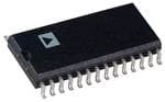
ICGOO电子元器件商城为您提供AD8347ARUZ由Analog设计生产,在icgoo商城现货销售,并且可以通过原厂、代理商等渠道进行代购。 AD8347ARUZ价格参考¥66.00-¥66.00。AnalogAD8347ARUZ封装/规格:RF 解调器, RF Demodulator IC 800MHz ~ 2.7GHz 28-TSSOP (0.173", 4.40mm Width)。您可以下载AD8347ARUZ参考资料、Datasheet数据手册功能说明书,资料中有AD8347ARUZ 详细功能的应用电路图电压和使用方法及教程。
AD8347ARUZ 是由 Analog Devices Inc.(ADI)生产的一款 RF 解调器,广泛应用于无线通信和射频信号处理领域。以下是其主要应用场景:

1. 无线通信系统:
   AD8347ARUZ 可用于无线通信设备中的信号解调,例如蜂窝基站、Wi-Fi 接收器和其他无线数据传输系统。它能够处理高频射频信号,提取基带信息,适用于 2G、3G 和 4G 网络的接收链路。

2. 雷达与导航系统:
   在雷达和导航应用中,AD8347ARUZ 能够对回波信号进行解调,提取目标的距离、速度和角度信息。它适用于脉冲多普勒雷达、连续波雷达以及卫星导航接收机。

3. 测试与测量设备:
   该芯片可用于频谱分析仪、矢量信号分析仪等测试设备中,帮助工程师分析复杂射频信号的特性。其高线性度和低失真性能确保了测量结果的准确性。

4. 软件定义无线电(SDR):
   AD8347ARUZ 支持多种调制方式的解调,适用于 SDR 平台,允许用户通过软件灵活配置接收信号的类型,从而实现多标准通信。

5. 物联网(IoT)设备:
   在 IoT 领域,AD8347ARUZ 可用于低功耗无线传感器网络中的信号解调,支持窄带通信协议,如 LoRa、Sigfox 和 NB-IoT。

6. 卫星通信:
   卫星地面站或便携式卫星终端可以利用 AD8347ARUZ 进行下行链路信号的解调,以接收来自卫星的高清视频、语音或数据流。

7. 医疗设备:
   在医疗领域,该芯片可用于超声成像设备或无线健康监测系统中,解调射频信号以获取生物医学数据。

AD8347ARUZ 的高性能、低噪声和宽动态范围特性使其成为上述应用场景的理想选择,尤其适合需要高精度和可靠性的系统设计。
| 参数 | 数值 |
| 产品目录 | |
| 描述 | IC QUADRATURE DEMOD 28-TSSOP调节器/解调器 800MHz TO 2.7GHz RF/IF Quadrature |
| DevelopmentKit | AD8347-EVALZ |
| 产品分类 | |
| LO频率 | 800MHz ~ 2.7GHz |
| 品牌 | Analog Devices |
| 产品手册 | |
| 产品图片 |
|
| rohs | 符合RoHS无铅 / 符合限制有害物质指令(RoHS)规范要求 |
| 产品系列 | RF集成电路,调节器/解调器,Analog Devices AD8347ARUZ- |
| 数据手册 | |
| P1dB | -30dBm |
| 产品型号 | AD8347ARUZ |
| RF频率 | 800MHz ~ 2.7GHz |
| 产品培训模块 | http://www.digikey.cn/PTM/IndividualPTM.page?site=cn&lang=zhs&ptm=24734 |
| 产品目录页面 | |
| 产品种类 | 调节器/解调器 |
| 供应商器件封装 | 28-TSSOP |
| 功能 | 解调器 |
| 包装 | 管件 |
| 商标 | Analog Devices |
| 噪声系数 | 11dB |
| 增益 | 39.5dB |
| 安装风格 | SMD/SMT |
| 封装 | Tube |
| 封装/外壳 | 28-TSSOP(0.173",4.40mm 宽) |
| 封装/箱体 | TSSOP-28 |
| 工作温度范围 | - 40 C to + 85 C |
| 工作电压 | 2.7 V to 5.5 V |
| 工作电流 | 64 mA |
| 工作电源电压 | 2.7 V to 5.5 V |
| 工厂包装数量 | 50 |
| 接口类型 | LO |
| 最大功率耗散 | 500 mW |
| 最大工作温度 | + 85 C |
| 最小工作温度 | - 40 C |
| 标准包装 | 50 |
| 电压-电源 | 2.7 V ~ 5.5 V |
| 电流-电源 | 80mA |
| 电源电流 | 64 mA |
| 类型 | Demodulator |
| 系列 | AD8347 |
| 视频文件 | http://www.digikey.cn/classic/video.aspx?PlayerID=1364138032001&width=640&height=505&videoID=2245193150001 |
| 调制类型 | Quadrature |


- 商务部:美国ITC正式对集成电路等产品启动337调查
- 曝三星4nm工艺存在良率问题 高通将骁龙8 Gen1或转产台积电
- 太阳诱电将投资9.5亿元在常州建新厂生产MLCC 预计2023年完工
- 英特尔发布欧洲新工厂建设计划 深化IDM 2.0 战略
- 台积电先进制程称霸业界 有大客户加持明年业绩稳了
- 达到5530亿美元!SIA预计今年全球半导体销售额将创下新高
- 英特尔拟将自动驾驶子公司Mobileye上市 估值或超500亿美元
- 三星加码芯片和SET,合并消费电子和移动部门,撤换高东真等 CEO
- 三星电子宣布重大人事变动 还合并消费电子和移动部门
- 海关总署:前11个月进口集成电路产品价值2.52万亿元 增长14.8%


PDF Datasheet 数据手册内容提取
0.8 GHz to 2.7 GHz Direct Conversion Quadrature Demodulator AD8347 FEATURES FUNCTIONAL BLOCK DIAGRAM Integrated RF and baseband AGC amplifiers AD8347 Quadrature phase accuracy 1° typ LOIN 1 28 LOIP I/Q amplitude balance 0.3 dB typ VPS1 2 PHASE 27 COM1 SPLITTER Third-order intercept (IIP3) +11.5 dBm @ min gain IOPN 3 26 QOPN IOPP 4 25 QOPP Noise figure 11 dB @ max gain VCMO 5 PHASE 24 QAIN AGC range 69.5 dB SPLITTER IAIN 6 23 COM3 Baseband level control circuit COM3 7 22 QMXO Low LO drive −8 dBm IMXO 8 21 VPS3 ADC-compatible I/Q outputs COM2 9 20 VDT1 Single supply 2.7 V to 5.5 V RFIN 10 DET 19 VAGC Power-down mode RFIP 11 18 VDT2 28-lead TSSOP package VPS2 12 17 VGIN IOFS 13 16 QOFS APPLICATIONS VREF 14 BIAS COGNATIRNOL 15 ENBL 02675-001 Figure 1. Cellular base stations Radio links Wireless local loop IF broadband demodulators RF instrumentation Satellite modems GENERAL DESCRIPTION The AD83471 is a broadband direct quadrature demodulator Baseband level detectors are included for use in an AGC loop to with RF and baseband automatic gain control (AGC) amplifiers. maintain the output level. The demodulator dc offsets are It is suitable for use in many communications receivers, performing minimized by an internal loop, whose time constant is quadrature demodulation directly to baseband frequencies. The controlled by external capacitor values. The offset control can input frequency range is 800 MHz to 2.7 GHz. The outputs can also be overridden by forcing an external voltage at the offset be connected directly to popular A-to-D converters such as the nulling pins. AD9201 and AD9283. The baseband variable gain amplifier outputs are brought off- The RF input signal goes through two stages of variable gain chip for filtering before final amplification. By inserting a amplifiers prior to two Gilbert-cell mixers. The LO quadrature channel selection filter before each output amplifier, high level phase splitter employs polyphase filters to achieve high out-of-channel interferers are eliminated. Additional internal quadrature accuracy and amplitude balance over the entire circuitry also allows the user to set the dc common-mode level operating frequency range. Separate I and Q channel variable at the baseband outputs. gain amplifiers follow the baseband outputs of the mixers. The RF and baseband amplifiers together provide 69.5 dB of gain control. A precision control circuit sets the linear-in-dB RF gain response to the gain control voltage. 1 U.S. patents issued and pending. Rev. A Information furnished by Analog Devices is believed to be accurate and reliable. However, no responsibility is assumed by Analog Devices for its use, nor for any infringements of patents or other One Technology Way, P.O. Box 9106, Norwood, MA 02062-9106, U.S.A. rights of third parties that may result from its use. Specifications subject to change without notice. No license is granted by implication or otherwise under any patent or patent rights of Analog Devices. Tel: 781.329.4700 www.analog.com Trademarks and registered trademarks are the property of their respective owners. Fax: 781.461.3113 © 2005 Analog Devices, Inc. All rights reserved.
AD8347 TABLE OF CONTENTS Features..............................................................................................1 LO and Phase Splitters...............................................................16 Applications.......................................................................................1 Output Level Detector...............................................................17 Functional Block Diagram..............................................................1 Bias...............................................................................................17 General Description.........................................................................1 Applications.....................................................................................18 Revision History...............................................................................2 Basic Connections......................................................................18 Specifications.....................................................................................3 RF Input and Matching.............................................................18 Absolute Maximum Ratings............................................................5 LO Drive Interface.....................................................................18 ESD Caution..................................................................................5 Operating the VGA....................................................................19 Pin Configuration and Function Descriptions.............................6 Mixer Output Level and Drive Capability..............................19 Typical Performance Characteristics.............................................8 Operating the VGA in AGC Mode..........................................19 RF Amp and Demodulator.........................................................8 Changing the AGC Setpoint.....................................................20 Baseband Output Amplifiers....................................................11 Baseband Amplifiers..................................................................20 RF Amp/Demod and Baseband Output Amplifiers..............12 Driving Capacitive Loads..........................................................21 Equivalent Circuits.....................................................................14 External Baseband Amplification............................................21 Theory of Operation......................................................................16 Filter Design Considerations....................................................21 RF Variable Gain Amplifiers (VGA)........................................16 DC Offset Compensation..........................................................22 Mixers..........................................................................................16 Evaluation Board............................................................................23 Baseband Variable Gain Amplifiers.........................................16 Outline Dimensions.......................................................................26 Output Amplifiers......................................................................16 Ordering Guide..........................................................................26 REVISION HISTORY 10/05—Rev. 0 to Rev. A Updated Format..................................................................Universal Change V to V ..........................................................Universal GIN VGIN Changes to Figure 46......................................................................19 Changes to Figure 48 .....................................................................21 Changes to Figure 49 and Figure 50.............................................22 Changes to Ordering Guide..........................................................27 10/01—Revision 0: Initial Version Rev. A | Page 2 of 28
AD8347 SPECIFICATIONS V = 5 V; T = 25°C; F = 1.9 GHz; V = 1 V; F = 1.905 GHz; P = −8 dBm, R = 10 kΩ, dBm with respect to 50 Ω, unless S A LO VCMO RF LO LOAD otherwise noted. Table 1. Parameter Conditions Min Typ Max Unit OPERATING CONDITIONS LO/RF Frequency Range 0.8 2.7 GHz LO Input Level −10 0 dBm VGIN Input Level 0.2 1.2 V V (V) 2.7 5.5 V SUPPLY S Temperature Range −40 +85 °C RF AMPLIFIER/DEMODULATOR From RFIP/RFIN to IMXO and QMXO (IMXO/QMXO load > 1 kΩ) AGC Gain Range 69.5 dB Conversion Gain (Max) V = 0.2 V (max gain) 39.5 dB VGIN Conversion Gain (Min) V = 1.2 V (min gain) −30 dB VGIN Gain Linearity V = 0.3 V to 1 V ±2 dB VGIN Gain Flatness F = 0.8 GHz to 2.7 GHz, F = 1 MHz +0.7 dB p-p LO BB Input P1 dB V = 0.2 V −30 dBm VGIN V = 1.2 V −2 dBm VGIN Third-Order Input Intercept (IIP3) F = 1.905 GHz, +11.5 dBm RF1 F = 1.906 GHz, –10 dBm each tone, (min gain) RF2 Second-Order Input Intercept (IIP2) F = 1.905 GHz, +25.5 dBm RF1 F = 1.906 GHz, −10 dBm each tone, (min gain) RF2 LO Leakage (RF) At RFIP −60 dBm LO Leakage (MXO) At IMXO/QMXO −42 dBm Demodulation Bandwidth −3 dB +90 MHz Quadrature Phase Error F = 1.9 GHz −3 ±1 +3 degree RF I/Q Amplitude Imbalance F = 1.9 GHz +0.3 dB RF Noise Figure Max Gain 11 dB Mixer AGC Output Level See Figure 34 24 mV p-p Baseband DC Offset At IMXO/QMXO, max gain (corrected, REF to VREF) 2 mV Mixer Output Swing Level at which IMD3 = 45 dBc R = 200 Ω 65 mV p-p LOAD R = 1 kΩ 65 mV p-p LOAD Mixer Output Impedance 3 Ω BASEBAND OUTPUT AMPLIFIER From IAIN to IOPP/IOPN and QAIN to QOPP/QOPN R = 10 kΩ LOAD Gain 30 dB Bandwidth −3 dB (see Figure 22) 65 MHz Output DC Offset (Differential) (V – V ) −200 ±50 +200 mV IOPP IOPN Common-Mode Offset (V + V )/2 − V −40 ±5 +40 mV IOPP IOPN VCMO Group Delay Flatness 0 MHz to 50 MHz +1.8 ns p-p Second-Order Intermod. Distortion F 1 = 5 MHz, F 2 = 6 MHz, V 1 = V 2 = 8 mV p-p −49 dBc IN IN IN IN Third-Order Intermod. Distortion F 1 = 5 MHz, F 2 = 6 MHz, V 1 = V 2 = 8 mV p-p −67 dBc IN IN IN IN Input Bias Current +2 μA Input Impedance 1||3 MΩ||pF Output Swing Limit (Upper) V − 1.3 V S Output Swing Limit (Lower) 0.4 V Rev. A | Page 3 of 28
AD8347 Parameter Conditions Min Typ Max Unit CONTROL INPUT/OUTPUTS VCMO Input @ V = 2.7 V 1 V S @ V = 5 V 0.5 1 2.5 V S Gain Control Input Bias Current VGIN <1 μA Offset Input Overriding Current IOFS, QOFS 10 μA VREF Output R = 10 kΩ 0.95 1.00 1.05 V LOAD RESPONSE FROM RF INPUT TO FINAL IMXO and QMXO connected directly to IAIN and QAIN, BB AMP respectively Gain @ V = 0.2 V 65.5 69.5 72.5 dB VGIN Gain @ V = 1.2 V −3 +0.5 +4 dB VGIN Gain Slope −96.5 −89 −82.5 dB/V Gain Intercept Linear extrapolation back to theoretical value at VGIN = 0 88 94 101 dB LO/RF INPUT (See Figure 30 through Figure 33 for more detail) LOIP Input Return Loss Measuring LOIP LOIN, ac-coupled to ground with 100 pF. −4 dB Measuring through evaluation board balun with termination −9.5 dB RFIP Input Return Loss RFIP input pin −10 dB ENABLE Power-Up Control Low = standby 0 0.5 V Power-Up Control High = enabled +V − 1 +V V S S Power-Up Time Time for final BB amps to be within 90% of final amplitude @ V = 5 V 20 μs S @ V = 2.7 V 10 μs S Power-Down Time Time for supply current to be <4 mA @ V = 5 V 30 μs S @ V = 2.7 V 1.5 ms S POWER SUPPLIES VPS1, VPS2, VPS3 Voltage 2.7 5.5 V Current (Enabled) @ 5 V 48 64 80 mA Current (Standby) @ 5 V 400 μA Current (Standby) @ 3.3 V 80 μA Rev. A | Page 4 of 28
AD8347 ABSOLUTE MAXIMUM RATINGS Table 2. Stresses above those listed under Absolute Maximum Ratings Parameter Rating may cause permanent damage to the device. This is a stress Supply Voltage VPS1, VPS2, VPS3 5.5 V rating only; functional operation of the device at these or any LO and RF Input Power 10 dBm other conditions above those indicated in the operational Internal Power Dissipation 500 mW section of this specification is not implied. Exposure to absolute θ 68°C/W JA maximum rating conditions for extended periods may affect Maximum Junction Temperature 150°C device reliability. Operating Temperature Range −40°C to +85°C Storage Temperature Range −65°C to +150°C Lead Temperature (Soldering 60 sec) 300°C ESD CAUTION ESD (electrostatic discharge) sensitive device. Electrostatic charges as high as 4000 V readily accumulate on the human body and test equipment and can discharge without detection. Although this product features proprietary ESD protection circuitry, permanent damage may occur on devices subjected to high energy electrostatic discharges. Therefore, proper ESD precautions are recommended to avoid performance degradation or loss of functionality. Rev. A | Page 5 of 28
AD8347 PIN CONFIGURATION AND FUNCTION DESCRIPTIONS LOIN 1 28 LOIP VPS1 2 27 COM1 IOPN 3 26 QOPN IOPP 4 25 QOPP VCMO 5 24 QAIN IAIN 6 23 COM3 AD8347 COM3 7 TOPVIEW 22 QMXO IMXO 8 (Not to Scale) 21 VPS3 COM2 9 20 VDT1 RFIN 10 19 VAGC RFIP 11 18 VDT2 VPS2 12 17 VGIN VIOREFSF 1134 1165 EQNOBFLS 02675-002 Figure 2. 28-Lead TSSOP Pin Configuration Table 3. Pin Function Descriptions Equiv. Pin No. Mnemonic Circuit Description 1, 28 LOIN, LOIP A LO Input. For optimum performance, these inputs are differentially driven. Typical input drive level is equal to −8 dBm. To improve the match to a 50 Ω source, connect a 200 Ω shunt resistor between LOIP and LOIN. A single-ended drive is possible, but slightly increases LO leakage. 2 VPS1 Positive Supply for LO Section. Decouple VPS1 with 0.1 μF and 100 pF capacitors. 3, 4 IOPN, IOPP B I-Channel Differential Baseband Output. Typical output swing is equal to 760 mV p-p differential in AGC mode. The common-mode level on these pins is programmed by the voltage on VCMO. 5 VCMO C Baseband Amplifier Common-Mode Voltage. The voltage applied to this pin sets the output common- mode level of the baseband amplifiers. This pin can either be connected to VREF (Pin 14) or to a reference voltage from another device (typically an ADC). 6 IAIN D I-Channel Baseband Amplifier Input. This pin, which has a high input impedance, should be biased to VREF (approximately 1 V). If IAIN is connected directly to IMXO, biasing is provided by IMXO. If an ac- coupled filter is placed between IMXO and IAIN, this pin can be biased from VREF through a 1 kΩ resistor. The gain from IAIN to the differential outputs IOPN/IOPP is 30 dB. 7, 23 COM3 Ground for Biasing and Baseband Sections. 8, 22 IMXO, QMXO B I-Channel and Q-Channel Baseband Mixer/VGA Outputs. Low impedance outputs with bias levels equal to VREF. IMXO and QMXO are typically connected to IAIN and QAIN, respectively, either directly or through filters. These outputs have a maximum current limit of about 1.5 mA. This allows for a 600 mV p-p swing into a 200 Ω load. This corresponds to an input level of −40 dBm @ a maximum gain of 39.5 dB. At lower output levels, IMXO and QMXO can drive a lower load resistance, subject to the same current limit. 9 COM2 RF Section Ground. 10, 11 RFIN, RFIP E RF Input. RFIN must be ac-coupled to ground. The RF input signal should be ac-coupled into RFIP. For a broadband 50 Ω input impedance, connect a 200 Ω resistor from the signal side of the RFIP coupling capacitor to ground. Note that RFIN and RFIP are not interchangeable differential inputs. RFIN is the ground reference for the input system. 12 VPS2 Positive Supply for RF Section. Decouple VPS2 with 0.1 μF and 100 pF capacitors. 13, 16 IOFS, QOFS F I-Channel and Q-Channel Offset Nulling Inputs. To null the dc offset on the I-channel and Q-channel mixer outputs (IMXO, QMXO), connect a 0.1 μF capacitor from these pins to ground. Alternately, a forced voltage of approximately 1 V on these pins disables the offset compensation circuit. 14 VREF G Reference Voltage Output. This output voltage (1 V) is the main bias level for the device and can be used to externally bias the inputs and outputs of the baseband amplifiers. The VREF pin should be decoupled with a 0.1 μF capacitor to ground. 15 ENBL H Chip Enable Input. Active high. 17 VGIN C Gain Control Input. The voltage on this pin controls the gain on the RF and baseband VGAs. The gain control is applied in parallel to all VGAs. The gain control voltage range is from 0.2 V to 1.2 V and corresponds to a gain range from +39.5 dB to −30 dB. This is the gain to the output of the baseband VGAs (that is, QMXO and IMXO). There is an additional 30 dB of gain in the baseband amplifiers. Note that the gain control function has a negative sense (that is, increasing control voltage decreases gain). In AGC mode, connect this pin directly to VAGC. Rev. A | Page 6 of 28
AD8347 Equiv. Pin No. Mnemonic Circuit Description 18, 20 VDT2, VDT1 D Detector Inputs. These pins are the inputs to the on-board detector. VDT2 and VDT1, which have high input impedances, are normally connected to IMXO and QMXO, respectively. 19 VAGC I AGC Output. This pin provides the output voltage from the on-board detector. In AGC mode, connect this pin directly to VGIN. 21 VPS3 Positive Supply for Biasing and Baseband Sections. Decouple VPS3 with 0.1 μF and 100 pF capacitors. 24 QAIN D Q-Channel Baseband Amplifier Input. Bias this high input impedance pin to VREF (approximately 1 V). If QAIN is directly connected to QMXO, biasing is provided by QMXO. If an ac-coupled filter is placed between QMXO and QAIN, this pin can be biased from VREF through a 1 kΩ resistor. The gain from QAIN to the QOPN/QOPP differential outputs is 30 dB. 25, 26 QOPP, QOPN B Q-Channel Differential Baseband Output. Typical output swing is equal to 760 mV p-p differential. The common-mode level on these pins is programmed by the voltage on VCMO. 27 COM1 LO Section Ground. VPS1 VPS2 VPS3 VREF IMXO IOFS IAIN IOPP IOPN 2 12 21 14 8 13 6 4 3 AD8347 VREF BIAS ENBL 15 CELL VREF 5 VCMO VCMO RFIN 10 1 LOIN PHASE PHASE RFIP 11 SPLITTER SPLITTER 2 1 28 LOIP VCMO 7 COM3 9 COM2 GAIN VGIN 17 CONTROL DET 1 DET 2 23 COM3 INTERFACE VREF 27 COM1 VD20T1 VA1G9C VD18T2 QM22XOQO16FS QA24IN QO25PP QO26PN 02675-003 Figure 3. Block Diagram Rev. A | Page 7 of 28
AD8347 TYPICAL PERFORMANCE CHARACTERISTICS RF AMP AND DEMODULATOR 45 14 3.0 40 TA =–40°C 12 35 TA = +85°C 10 2.5 30 8 25 2.0 20 TA = +25°C 6 dB) VS = 2.7V, TA = +25°C R GAIN (dB) 110505 024 TY ERROR ( AIN (dB)11..05 VS = 2.7V, TA =–40°C VS = 5V, TA = +25°C MIXE–1–05 TA = +25°C TA =–40°C ––42NEARI G0.5 VS = 5V, TA =–40°C –15 –6LI 0 VS = 5V, TA = +85°C –20 TA = +85°C –8 –25 –0.5 –30 –10 VS = 2.7V, TA = +85°C –350.2 0.3 0.4 0.5 0.6VVG0I.N7(V)0.8 0.9 1.0 1.1 1.2–12 02675-013 –1.0800 1000 1200 14R00F F1R6E0Q0UE1N80C0Y (2M0H0z0) 2200 2400 2600 02675-016 Figure 4. Gain and Linearity Error vs. VVGIN, Figure 7. Gain vs. FLO, VVGIN = 0.7 V, FBB = 1 MHz VS = 5 V, FLO = 1900 MHz, FBB = 1 MHz 45 14 –27 4305 TA =–40°C 1102 –28 VS = 5V, TA = +25°C VS = 2.7V, TA =–40°C MIXER GAIN (dB)––12311–120000555505 TTAA = = +–8450°°CCTA = +25°CTA = +25°C ––0246842 LINEARITY ERROR (dB) GAIN (dB)––––––332333409321 VSV S= =5 V2,. 7TVA, =T A+ 8=5 +°VC25S °=C 5V, TA =V–S4 =0° 2C.7V, TA = +85°C –20 –35 –6 –25 TA = +85°C –8 –36 –30 –350.2 0.3 0.4 0.5 0.6VV0G.I7N(V)0.8 0.9 1.0 1.1 1.2–10 02675-014 –37800 1000 1200 140R0F F1R6E0Q0UE18N0C0Y (2M0H00z) 2200 2400 2600 02675-017 Figure 5. Gain and Linearity Error vs. VVGIN, Figure 8. Gain vs. FLO, VVGIN = 1.2 V, FBB = 1 MHz VS = 2.7 V, FLO = 1900 MHz, FBB = 1 MHz 40 42 39 41 VS = 2.7V, TA = +25°C VS = 2.7V, TA =–40°C 40 38 VS = 2.7V, TA = +25°C VS = 5V, TA = +25°C 39 37 VS = 5V, TA =–40°C 38 VS = 2.7V, TA =–40°C VS = 5V, TA = +25°C B) 36 B) 37 GAIN (d 3345 VS = 2.7V, TA = +85°C GAIN (d 3365 VS = 2.7V, TA = +85°C VS = 5V, TA =–40°C VS = 5V, TA = +85°C 34 33 33 VS = 5V, TA = +85°C 32 32 31 31 30800 1000 1200 140R0F F1R6E0Q0UE18N0C0Y (2M0H00z) 2200 2400 2600 02675-015 301 BASEBAND FR1E0QUENCY (MHz) 10002675-018 Figure 6. Gain vs. FLO, VVGIN = 0.2 V, FBB = 1 MHz Figure 9. Gain vs. FBB, VVGIN = 0.2 V, FLO = 1900 MHz Rev. A | Page 8 of 28
AD8347 10 15 9 14 VS = 2.7V, TA = V+8S5 =° C5V, TA = +85°C 8 VS = 5V, TA = +25°C 7 13 6 VS = 2.7V, TA = +85°C 12 5 VS = 5V, TA = +85°C B) 4 VS = 2.7V, TA = +25°C m) 11 VS = 2.7V, TA =–40°C GAIN (d 123 IIP3 (dB 109 VS = 2.7VV, ST =A 5=V +,2 T5A°C =–40°C 0 VS = 5V, TA = +25°C 8 –1 –2 VS = 2.7V, TA =–40°C 7 –3 VS = 5V, TA =–40°C 6 –4 –51 BASEBAND FR1E0QUENCY (MHz) 10002675-019 5800 1000 1200 14R00F F1R6E0Q0UE1N80C0Y (M20H0z0) 2200 2400 2600 02675-022 Figure 10. Gain vs. FBB, VVGIN = 0.7 V, FLO = 1900 MHz Figure 13. IIP3 vs. FLO, VVGIN = 1.2 V, FBB = 1 MHz –25 –10 VS = 2.7V, TA = +85°C –26 VS = 2.7V, TA =–40°C –12 VS = 5V, TA = +25°C VS = 2.7V, TA = +25°C –27 VS = 2.7V, TA = +25°C –14 –28 –16 VS = 5V, TA = +25°C –29 –18 B) m) GAIN (d––3301 VS = 5V, TA =–40°C IIP3 (dB––2220 –32 –24 VS = 2.7V, TA =–40°C –33 VS = 2.7V, TA = +85°C VS = 5V, TA = +85°C –26 VS = 5V, TA =–40°C VS = 5V, TA = +85°C –34 –28 –351 BASEBAND FR1E0QUENCY (MHz) 10002675-020 –30800 1000 1200 14R00F F1R6E0Q0UE1N80C0Y (M20H0z0) 2200 2400 2600 02675-023 Figure 11. Gain vs. FBB, VVGIN = 1.2 V, FLO = 1900 MHz Figure 14. IIP3 vs. FLO, VVGIN = 0.2 V, FBB = 1 MHz 0 15 VS = 5V, TA =–40°C –5 VS = 2.7V, TA =–40°C VS = 2.7V, TA = +85°C 14 m)–10 VS = 5V, TA = +85°C VS = 5V, TA = +85°C VS = 2.7V, TA = +85°C dB–15 m) 13 UT P1dB (–20 IIP3 (dB 12 VS = 5V, TA =–40°C P N I–25 VS = 2.7V, TA = +25°C 11 VS = 5V, TA = +25°C –30 VS = 2.7V, TA =–40°C VS = 2.7V, TA = +25°C VS = 5V, TA = +25°C –350.2 0.3 0.4 0.5 0.6VVG0I.N7 (V)0.8 0.9 1.0 1.1 1.2 02675-021 100 5 1015202B5A3S0E3B5A4N0D 4F5R5E0Q5U5EN60CY65 (M7H0z7)58085909510002675-024 Figure 12. Input 1 dB Compression Point (OP1 dB) vs. VVGIN, Figure 15. IIP3 vs. FBB, VVGIN = 1.2 V, FLO = 1900 MHz FLO = 1900 MHz, FBB = 1 MHz Rev. A | Page 9 of 28
AD8347 –10 70 15 –12 10 –14 60 VS = 5V, TA = +85°C 5 –16 50 –18 VS = 2.7V, TA = +85°C B) 0 d IIP3 (dBm) –––222420 VS = 5VV, ST A= =5 V+,2 T5°AC =–40°C SE FIGURE ( 4300 VS = 5V ––150IIP3 –26 VS = 2.7V, TA = +25°C NOI 20 VS = 2.7V –15 –28 –20 –30 10 ––33420VTA5S ==1 2–0.4710V5°,C202B5A3S0E3B5A4N0D 4F5R5E0Q5U5EN60CY6 5(M7H0z7)58085909510002675-025 00.2 VS0 =.3 5V 0.V4S = 2.07.V5 VVG0.IN6 (V) 0.7 0.8 0.9 1.0––3205 02675-028 Figure 16. IIP3 vs. FBB, VVGIN = 0.2 V, FLO = 1900 MHz Figure 19. Noise Figure and IIP3 vs. VVGIN, Temperature = 25°C, FLO = 1900 MHz, FBB = 1 MHz 50 2.5 2.0 s) 45 gree 1.5 e D 40 R ( 1.0 O m) ERR 0.5 LO FREQUENCY = 2700MHz IIP2 (dB 35 E PHASE –0.50 30 R U–1.0 T 25 UADRA–1.5 LO FREQUENCY = 800MLHOz FREQUENCY = 1900MHz Q–2.0 20800 1000 1200 14R00F F1R6E0Q0UE1N80C0Y (2M0H0z0) 2200 2400 2600 02675-026 –2.5–20 –18 –16 –1L4O IN–1P2UT L–E10VEL –(d8Bm)–6 –4 –2 002675-029 Figure 17. IIP2 vs. FLO, VVGIN = 1.2 V, Baseband Tone1 = 5 MHz, −10 dBm, Figure 20. Quadrature Error vs. LO Power Level, Temperature = 25°C, Baseband Tone2 = 6 MHz, −10 dBm, Temperature = 25°C, VS = 5 V VVGIN = 0.2 V, VS = 5 V 13.0 14.0 13.5 12.5 13.0 12.5 2700MHz B) 12.0 B) E (d E (d12.0 R R GU 11.5 GU11.5 FI FI E E 11.0 1900MHz S S OI 11.0 OI N N10.5 VS = 5V VS = 2.7V 10.0 800MHz 10.5 9.5 10.0800 1000 1200 14L0O0 F1R6E0Q0UE1N80C0Y (2M0H0z0) 2200 2400 2600 02675-027 9.0–20 –18 –16 –1L4O IN–1P2UT L–E10VEL –(d8Bm)–6 –4 –2 0 02675-030 Figure 18. Noise Figure vs. LO Frequency (FLO), Temperature = 25°C, Figure 21. Noise Figure vs. LO Input Level, Temperature = 25°C, VVGIN = 0.2 V, FBB = 1 MHz VVGIN = 0.2 V, VS = 5 V Rev. A | Page 10 of 28
AD8347 BASEBAND OUTPUT AMPLIFIERS 34 20 32 TA =–40°C, VS = 5V TA =–40°C, VS = 2.7V ms) 15 TA =–40°C, VS = 5V V r TA = +25°C, VS = 5V 30 dB 10 dB) 2268 TA = +85°CT,A V =S +=2 25.°7CV, VS = 5V UTPUT IP3 ( 05 TA =T +A8 5=° +C2, 5V°SC =, V 2TS.7A =V =2.–74V0°C, VS = 2.7V TA = +85°C, VS = 5V GAIN ( 24 TA = +25°C, VS = 2.7V FIER O–1–05 22 TA = +85°C, VS = 5V MPLI–15 A 20 D N–20 A B 18 E–25 S A 161 BASEBAND FR1E0QUENCY (MHz) 10002675-031 B–301 BASEBAND FR1E0QUENCY (MHz) 10002675-033 Figure 22. Gain vs. FBB, VVCMO = 1 V Figure 24. OIP3 vs. FBB, VVCMO = 1 V 5 8 TA =–40°C, VS = 5V TA = +85°C, VS = 5V VS = 2.7V, MEAN +σ 0 6 VS = 2.7V, MEAN TA = +25°C, VS = 5V mV) BV rms)–1–05 TA = +2T5A° C=,– V4S0 °=C 2, .V7SV = 2.7V E OFFSET ( 42 VS = 5V, MEAN VS = 5V, MEAN +σ d D OP1 ( TA = +85°C, VS = 2.7V N-MO 0 –15 O M–2 M –20 CO VS = 2.7V, MEAN–σ –4 VS = 5V, MEAN–σ –251 BASEBAND FR1E0QUENCY (MHz) 10002675-032 –60.5 1.0 1.5 VVC2M.O0 (V) 2.5 3.0 3.502675-034 Figure 23. OP1 vs. FBB, VVCMO = 1 V Figure 25. Common-Mode Output Offset Voltage vs. VVCMO, Temperature = 25°C (σ = 1 Standard Deviation) Rev. A | Page 11 of 28
AD8347 RF AMP/DEMOD AND BASEBAND OUTPUT AMPLIFIERS 75 1.0 65 TTTAAA === +––442005°°°CCC,,, VVVSSS === 252.V.77VV dB) 00..68 55 TA = +25°C, VS = 5V H ( AIN(dB)45 TVAS == +2.875V°C, MISMATC 00..24 TA = +85°C GE G35 TA = +85°C, VS = 5V UDE 0 TA = +25°C OLTA25 MPLIT–0.2 V A–0.4 15 O Q –0.6 TA =–40°C T 5 I –0.8 –50.2 0.3 0.4 0.5 0.6VVG0.IN7(V)0.8 0.9 1.0 1.1 1.2 02675-035 –1.00 5 1B0ASEB1A5ND FR2E0QUENC25Y (MHz3)0 35 4002675-038 Figure 26. Voltage Gain vs. VVGIN, FLO = 1900 MHz, FBB = 1 MHz Figure 29. I/Q Amplitude Imbalance vs. FBB, Temperature = 25°C, VS = 5 V 2.5 0 s) 2.0 ee –2 gr 1.5 e D R ( 1.0 m) –4 O B HASE ERR 0.50 TA = +25°C, VS = 5V N LOSS (d –6 RF WITH TERMINATION P–0.5 R URE –1.0 RETU –8 AT UADR–1.5 TA = +85°C, VS = 5V TA =–40°C, VS = 5V –10 Q–2.0 RF WITHOUT TERMINATION –2.5800 1000 1200 14R00F F1R6E0Q0UE1N80C0Y (2M0H0z0) 2200 2400 2600 02675-036 –12800 1000 1200 140R0F F1R6E0Q0UE18N0C0Y (2M0H00z) 2200 2400 2600 02675-039 Figure 27. Quadrature Phase Error vs. FLO, VVGIN = 0.7 V, VS = 5 V Figure 30. Return Loss of RFIP vs. FRF, VVGIN = 0.7 V, VS = 5 V 2.5 s) 2.0 e e gr 1.5 e D R ( 1.0 O RR 0.5 2.7GHz WITH TERMINATION E ASE 0 TA = +85°C H 800MHz P–0.5 RE TA = +25°C ATU–1.0 TA =–40°C DR–1.5 2.7GHz 800MHz UA WITHOUT TERMINATION Q–2.0 –2.50 5 1B0ASEB1A5ND FR2E0QUENC25Y (MHz3)0 35 40 02675-037 02675-040 Figure 28. Quadrature Phase Error vs. FBB, VVGIN = 0.7 V, VS = 5 V Figure 31. S11 of RFIN vs. FRF, VVGIN = 0.7 V, VS = 5 V Rev. A | Page 12 of 28
AD8347 0 30 1.20 TA =–40°C –2 p)25 TA = +85°C 1.00 p- LO PORT WITHOUT TERMINATION V –4 m RETURN LOSS (dBm)–1––806 R OUTPUT VOLTAGE (211005 TA = +25°C TA = +85°C TA =TA– 4=0 +°C25°C 000...864000 AGC VOLTAGE (V) E X MI 5 0.20 –12 LO PORT WITH TERMINATION –14800 1000 1200 140R0F F1R6E0Q0UE18N0C0Y (2M0H00z) 2200 2400 2600 02675-041 0–70 –60 –50 RF –IN40PUT P–O30WER –(d2B0m) –10 0 100 02675-043 Figure 32. Return Loss of LOIP vs. FLO, VVGIN = 0.7 V, VP = 5 V Figure 34. AGC Voltage and Mixer Output Level vs. RF Input Power, FLO = 1900 MHz, FBB = 1 MHz, VS = 5 V 85 80 WITH TERMINATION 800MHz A) 75 T (m 70 VP = 5V N RE VP = 5.5V R 65 2.7GHz U 2.7GHz C Y L 60 P UP VP = 3V S 55 800MHz VP = 2.7V 50 WITHOUT TERMINATION 02675-042 45–40 –30 –20 –10 0TEM10PER2A0TU3R0E (°4C0) 50 60 70 80 02675-044 Figure 33. S11 of LOIN vs. FLO, VVGIN = 0.7 V, VS = 5 V Figure 35. Supply Current vs. Temperature, VVGIN = 0.7 V, VVCMO = 1 V Rev. A | Page 13 of 28
AD8347 EQUIVALENT CIRCUITS VPS1 VPS3 LOIN IAIN QAIN PHASE SPLITTER CONTINUES LOIP COM1 02675-004 COM3 02675-007 Figure 36. Circuit A Figure 39. Circuit D VPS3 VPS2 IOPP,IOPN, QOPP,QOPN, IMXO,QMXO RFIP RFIN COM3 02675-005 COM2 02675-008 Figure 37. Circuit B Figure 40. Circuit E VPS3 VPS3 IOFS VCMO QOFS CURRENT MIRROR CURRENT MIRROR COM3 02675-006 COM3 02675-009 Figure 38. Circuit C Figure 41. Circuit F Rev. A | Page 14 of 28
AD8347 VPS3 VPS3 VREF VAGC COM3 02675-010 COM3 02675-012 Figure 42. Circuit G Figure 44. Circuit I VPS3 ENBL COM3 02675-011 Figure 43. Circuit H Rev. A | Page 15 of 28
AD8347 THEORY OF OPERATION VPS1 VPS2 VPS3 VREF IMXO IOFS IAIN IOPP IOPN 2 12 21 14 8 13 6 4 3 AD8347 VREF BIAS ENBL 15 CELL 5 VCMO VREF VCMO RFIN 10 1 LOIN PHASE PHASE RFIP 11 SPLITTER SPLITTER 2 1 28 LOIP 7 COM3 VCMO 9 COM2 GAIN VGIN 17 CONTROL DET 1 DET 2 23 COM3 INTERFACE VREF 27 COM1 VD20T1 VA1G9C VD18T2 QM22XOQO16FS Q2A4IN QO25PP QO26PN 02675-045 Figure 45. Block Diagram The AD8347 is a direct I/Q demodulator usable in digital differential currents are split and fed to the two Gilbert-cell wireless communication systems including cellular, PCS, and mixers through separate cascode stages. digital video receivers. An RF signal in the frequency range of MIXERS 800 MHz to 2,700 MHz is directly downconverted to the I and Q components at baseband using a local oscillator (LO) signal Two double balanced Gilbert-cell mixers, one for each channel, at the same frequency as the RF signal. perform the in-phase (I) and quadrature (Q) down conversion. Each mixer has four cross-connected transistor pairs that are The RF input signal goes through two stages of variable gain terminated in resistive loads and feed the differential baseband amplifiers before splitting up to reach two Gilbert-cell mixers. variable gain amplifiers for each channel. The quadrature LO The mixers are driven by a pair of LO signals which are in signals drive the bases of the mixer transistors. quadrature (90 degrees of phase difference). The outputs of the mixers are applied to baseband I-channel and Q-channel BASEBAND VARIABLE GAIN AMPLIFIERS variable gain amplifiers. The outputs from these baseband The baseband VGAs also use the X-AMP approach with NPN variable gain amplifiers are brought out to pins for external differential pairs separated by sections of resistive attenuators. filtering. The filter outputs are then applied to a pair of on-chip, The same interpolator controlling the RF amplifiers controls the fixed gain, baseband amplifiers. These amplifiers gain up the tail currents of the differential pairs. The outputs of these amplifiers outputs from the external filters to a level compatible with most are provided off chip for external filtering. Automatic offset A-to-D converters. A sum of squares detector is available for nulling minimizes the dc offsets at both I- and Q-channels. The use in an automatic gain control (AGC) loop to set the output common-mode output voltage is set to the same level as the level. The RF and baseband amplifiers provide approximately reference voltage (1.0 V) generated in the Bias cell, also made 69.5 dB of gain control range. Additional on-chip circuits allow available at the VREF pin (see Figure 45). the setting of the dc level at the I-channel and Q-channel baseband outputs, as well as nulling the dc offset at each OUTPUT AMPLIFIERS channel. The output amplifiers gain up the signal coming back from each of the external filters to a level compatible with most high speed A-to- RF VARIABLE GAIN AMPLIFIERS (VGA) D converters. These amplifiers are based on an active feedback These amplifiers use the patented X-AMP® approach with NPN design to achieve high gain bandwidth with low distortion. differential pairs separated by sections of resistive attenuators. The gain control is achieved through a gaussian interpolator LO AND PHASE SPLITTERS where the control voltage sets the tail currents supplied to the The incoming LO signal is applied to a polyphase phase splitter various differential pairs according to the gain desired. In the to generate the LO signals for the I-channel and Q-channel first amplifier, the combined output currents from the mixers. The polyphase phase splitters are RC networks transconductance cells go through a cascode stage to resistive connected in a cyclical manner to achieve gain balance and loads with inductive peaking. In the second amplifier, the phase quadrature. The wide operating frequency range of these phase splitters is achieved by cascading multiple sections of Rev. A | Page 16 of 28
AD8347 these networks with staggered RC constants. Each branch goes BIAS through a buffer to make up for the loss and high frequency An accurate reference circuit generates the reference currents roll-off. The output from the buffers then goes into another used by the different sections. The reference circuit is controlled polyphase phase splitter to enhance the accuracy of phase by an external power-up (ENBL) logic signal that, when set low, quadrature. Each LO signal is buffered again to drive the puts the whole chip into a sleep mode typically requiring less mixers. than 400 μA of supply current. The reference voltage (VREF) of OUTPUT LEVEL DETECTOR 1.0 V, that serves as the common-mode reference for the baseband circuits, is made available for external use. The VREF To create an AGC voltage (VAGC), two signals proportional to pin should be decoupled with a 0.1 μF capacitor to ground. the square of each output channel are summed together and compared to a built-in threshold. The inputs to this rms detector are referenced to VREF. Rev. A | Page 17 of 28
AD8347 APPLICATIONS BASIC CONNECTIONS RF INPUT AND MATCHING The basic connections for operating the AD8347 are shown in The RF input signal should be ac-coupled into the RFIP pin and Figure 46. The device is powered through three power supply RFIN should be ac-coupled to ground. To improve broadband pins: VPS1, VPS2, and VPS3. These pins supply current to matching to a 50 Ω source, a 200 Ω resistor can be connected different parts of the overall circuit. VPS1 and VPS2 power the from the signal side of the RFIP coupling capacitor to ground. local oscillator (LO) and RF sections, respectively, while VPS3 LO DRIVE INTERFACE powers the baseband amplifiers. Connect all of these pins to the same supply voltage; however, separately decouple each pin For optimum performance, the LO inputs, LOIN and LOIP, using two capacitors. 100 pF and 0.1 μF capacitors are should be driven differentially; the M/A-COM balun, ETC1-1-13 recommended, though values close to these can be used. is recommended. Unless an ac-coupled transformer is used to generate the differential LO, the inputs must be ac-coupled, as Use a supply voltage in the range 2.7 V to 5.5 V. The quiescent shown in Figure 46. To improve broadband matching to a 50 Ω current is 64 mA when operating from a 5 V supply. By pulling source, connect a 200 Ω shunt resistor between LOIP and LOIN. the ENBL pin low, the device goes into its power-down mode. The power-down current is 400 μA when operating on a 5 V A LO drive level of −8 dBm is recommended. Figure 20 shows supply and 80 μA on a 2.7 V supply. the relationship between LO drive level, LO frequency, and quadrature error for a typical device. Like the supply pins, the individual sections of the circuit are separately grounded. COM1, COM2, and COM3 provide A single-ended drive is also possible as shown in Figure 47, but ground for the LO, RF, and baseband sections, respectively. this slightly increases LO leakage. Apply the LO signal through Connect all of these pins to the same low impedance ground. a coupling capacitor to LOIP, and ac-couple LOIN to ground. Because the inputs are fully differential, the drive orientation can be reversed. As in the case of the differential drive, a 200 Ω resistor connected across LOIP and LOIN improves the match to a 50 Ω source. +VS (2.7V–5.5V) IOPP C6 C5 C7 C8 C9 C10 24mV p-p 0.1μF 100pF 0.1μF100pF0.1μF100pF (AGC MODE) C16 1V BIAS (VREF) 0.1μF 760mV p-p C13 DIFFERENTIAL 0.1μF (AGC MODE) VCM = 1V VPS1 VPS2 VPS3 VREF IMXO IOFS IAIN IOPP IOPN 2 12 21 14 8 13 6 4 3 AD8347 VREF IOPN VREF BIAS ENBL15 CELL VCMO LO INPUT 10C01pF VCMO 5 10C04pF 0.8G–H8zd–B2m.7GHz RFIN R1 10 1 LOIN 3 4 200Ω RFIP PHASE PHASE R17 11 SPLITTER SPLITTER LOIP 200Ω C2 2 1 28 1 5 0.80RGdFHB zmIN– 2PM.U7AGTXHz 100pF VCMO 7 COM3 10C03pF E(MT/CA T-1C1-1O-M13) (AGC MODE) 9 COM2 VGIN GAIN COM3 17 CONTROL DET 1 DET 2 23 INTERFACE VREF COM1 27 QOPN 20 19 18 22 16 24 25 26 VDT1 VAGC VDT2 QMXO QOFS QAIN QOPP QOPN C14 0.1μF 760mV p-p C15 DIFFERENTIAL 0.1μF 24mV p-p (AGC MODE) (AGC MODE) VCM = 1V 1V BIAS (VREF) QOPP 02675-046 Figure 46. Basic Connections Rev. A | Page 18 of 28
AD8347 These output stages are not, however, designed to directly drive 100pF LO LOIN 50 Ω loads. 200Ω AD8347 OPERATING THE VGA IN AGC MODE LOIP 100pF 02675-047 Aa DlthAoCu,g thh eth Ae DV8G3A47 c hanas b aen d orniv-ebno abryd a snu mex toefr nsqaul saoreusr cdee tseucctho ra tso Figure 47. Single-Ended LO Drive allow the AD8347 to operate in an automatic leveling mode. Due to the nature of the detector, an input signal with a higher OPERATING THE VGA peak-to-average ratio causes the AGC loop to settle with a A three-stage VGA sets the gain in the RF section. Two of the higher mixer output peak-to-peak voltage. In this data sheet, three stages come before the mixer while the third amplifies the peak-to-peak calculations assume a sine wave input when mixer output. All three stages are driven in parallel. The gain referencing AGC operation. range of the first RF VGA and that of the second RF VGA The connections for operating in this mode are shown in combined with the mixer are both −13 dB to +10 dB. The gain Figure 46. The two mixer outputs are connected to Detector range of the baseband VGA is −4 dB to +19.5 dB. Therefore, the Input VDT1 and Detector Input VDT2. The summed detector overall gain range from the RF input to the IMXO and QMXO output drives an internal integrator which, in turn, delivers a pins is −30 dB to approximately +39.5 dB. gain correction voltage to the VAGC pin. A 0.1 μF capacitor The gain of the VGA is set by the voltage on the VGIN pin, from VAGC to ground sets the dominant pole of the integrator which is a high impedance input. The gain control function circuit. VAGC, which should be connected to VGIN, adjusts (which is linear-in-dB) and linearity are shown in Figure 4 and gain until an internal threshold is reached. This threshold Figure 5 at 1.9 GHz. Note that the sense of the gain control corresponds to a level at the IMXO and QMXO pins of approxi- voltage is negative because as the gain control voltage ranges mately 8.5 mV rms. This level changes slightly as a function of from 0.2 V to 1.2 V, the gain decreases from +39.5 dB to −30 dB. RF input power (see Figure 34). For a CW (sine wave) input, this corresponds to approximately 24 mV p-p. If this signal is MIXER OUTPUT LEVEL AND DRIVE CAPABILITY applied directly to the subsequent baseband amplifier stage, I- and Q-channel baseband outputs, IMXO and QMXO, are the final baseband output is 760 mV p-p differential. See the low impedance outputs (R @ 3 Ω) with bias levels equal to Baseband Amplifiers section. OUT V , the voltage on Pin 14. The achievable output levels on VREF If the VGA gain is set from an external source, VDT1 and IMXO/QMXO are limited by their current drive capability of VDT2 (the on-board detector inputs) are not used and are tied 1.5 mA maximum. This allows for a 600 mV p-p swing into a to VREF. 200 Ω load. At lower output levels, IMXO and QMXO can drive smaller load resistances, subject to the same current limit. Rev. A | Page 19 of 28
AD8347 R19 1kΩ +VS +5V R20 4kΩ 2.5V IOPP C6 C5 C7 C8 C9 C10 0.1μF 100pF 0.1μF100pF0.1μF100pF 120mV p-p C16 1V BIAS 0.1μF 3.8V p-p C13 DIFFERENTIAL 0.1μF VCM = 2.5V VPS1 VPS2 VPS3 VREF IMXO IOFS IAIN IOPP IOPN 2 12 21 14 8 13 6 4 3 AD8347 VREF IOPN VREF BIAS ENBL15 CELL VCMO LO INPUT 10C01pF VCMO 5 10C04pF 0.8G–H8zd–B2m.7GHz RFIN R1 10 1 LOIN 3 4 200Ω RFIP PHASE PHASE R17 11 SPLITTER SPLITTER LOIP 200Ω C2 2 1 28 1 5 100pF T1 RF COM3 C3 ETC 1-1-13 INPUT VCMO 7 100pF (M/A-COM) COM2 VGIN 9 GAIN COM3 17 CONTROL DET 1 DET 2 23 INTERFACE VREF COM1 27 QOPN 20 19 18 22 16 24 25 26 VDT1 VAGC VDT2 QMXO QOFS QAIN QOPP QOPN C14 0.1μF 3.8V p-p DIFFERENTIAL R21 1210Vm BVIA pS-p VCM = 2.5V 4kΩ 1Rk2Ω2 QOPP 02675-048 Figure 48. Adjusting AGC Level to Increase Baseband Amplifier Output Swing CHANGING THE AGC SETPOINT IOPP, QOPN, and QOPP) deliver a differential voltage of approximately 760 mV p-p (380 mV p-p on each side). The AGC circuit can be easily set up to level at voltages higher than the nominal 24 mV p-p, as shown in Figure 48. The The single-ended input signal to the baseband amplifiers is voltages on Pin IMXO and Pin QMXO are attenuated before applied at IAIN and QAIN, the high impedance inputs. As being applied to the detector inputs. In the example shown, an shown in Figure 46, the baseband amplifier operates internally attenuation factor of 0.2 (−14 dB) between IMXO and QMXO as a differential amplifier, with the second input driven by V . VREF and the detector inputs causes the VGA to level at approximately Therefore, bias the input signal to the baseband amplifier at V . VREF 120 mV p-p (note that the resistor divider network must be The output common-mode level of the baseband amplifiers is referenced to V ). This results in a peak-to-peak output VREF set by the voltage on Pin 5, VCMO. Connect this pin to VREF swing at the baseband amplifier outputs of 3.8 V differential, (Pin 14) or to an external reference voltage from a device such that is, 1.6 V to 3.4 V on each side. Note that V has been VCMO as an analog-to-digital converter (ADC). V has a nominal increased to 2.5 V to avoid signal clipping at the baseband VCMO range from 0.5 V to 2.5 V. However, since the baseband amplifiers outputs. Due to the attenuation between the mixer output and can only swing down to 0.4 V, higher values of V are gener- the detector input, the variation in the settled mixer output level VCMO ally required to avoid low end signal clipping. Alternatively, the vs. RF input power will be greater than the variation shown in positive swing at each output is limited to 1.3 V below the Figure 34. The variation will be greater by a factor equal to the supply voltage; therefore, the maximum p-p swing is given by inverse of the attenuation factor. 2 × (V − 1.3 − 0.4) V differentially. PS BASEBAND AMPLIFIERS For example, for the baseband output amplifier to deliver an The final baseband amplifier stage takes the signals from IMXO output swing of 2 V p-p (1 V p-p on each side), V must be VCMO and QMXO and amplifies them by 30 dB, or a factor of 31.6. in a range from 0.9 V to 2.5 V. This results in a maximum system gain of 69.5 dB. When the VGA is in AGC mode, the baseband I and Q outputs (IOPN, Rev. A | Page 20 of 28
AD8347 The differential output offset voltages of the baseband amplifiers FILTER DESIGN CONSIDERATIONS are typically ±50 mV. This offset voltage results from both input Baseband low-pass or band-pass filtering can be conveniently and output effects. performed between the mixer outputs (IMXO and QMXO) and the input to the baseband amplifiers. Because the output impedance of The overall signal-to-noise ratio can be improved by increasing the mixer is low (approximately 3 Ω) and the input impedance of the VGA gain by driving it with an external voltage or by changing the baseband amplifier is high, it is not practical to design a the setpoint of the AGC circuit. See the Changing the AGC filter that is reactively matched to these impedances. An LC Setpoint section. filter can be matched by placing a series resistor at the mixer DRIVING CAPACITIVE LOADS output and a shunt resistor (terminated to V ) at the input to VREF In applications where the baseband amplifiers are driving the baseband amplifier. unbalanced capacitive loads, place some series resistance between Because the mixer output drive level is limited to a maximum the amplifier and the capacitive load. For example, for a 10 pF load, current of 1.5 mA, the characteristic impedance of the filter use four 200 Ω series resistors, one in each baseband output. should be greater than 50 Ω, especially to achieve larger signal EXTERNAL BASEBAND AMPLIFICATION swings. Reduce baseband output offset voltage and noise by bypassing the Figure 50 shows the schematic for a 100 Ω, fourth-order elliptic internal baseband amplifiers and amplifying the mixer output low-pass filter with a 3 dB cutoff frequency of 20 MHz. Source signal using a high quality differential amplifier. In the example and load impedances of approximately 100 Ω ensure that the shown in Figure 49, two AD8132 differential amplifiers are used filter sees a matched source and load. This also ensures that the to gain up the mixer output signals by 20 dB. In this example, the mixer output is driving an overall load of 200 Ω. Note that the setpoint of the AGC circuit was increased to give an approximate shunt termination resistor is tied to VREF and not to ground. 72 mV p-p input to the external amplifiers. This resulted in final The frequency response and group delay of this filter are shown baseband output signals of 720 mV p-p. in Figure 51 and Figure 52. The closed-loop bandwidth of the amplifiers in Figure 49 is equal C1 C3 4.7pF 8.2pF to approximately 20 MHz. Higher bandwidths are achievable, but at the cost of lower closed-loop gain. In Figure 49, the output RS L1 R3 L3 R4 common-mode levels at Pin 2 (V pin) of the AD8132s are set 95.3Ω 0.68μH 2Ω 1.2μH 2Ω OCM by the AD8347’s VREF (approximately 1 V). The output common- C2 C4 RL mode levels can also be externally set, using, for example, the 150pF 82pF 100Ω reference voltage from an ADC. C16 +5V 0.1μF AD8347 72mV p-p R49197ΩA 4R.9199kAΩ 0.1μF 10μF ADIM8X3O47 VREF IAIN TV(ESDXETTE1) 02675-050 IMXO R22 8 3 5 720mV p-p Figure 50. Typical Baseband Low-Pass Filter VVRDETF1 1R02k3Ω 20kΩ R49198ΩA 12 AD86132 4 DVCIFMF E= R1EVNTIAL 0 C16 4R.9290kAΩ 0.1μF 10μF –10 0.1μF –5V +5V –20 VDT2 1R02k4Ω 4R.9199kBΩ 0.1μF 10μF N (dB)–30 QMXO 2R072k25ΩmV p-p R4R911978ΩBB 28 AD38132 5 7D2IF0FmEVR pE-NpTIAL TENTUATIO––5400 499Ω 4 VCM = 1V AT 1 –60 6 –70 4.99kΩ R20B 0.1μF 10μF –5V 02675-049 –801 FREQUE1N0CY(MHz) 10002675-051 Figure 49. External Baseband Amplification Example Figure 51. Frequency Response of 20 MHz Baseband Low-Pass Filter Rev. A | Page 21 of 28
AD8347 50 DC OFFSET COMPENSATION 45 Feedthrough of the LO signal to the RF input port results in 40 self-mixing of the LO signal. This produces a dc component at s) 35 the mixer output that is frequency dependent. n Y ( 30 A The AD8347 includes an internal circuit that actively nulls any L DE 25 dc offsets that appear at the mixer output. The dc bias level of P U 20 the mixer output (which should ideally equal V , the bias O VREF R G 15 level for the baseband sections of the chip) is continually com- pared to V . Any differences between the mixer output level 10 VREF and V forces a compensating voltage on to the mixer output. VREF 5 The time constant of this correction loop is set by the capacitors 01 FREQUE1N0CY (MHz) 10002675-052 tbhea ste apraer caotenlyn eccotmedp teon sPaitne dIO). FFSo ra nndo rPmina lQ oOpeFrSa t(ieoanc,h 0 o.1u μtpFu t can Figure 52. Group Delay of 20 MHz Baseband Low-Pass Filter capacitors are recommended. The corner frequency of the compensation loop is given approximately by If the VGA is operating in AGC mode, the detector inputs (VDT1 and VDT2) can be tied either to the inputs or outputs of 40 ( ) f = C inμF the filter. Connecting the detector inputs to the inputs of the 3dB C OFS OFS filter (IMXO and QMXO) causes the VGA leveling point to be determined by the composite of the wanted signal and any The corner frequency must be set to a frequency that is much unfiltered components, such as blockers or signal harmonics. lower than the symbol rate of the demodulated data. This Alternatively, connecting VDT1 and VDT2 to the outputs of the prevents the compensation loop from falsely interpreting the filters ensures that the leveling point of the AGC circuit is based data stream as a changing offset voltage. upon the amplitude of the filtered output only. The latter option To disable the offset compensation circuits, tie IOFS and QOFS is more desirable as it results in a more constant baseband to VREF. output. However, when using this method, set the leveling point of the AGC so that the out-of-band blockers do not overdrive the mixer output. Rev. A | Page 22 of 28
AD8347 EVALUATION BOARD Figure 53 shows the schematic of the AD8347 evaluation board. Note that uninstalled components are indicated with the open designation. The board is powered by a single supply in the range of 2.7 V to 5.5 V. Table 4 details the various configuration options of the evaluation board. TP1 J3 LO +VS R35 4 5 T1 J6 0Ω 3 1 ETC 1-1-13 R37 IOPN 0Ω J1 C2 C3 QOPN R36 100pF R17 100pF J5 0Ω 200Ω IOPP C6 C5 R38 C1 0.1μF 100pF AD8347 0Ω J2 J11 0.1μF 1 LOIP LOIN 28 QOPP VCMO 2 VPS1 COM127 3 IOPN QOPN 26 L4 L6 L5 4 IOPP QOPP25 R03Ω3 R34 (OPEN) (OPEN) (OPEN) R6 5 VCMO QAIN 24 (OPEN) J8 (OPL3EN) (OPL2EN) (OPL1EN) 0Ω 6 IAIN COM3 23 TP5LK4 C30 C26 C31 QMXO R8 LK5 7 COM3 QMXO22 (OPEN) (OPEN) (OPEN) IMXJO7 (OCP1E8N) (OCPE4N) (OCP1E9N) (OPEN) (OPRE3N9) TP4 89 ICMOXMO2 VVDPST13 221010C0p1F0 C0.91μF+VLSK6(OCP2E5N) (OCP2E9N) (OCP2E8N) (OCP2E7N) J9 (OCP2E2N) (OCP2E0N) (OCP2E1N) (OCP1E7N) 1C001p1F 1101 RRFFIINP VVADGTC2 1198 R(O4P0EN) LK3 C0.115μF VAGC RFJIP4 T+PV2S L0K.11μCF7 2R01018Ω00C1p0F8C0p1F2 111234 VVIORPFSES2F QEVNOGBFINLS 111765 VPOSA TP6C14 JV1G0IN LK2 SW1 0.1μF C13 TP3 0.1μF B 0.1Cμ1F6 02675-053 Figure 53. Evaluation Board Schematic Rev. A | Page 23 of 28
AD8347 02675-054 Figure 54. Silkscreen of Component Side 02675-055 02675-056 Figure 55. Layout of Component Side Figure 56. Layout of Circuit Side Rev. A | Page 24 of 28
AD8347 Table 4. Evaluation Board Configuration Options Component Function Default Condition TP1, TP4, TP5 Power Supply and Ground Vector Pins. Not applicable TP2, TP6 IOFS and QOFS Probe Points. Not applicable TP3 VREF Probe Point. Not applicable LK1, J11 Baseband Amplifier Output Bias. Installing this link connects VREF to VCMO setting LK1 installed the bias level on the baseband amplifiers to VREF, which is equal to approximately 1 V. Alternatively, the bias level of the baseband amplifiers can be set by applying an external voltage to SMA Connector J11. LK2, LK6, LK3, J9, AGC Mode. Installing LK2 and LK6 connects IMXO and QMXO, the mixer outputs, to LK2, LK6, LK3 installed J10 VDT2 and VDT1, the detector inputs. By installing LK3, which connects VGIN to VAGC, the AGC mode is activated. The AGC voltage can be observed on SMA Connector J9. With LK3 removed, apply the gain control signal for the internal variable gain amplifiers to SMA Connector J10. LK4, LK5, J7, J8 Baseband Filtering. Installing LK4 and LK5 connects IMXO and QMXO, the mixer LK4, LK5 installed R6, R33, outputs, directly to IAIN and QAIN, the baseband amplifier inputs. With R6 and R33 R6 = R33 = 0 Ω (Size 0603) installed (0 Ω), IAIN and QAIN can be observed on SMA Connector J7 and SMA L1 to L5 L1 to L5 = open (Size 0805), C4, Connector J8. By removing LK4 and LK5 and installing R8 and R34, LC filters can be C17 to C22, C25 to C31 = open C4, C17 to C22, inserted between the mixer outputs and the baseband amplifier inputs. R8 and R34 (Size 0805), R8 = R34 = open C25 to C31 can be used to increase the effective output impedance of IMXO and QMXO (these (Size 0603), R39 = R40 = open R8, R34, R39, R40 outputs have low output impedances). R39 and R40 can be used to provide (Size 0603) terminations for the filter at IAIN and QAIN (high impedance inputs.) Terminate R39 and R40 to VREF. R35, R36, R37, R38 Baseband Amplifier Output Series Resistors. R35 = R36 = R37 = R38 = 0 Ω (Size 0603) SW1 Device Enable. When in Position A, the ENBL pin is connected to +V and the SW1 = A S AD8347 is in operating mode. In Position B, the ENBL pin is grounded, putting the device in power-down mode. Rev. A | Page 25 of 28
AD8347 OUTLINE DIMENSIONS 9.80 9.70 9.60 28 15 4.50 4.40 4.30 6.40 BSC 1 14 PIN 1 0.65 BSC 1.20 MAX 0.15 0.05 8° 0.75 COPL0A.1N0ARITY 00..3109 SEPALTAINNGE 00..2009 0° 00..6405 COMPLIANT TO JEDEC STANDARDS MO-153-AE Figure 57. 28-Lead Thin Shrink Small Outline Package [TSSOP] (RU-28) Dimensions shown in millimeters ORDERING GUIDE Model Temperature Range Package Description Package Option AD8347ARU −40°C to +85°C 28-Lead TSSOP RU-28 AD8347ARU-REEL7 −40°C to +85°C 28-Lead TSSOP, 7” Tape and Reel RU-28 AD8347ARUZ1 −40°C to +85°C 28-Lead TSSOP RU-28 AD8347ARUZ-REEL71 −40°C to +85°C 28-Lead TSSOP, 7” Tape and Reel RU-28 AD8347-EVAL Evaluation Board 1 Z = Pb-free part. Rev. A | Page 26 of 28
AD8347 NOTES Rev. A | Page 27 of 28
AD8347 NOTES © 2005 Analog Devices, Inc. All rights reserved. Trademarks and registered trademarks are the property of their respective owners. C02675-0-10/05(A) Rev. A | Page 28 of 28
Mouser Electronics Authorized Distributor Click to View Pricing, Inventory, Delivery & Lifecycle Information: A nalog Devices Inc.: AD8347ARU AD8347ARU-REEL7 AD8347ARUZ AD8347ARUZ-REEL7 AD8347-EVALZ