ICGOO在线商城 > 射频/IF 和 RFID > RF 解调器 > LT5516EUF#PBF

 Datasheet下载
- 型号: LT5516EUF#PBF
- 制造商: LINEAR TECHNOLOGY
- 库位|库存: xxxx|xxxx
- 要求:
| 数量阶梯 | 香港交货 | 国内含税 |
| +xxxx | $xxxx | ¥xxxx |
查看当月历史价格
查看今年历史价格
LT5516EUF#PBF产品简介:
ICGOO电子元器件商城为您提供LT5516EUF#PBF由LINEAR TECHNOLOGY设计生产,在icgoo商城现货销售,并且可以通过原厂、代理商等渠道进行代购。 LT5516EUF#PBF价格参考。LINEAR TECHNOLOGYLT5516EUF#PBF封装/规格:RF 解调器, RF Demodulator IC 800MHz ~ 1.5GHz 16-WQFN Exposed Pad。您可以下载LT5516EUF#PBF参考资料、Datasheet数据手册功能说明书,资料中有LT5516EUF#PBF 详细功能的应用电路图电压和使用方法及教程。
LT5516EUF#PBF 是由 Linear Technology(现为 Analog Devices 旗下品牌)生产的一款 RF 解调器,属于射频信号处理器件。它主要应用于通信系统中,用于将高频射频信号解调为基带信号,便于后续信号处理。

该芯片主要适用于以下几种应用场景:

1. 无线通信系统:如蜂窝通信基站、无线接入系统等,用于接收端对射频信号进行解调处理,实现数据的准确接收。

2. 工业与仪表设备:在需要高精度射频信号测量与处理的工业设备中,LT5516EUF#PBF 可用于信号解调、频谱分析等功能。

3. 宽带与光纤通信:适用于宽带无线接入和光纤通信系统中的射频信号转换与处理环节,提升系统整体性能。

4. 测试与测量设备:如频谱分析仪、信号发生器等电子测量仪器中,用于射频信号的解调与分析。

5. 军用与航空航天领域:由于其良好的性能和稳定性,也可用于对可靠性要求较高的军用通信设备和航空航天系统中。

LT5516EUF#PBF 采用 TSSOP 封装,支持宽频率范围,具有良好的线性度和低噪声特性,适合中频至高频的射频解调应用,是一款性能稳定、适用范围广的射频解调器。
| 参数 | 数值 |
| 产品目录 | |
| 描述 | IC DEMODULATOR QUADRATURE 16-QFN |
| 产品分类 | |
| LO频率 | 800MHz ~ 1.5GHz |
| 品牌 | Linear Technology |
| 数据手册 | http://www.linear.com/docs/1292 |
| 产品图片 |
|
| P1dB | 6.6dBm |
| 产品型号 | LT5516EUF#PBF |
| RF频率 | 800MHz ~ 1.5GHz |
| rohs | 无铅 / 符合限制有害物质指令(RoHS)规范要求 |
| 产品系列 | - |
| 产品目录页面 | |
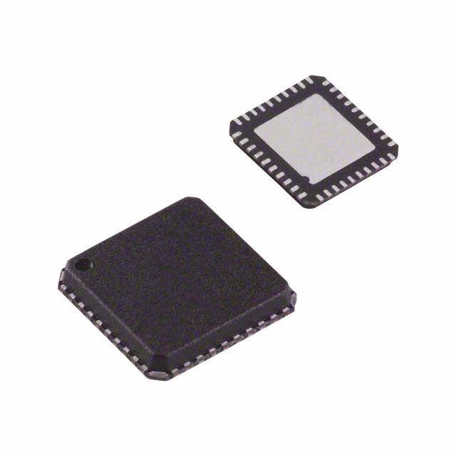
| 供应商器件封装 | 16-QFN(4x4) |
| 功能 | 解调器 |
| 包装 | 管件 |
| 噪声系数 | 12.8dB |
| 增益 | 4.3dB |
| 封装/外壳 | 16-WQFN 裸露焊盘 |
| 标准包装 | 91 |
| 电压-电源 | 4 V ~ 5.25 V |
| 电流-电源 | 150mA |


- 商务部:美国ITC正式对集成电路等产品启动337调查
- 曝三星4nm工艺存在良率问题 高通将骁龙8 Gen1或转产台积电
- 太阳诱电将投资9.5亿元在常州建新厂生产MLCC 预计2023年完工
- 英特尔发布欧洲新工厂建设计划 深化IDM 2.0 战略
- 台积电先进制程称霸业界 有大客户加持明年业绩稳了
- 达到5530亿美元!SIA预计今年全球半导体销售额将创下新高
- 英特尔拟将自动驾驶子公司Mobileye上市 估值或超500亿美元
- 三星加码芯片和SET,合并消费电子和移动部门,撤换高东真等 CEO
- 三星电子宣布重大人事变动 还合并消费电子和移动部门
- 海关总署:前11个月进口集成电路产品价值2.52万亿元 增长14.8%


PDF Datasheet 数据手册内容提取
LT5516 800MHz to 1.5GHz Direct Conversion Quadrature Demodulator FEATURES DESCRIPTIOU ■ Frequency Range: 800MHz to 1.5GHz The LT®5516 is an 800MHz to 1.5GHz direct conversion ■ High IIP3: 21.5dBm at 900MHz quadrature demodulator optimized for high linearity re- ■ High IIP2: 52dBm ceiver applications. It is suitable for communications ■ Noise Figure: 12.8dB at 900MHz receivers where an RF or IF signal is directly converted into ■ Conversion Gain: 4.3dB at 900MHz I and Q baseband signals with bandwidth up to 260MHz. ■ I/Q Gain Mismatch: 0.2dB The LT5516 incorporates balanced I and Q mixers, LO ■ Shutdown Mode buffer amplifiers and a precision, high frequency quadra- ■ 16-Lead QFN 4mm × 4mm Package ture generator. with Exposed Pad In an RF receiver, the high linearity of the LT5516 provides excellent spur-free dynamic range, even with fixed gain front end amplification. This direct conversion receiver APPLICATIOUS can eliminate the need for intermediate frequency (IF) signal processing, as well as the corresponding require- ■ Cellular/PCS/UMTS Infrastructure ments for image filtering and IF filtering. Channel filtering ■ High Linearity Direct Conversion I/Q Receiver can be performed directly at the outputs of the I and Q ■ High Linearity I/Q Demodulator channels. These outputs can interface directly to channel- select filters (LPFs) or to a baseband amplifier. LT, LTC and LTM are registered trademarks of Linear Technology Corporation. All other trademarks are the property of their respective owners. TYPICAL APPLICATIOU I/Q Output Power, IM3 vs 5V RF Input Power BPF BPF RF+ VCC LT5516 20 LNA IOUT+ LPF VGA 0 RF– 0° IOUT– ONE) –20 POUT DSP Bm/T LO INPUT LLOO+– 0°/90° 90° QQOOUUTT+– LPF VGA P, IM3 (dOUT –––468000 IM3 VTPffLRACLOF OC1= = ===2 9 5–580°1v91C09Md.9BHMmzHz fRF2 = 900.1MHz ENABLE EN –100 5516 F01 –18 –14 –10 –6 –2 2 6 RF INPUT POWER (dBm) Figure 1. High Signal-Level I/Q Demodulator for Wireless Infrastructure 5516 TA01 5516fa 1
LT5516 ABSOLUTE WAXIWUW RATIUGS PACKAGE/ORDER IUFORWATIOU (Note 1) TOP VIEW ORDER PART PEnoawbeler SVuopltpalgye V..o..l.t.a.g..e........................................................................................0.,5 V.5CVC +IOUT–IOUT+QOUT–QOUT NUMBER LO+ to LO– Differential Voltage ...............................±2V 16 15 14 13 LT5516EUF GND 1 12 VCC (+10dBm Equivalent) RF+ 2 11 LO– RF+ to RF– Differential Voltage................................±2V RF– 3 17 10 LO+ (+10dBm Equivalent) GND 4 9 VCC Operating Ambient Temperature..............–40°C to 85°C 5 6 7 8 UF PART Storage Temperature Range................. –65°C to 125°C VCC VCM EN VCC MARKING Maximum Junction Temperature..........................125°C UF PACKAGE 16-LEAD (4mm × 4mm) PLASTIC QFN 5516 EXPOSED PAD (PIN 17) IS GROUND (MUST BE SOLDERED TO PCB) TJMAX = 125°C, θJA = 38°C/W Order Options Tape and Reel: Add #TR Lead Free: Add #PBF Lead Free Tape and Reel: Add #TRPBF Lead Free Part Marking: http://www.linear.com/leadfree/ Consult LTC Marketing for parts specified with wider operating temperature ranges. AC ELECTRICAL CHARACTERISTICS TA = 25°C. VCC = 5V, EN = high, fRF1 = 899.9MHz, fRF2 = 900.1MHz, f = 901MHz, P = –10dBm unless otherwise noted. (Notes 2, 3) (Test circuit shown in Figure 2) LO LO PARAMETER CONDITIONS MIN TYP MAX UNITS Frequency Range 0.8 to 1.5 GHz LO Power –13 to –2 dBm Conversion Gain Voltage Gain, Load Impedance = 1k 2 4.3 dB Conversion Gain Variation vs Temperature –40°C to 85°C 0.01 dB/°C Noise Figure R1 = 8.2Ω 11.4 dB R1 = 3.3Ω, PLO = –5dBm 12.8 dB Input 3rd Order Intercept 2-Tone, –10dBm/Tone, R1 = 8.2Ω 17.0 dBm ∆f = 200kHz R1 = 3.3Ω, PLO = –5dBm 21.5 dBm Input 2nd Order Intercept Input = –10dBm R1 = 8.2Ω 46.0 dBm R1 = 3.3Ω, PLO = –5dBm 52.0 dBm Input 1dB Compression R1 = 8.2Ω 6.6 dBm Baseband Bandwidth 260 MHz I/Q Gain Mismatch (Note 4) 0.2 0.7 dB I/Q Phase Mismatch (Note 4) 1 degree Output Impedance Differential 120 Ω LO to RF Leakage –65 dBm RF to LO Isolation 57 dB 5516fa 2
LT5516 DC ELECTRICAL CHARACTERISTICS TA = 25°C. VCC = 5V unless otherwise noted. PARAMETER CONDITIONS MIN TYP MAX UNITS Supply Voltage 4 5.25 V Supply Current 80 117 150 mA Shutdown Current EN = Low 20 µA Turn-On Time 120 ns Turn-Off Time 650 ns EN = High (On) 1.6 V EN = Low (Off) 1.3 V EN Input Current VENABLE = 5V 2 µA Output DC Offset Voltage f = 901MHz, P = –10dBm 1 25 mV LO LO (⏐IOUT+ – IOUT–⏐, ⏐QOUT+ – QOUT–⏐) Output DC Offset Variation vs Temperature –40°C to 85°C 20 µV/°C Note 1: Stresses beyond those listed under Absolute Maximum Ratings Note 3: Specifications over the –40°C to 85°C temperature range are may cause permanent damage to the device. Exposure to any Absolute assured by design, characterization and correlation with statistical process Maximum Rating condition for extended periods may affect device control. reliability and lifetime. Note 4: Measured at P = –10dBm and output frequency = 1MHz. RF Note 2: Tests are performed as shown in the configuration of Figure 2 with R1 = 8.2Ω, unless otherwise noted. 5516fa 3
LT5516 TYPICAL PERFORW AU CE CHARACTERISTICS (Test circuit optimized for 900MHz operation as shown in Figure 2) Conv Gain, NF, IIP3 vs Supply Current vs Supply Voltage RF Input Frequency 160 25 R1 = 8.2Ω PLO = –10dBm A)140 TA = 85°C dBm) 20 TVRAC1 C == = 28 55.2°VΩC IIP3 RRENT (m112000 TTAA == 2–54°0C°C dB), IIP3 ( 15 SUPPLY CU 8600 GAIN (dB), NF ( 105 NCOFNV. GAIN 40 0 4 4.5 5 5.5 800 900 1000 1100 1200 1300 SUPPLY VOLTAGE (V) RF INPUT FREQUENCY (MHz) 5516 G01 5516 G02 I/Q Output Power, IM3 vs IIP2 vs RF Input Frequency RF Input Power 70 20 PLO = –10dBm fLO = 901MHz TA = 25°C VCC = 5V 60 VCC = 5V 0 R1 = 8.2Ω R1 = 8.2Ω E) OUTPUT POWER ON –20 m) 50 m/T IM3 B B IIP2 (d 40 , IM3 (dUT ––4600 TA = –40°C 30 PO TA = 85°C TA = 25°C –80 20 –100 800 900 1000 1100 1200 1300 –18 –14 –10 –6 –2 2 6 RF INPUT FREQUENCY (MHz) RF INPUT POWER (dBm) 5516 G03 5516 G04 I/Q Gain Mismatch vs RF Input Frequency 1.2 0.8 TA = –40°C B) d 0.4 H ( C T MA 0 MIS TA = 85°C TA = 25°C AIN –0.4 G PLO = –10dBm –0.8 fBB = 1MHz VCC = 5V R1 = 8.2Ω –1.2 800 900 1000 1100 1200 1300 1400 1500 RF INPUT FREQUENCY (MHz) 5516 G05 5516fa 4
LT5516 TYPICAL PERFORW AU CE CHARACTERISTICS (Test circuit optimized for 900MHz operation as shown in Figure 2) I/Q Phase Mismatch vs RF Input Frequency NF vs LO Input Power 6 18 4 16 fRF = 1300MHz EG) TA = –40°C 14 fRF = 1100MHz D 2 SE MISMATCH ( –02 TA = 85°C TA = 25°C NF (dB) 1120 fRF = 900MHz HA 8 P PLO = –10dBm –4 fBB = 1MHz 6 TA = 25°C VCC = 5V VCC = 5V R1 = 8.2Ω R1 = 8.2Ω –6 4 800 900 1000 1100 1200 1300 1400 1500 –14 –12 –10 –8 –6 –4 –2 RF INPUT FREQUENCY (MHz) LO INPUT POWER (dBm) 5516 G06 5516 G07 Conv Gain, IIP3 vs LO Input Power IIP2 vs LO Input Power 20 TA = 85°C 70 fLO = 901MHz 65 VCC = 5V Bm) 16 TA = –40°C 60 R1 = 8.2Ω 3 (d IIP3 TA = 25°C TA = 85°C GAIN (dB), IIP 128 fVRLCC1OCO == N= 89 V5.02 VG1ΩAMIHNz TA = 25°C IIP2 (dBm) 554505 TA = –40°C NV TA = –40°C TA = 25°C O 40 C 4 TA = 85°C 35 0 30 –14 –12 –10 –8 –6 –4 –2 –14 –12 –10 –8 –6 –4 –2 LO INPUT POWER (dBm) LO INPUT POWER (dBm) 5516 G08 5516 G09 Conv Gain, IIP3 vs Supply Voltage 20 TA = 85°C 3 (dBm) 16 IIP3 TA = –40°C TA = 25°C dB), IIP 12 fPLLOO = = 9 –0110MdHBzm N ( R1 = 8.2Ω GAI 8 CONV GAIN TA = 25°C NV TA = –40°C O C 4 TA = 85°C 0 4 4.5 5 5.5 SUPPLY VOLTAGE (V) 5516 G10 5516fa 5
LT5516 TYPICAL PERFORW AU CE CHARACTERISTICS (Test circuit optimized for 900MHz operation as shown in Figure 2) LO-RF Leakage vs LO Input Power RF-LO Isolation vs RF Input Power –55 80 TA = 25°C VCC = 5V fRF = 1100MHz R1 = 8.2Ω 70 –60 m) B) fRF = 1300MHz AKAGE (dB–65 ffRRFF == 910300M0MHHzz OLATION (d 6500 fRF = 900MHz F LE–70 O IS R L 40 LO- fRF = 1100MHz RF- –75 30 TA = 25°C VCC = 5V R1 = 8.2Ω –80 20 –14 –12 –10 –8 –6 –4 –2 –15 –10 –5 0 5 10 LO INPUT POWER (dBm) RF INPUT POWER (dBm) 5516 G11 5516 G12 RF, LO Port Return Loss vs Frequency Conv Gain vs Baseband Frequency 0 8 –5 RF 6 TA = –40°C LOSS (dB) ––1105 LO AIN (dB) 42 TA = 85°C RN V G TA = 25°C U N ET –20 CO 0 R –25 TA = 25°C –2 fLO = 1000MHz VCC = 5V VCC = 5V R1 = 8.2Ω R1 = 8.2Ω –30 –4 0 0.5 1 1.5 2 2.5 0.1 1 10 100 1000 FREQUENCY (GHz) BASEBAND FREQUENCY (MHz) 5516 G13 5516 G14 Conv Gain, NF, IIP3 vs R1 Supply Current, IIP2 vs R1 25 150 TA = 25°C PLO = –5dBm TA = 25°C PLO = –5dBm VCC = 5V fLO = 901MHz m)130 VCC = 5V fLO = 901MHz m) 20 dB dB), NF (dB), IIP3 (dB 1105 IINPF3 CURRENT (mA), IIP2 ( 1791000 SUPPLY CURRENT GAIN ( 5 CONV GAIN UPPLY 50 IIP2 S 0 30 3 4 5 6 7 8 9 3 4 5 6 7 8 9 R1 (Ω) R1 (Ω) 5516 G15 5516 G16 5516fa 6
LT5516 PIU FUUCTIOUS GND (Pins 1, 4): Ground Pin. LO+, LO– (Pins 10, 11): Differential Local Oscillator Input Pins. These pins are internally biased to 2.44V. They can RF+, RF– (Pins 2, 3): Differential RF Input Pins. These be driven single-ended by connecting one to an AC ground pins are internally biased to 1.54V. They must be driven through a 1000pF capacitor. However, differential input with a differential signal. An external matching network is drive is recommended to minimize LO feedthrough to the required for impedance transformation. RF input pins. V (Pins 5, 8, 9, 12): Power Supply Pins. These pins CC Q –, Q + (Pins 13, 14): Differential Baseband Output should be decoupled using 1000pF and 0.1µF capacitors. OUT OUT Pins of the Q-Channel. The internal DC bias voltage is V CC VCM (Pin 6): Common Mode and DC Return for the I-Mixer –0.68V for each pin. and Q-Mixer. An external resistor must be connected I –, I + (Pins 15, 16): Differential Baseband Output between this pin and ground to set the dc bias current of OUT OUT Pins of the I-Channel. The internal DC bias voltage is V the I/Q demodulator. CC –0.68V for each pin. EN (Pin 7): Enable Pin. When the input voltage is higher GROUND (Pin 17, Backside Contact): Ground Return for than 1.6V, the circuit is completely turned on. When the the Entire IC. This pin must be soldered to the printed input voltage is less than 1.3V, the circuit is turned off. circuit board ground plane. BLOCK DIAGRAW VCC VCC VCC VCC 5 8 9 12 I-MIXER LPF 16 IOUT+ RF AMP 15 IOUT– RF+ 2 LO BUFFERS 0°/90° RF– 3 LPF 14 QOUT+ VCM 6 Q-MIXER 13 QOUT– BIAS 7 1 4 17 10 11 EN GND GND LO+ LO– 5516 BD 5516fa 7
LT5516 TEST CIRCUITS C21 C18 OPT OPT J3 J5 IOUT– QOUT+ C19 C20 OPT OPT J4 J6 IOUT+ QOUT– T1 T2 J1 LDB31900M20C-416 +UT–UT+UT–UT LDB31900M20C-416 J2 RF 2 6 GND IO IO QO QO VCC 6 2 LO 1 L313nH RRFF+– LT5516 LLOO–+ L227nH 1 3 4 4 3 GND VCC C17 C1 VCC VCM EN VCC C1n5F 100Cp2F C10106pF 100pF 100pF VCC R3 1k EN C7 R1 R2 C6 C3 C4 1nF 3.3Ω 100k 1nF 0.1µF 2.2µF REFERENCE DESIGNATION VALUE SIZE PART NUMBER C1, C2, C16, C17 100pF 0402 AVX 04025C101JAT C5, C6, C7 1nF 0402 AVX 04025C102JAT C3 0.1µF 0402 AVX 0402ZD104KAT C4 2.2µF 3216 AVX TPSA225M010R1800 L1 33nH 0402 Murata LQP10A L2 27nH 0402 Murata LQP10A R1 3.3Ω 0402 R2 100k 0402 R3 1k 0402 T1, T2 1:4 Murata LDB31900M20C-416 5516 F02 Figure 2. 900MHz Evaluation Circuit Schematic Figure 3. Topside of Evaluation Board Figure 4. Bottom Side of Evaluation Board 5516fa 8
LT5516 APPLICATIOUS IUFORWATIOU The LT5516 is a direct I/Q demodulator targeting high An external resistor (R1) is connected to Pin 6 (V ) to set CM linearity receiver applications, including wireless infra- the optimum DC current for I/Q mixer linearity. The IIP3 can structure. It consists of an RF amplifier, I/Q mixers, a be improved with a smaller R1 at a price of slightly higher quadrature LO carrier generator and bias circuitry. NF and I . The RF performances of NF, IIP3 and IIP2 vs CC R1 are shown in the Typical Performance Characteristics. The RF signal is applied to the inputs of the RF amplifier and is then demodulated into I/Q baseband signals using LO Input Port quadrature LO signals. The quadrature LO signals are internally generated by precision 90° phase shifters. The The LO inputs (Pins 10,11) should be driven differentially demodulated I/Q signals are lowpass filtered internally to minimize LO feedthrough to the RF port. This can be with a –3dB bandwidth of 265MHz. The differential out- accomplished by means of a single-ended to differential puts of the I-channel and Q-channel are well matched in conversion as shown in Figure 2. L4, the 27nH shunt amplitude; their phases are 90° apart. inductor, serves to tune out the capacitive component of the LO differential input. The resonance frequency of the RF Input Port inductor should be greater than the operating frequency. A 1:4 transformer is used on the demo board to match the Differential drive is highly recommended for the RF inputs 200Ω on-chip resistance to a 50Ω source. Figure 6 shows to minimize the LO feedthrough to the RF port and to the LO input equivalent circuit and the associated match- maximize gain. (See Figure 2.) A 1:4 transformer is used ing network. on the demonstration board for wider bandwidth match- ing. To assure good NF and maximize the demodulator Single-ended to differential conversion at the LO inputs gain, a low loss transformer is employed. Shunt inductor can also be implemented using a discrete L-C circuit to L1, with high resonance frequency, is required for proper produce a balanced waveform without a transformer. impedance matching. Single-ended to differential conver- An alternative solution is a simple single-ended termina- sion can also be implemented using narrow band, discrete tion. However, the LO feedthrough to RF may be degraded. L-C circuits to produce the required balanced waveforms Either LO+ or LO– input can be terminated to a 50Ω source at the RF+ and RF– inputs.The differential impedance of with a matching circuit, while the other input is connected the RF inputs is listed in Table 1. to ground through a 100pF bypass capacitor. Table 1. RF Input Differential Impedance Table 2 shows the differential input impedance of the LO FREQUENCY DIFFERENTIAL INPUT DIFFERENTIAL S11 input port. (MHz) IMPEDANCE (Ω) MAG ANGLE (°) Table 2. LO Input Differential Impedance 800 169.7-j195.2 0.779 –16.9 900 156.1-j181.8 0.766 –18.3 FREQUENCY DIFFERENTIAL INPUT DIFFERENTIAL S11 (MHz) IMPEDANCE (Ω) MAG ANGLE (°) 1000 145.6-j170.0 0.753 –19.6 800 118.4-j65.1 0.552 –22.5 1100 137.3-j160.0 0.740 –20.9 900 110.1-j66.7 0.517 –25.4 1200 130.7-j152.1 0.729 –21.9 1000 102.2-j67.5 0.512 –28.5 1300 124.9-j144.7 0.718 –23.0 1100 94.6-j67.2 0.505 –31.8 1400 119.9-j138.3 0.707 –24.0 1200 87.5-j66.1 0.498 –35.0 1500 115.7-j133.1 0.698 –24.9 1300 80.8-j64.4 0.490 –38.3 The RF+ and RF– inputs (Pins 2, 3) are internally biased at 1400 74.7-j62.1 0.480 –42.0 2.44V. These two pins should be DC blocked when con- 1500 69.3-j59.4 0.469 –45.8 nected to ground or other matching components. The RF input equivalent circuit is shown in Figure 5. 5516fa 9
LT5516 APPLICATIOUS IUFORWATIOU I-Channel and Q-Channel Outputs The phase relationship between the I-channel output sig- nal and Q-channel output signal is fixed. When the LO Each of the I-channel and Q-channel outputs is internally input frequency is larger (or smaller) than the RF input connected to V though a 60Ω resistor. The output dc CC frequency, the Q-channel outputs (Q +, Q –) lead (or bias voltage is V – 0.68V. The outputs can be DC coupled OUT OUT CC lag) I-channel outputs (I +, I –) by 90°. or AC coupled to the external loads. The differential output OUT OUT impedance of the demodulator is 120Ω in parallel with a When AC output coupling is used, the resulting highpass 5pF internal capacitor, forming a lowpass filter with a filter’s –3dB roll-off frequency is defined by the R-C –3dB corner frequency at 265MHz. R (the single- constant of the blocking capacitor and R , assuming LOAD LOAD ended load resistance) should be larger than 600Ω to R > 600Ω. LOAD assure full gain. The gain is reduced by 20 • log(1 + 120Ω/ Care should be taken when the demodulator’s outputs are R ) in dB when the differential output is terminated by LOAD DC coupled to the external load, to make sure that the I/Q R . For instance, the gain is reduced by 6.85dB when LOAD mixers are biased properly. If the current drain from the each output pin is connected to a 50Ω load (100Ω differ- outputs exceeds 6mA, there can be significant degrada- ential load). The output should be taken differentially (or tion of the linearity performance. Each output can sink no by using differential-to-single-ended conversion) for best more than 13mA when the outputs are connected to an RF performance, including NF and IM2. external load with a DC voltage higher than V – 0.68V. CC The I/Q output equivalent circuit is shown in Figure 7. LT5516 VCC T1 J1 LDB31900M20C-416 RF+ 1.54V RF 2 2 6 1 L1 1k 33nH 3 4 RF– 3 1.54V C1 1nF NOTE: NO CONNECTION REQUIRED 5516 F05 ACCORDING TO BALUN TRANSFORMER MANUFACTURER Figure 5. RF Input Equivalent Circuit with External Matching 5516fa 10
LT5516 APPLICATIOUS IUFORWATIOU VCC VCC 60Ω 60Ω 60Ω 60Ω T2 IOUT+ J2 LDB31900M20C-416 16 LO+ 2.44V LO 10 IOUT– 2 6 15 1 L247nH 200Ω 5pF QOUT+ 14 3 4 11 LO– QOUT– 2.44V 13 C2 5pF 1nF NOTE: NO CONNECTION REQUIRED ACCORDING TO BALUN TRANSFORMER 5516 F06 MANUFACTURER 5516 F07 Figure 6. LO Input Equivalent Circuit with External Matching Figure 7. I/Q Output Equivalent Circuit PACKAGE DESCRIPTIOU UF Package 16-Lead Plastic QFN (4mm × 4mm) (Reference LTC DWG # 05-08-1692) 0.72 ±0.05 4.35 ± 0.05 2.15 ± 0.05 2.90 ± 0.05 (4 SIDES) PACKAGE OUTLINE 0.30 ±0.05 0.65 BSC RECOMMENDED SOLDER PAD PITCH AND DIMENSIONS BOTTOM VIEW—EXPOSED PAD PIN 1 NOTCH R = 0.20 TYP 4.00 ± 0.10 0.75 ± 0.05 R = 0.115 OR 0.35 × 45° CHAMFER (4 SIDES) TYP 15 16 PIN 1 0.55 ± 0.20 TOP MARK (NOTE 6) 1 2 2.15 ± 0.10 (4-SIDES) (UF16) QFN 1004 0.200 REF 0.30 ± 0.05 0.00 – 0.05 0.65 BSC NOTE: 1. DRAWING CONFORMS TO JEDEC PACKAGE OUTLINE MO-220 VARIATION (WGGC) 5. EXPOSED PAD SHALL BE SOLDER PLATED 2. DRAWING NOT TO SCALE 6. SHADED AREA IS ONLY A REFERENCE FOR PIN 1 LOCATION 3. ALL DIMENSIONS ARE IN MILLIMETERS ON THE TOP AND BOTTOM OF PACKAGE 4. DIMENSIONS OF EXPOSED PAD ON BOTTOM OF PACKAGE DO NOT INCLUDE MOLD FLASH. MOLD FLASH, IF PRESENT, SHALL NOT EXCEED 0.15mm ON ANY SIDE 5516fa Information furnished by Linear Technology Corporation is believed to be accurate and reliable. 11 However, no responsibility is assumed for its use. Linear Technology Corporation makes no represen- tation that the interconnection of its circuits as described herein will not infringe on existing patent rights.
LT5516 RELATED PARTS PART NUMBER DESCRIPTION COMMENTS RF Power Controllers LTC1757A RF Power Controller Multiband GSM/DCS/GPRS Mobile Phones LTC1758 RF Power Controller Multiband GSM/DCS/GPRS Mobile Phones LTC1957 RF Power Controller Multiband GSM/DCS/GPRS Mobile Phones LTC4400 SOT-23 RF PA Controller Multiband GSM/DCS/GPRS Phones, 45dB Dynamic Range, 450kHz Loop BW LTC4401 SOT-23 RF PA Controller Multiband GSM/DCS/GPRS Phones, 45dB Dynamic Range, 250kHz Loop BW LTC4403 RF Power Controller for EDGE/TDMA Multiband GSM/GPRS/EDGE Mobile Phones LT5500 RF Front End Dual LNA gain Setting +13.5dB/–14dB at 2.5GHz, Double-Balanced Mixer, 1.8V ≤ VSUPPLY ≤ 5.25V LT5502 400MHz Quadrature Demodulator with RSSI 1.8V to 5.25V Supply, 70MHz to 400MHz IF, 84dB Limiting Gain, 90dB RSSI Range LT5503 1.2GHz to 2.7GHz Direct IQ Modulator and 1.8V to 5.25V Supply, Four-Step RF Power Control, 120MHz Modulation Bandwidth Up Converting Mixer LT5504 800MHz to 2.7GHz RF Measuring Receiver 80dB Dynamic Range, Temperature Compensated, 2.7V to 5.5V Supply LTC5505 300MHz to 3.5GHz RF Power Detector >40dB Dynamic Range, Temperature Compensated, 2.7V to 6V Supply LT5506 500MHz Quadrature IF Demodulator with VGA 1.8V to 5.25V Supply, 40MHz to 500MHz IF, –4dB to 57dB Linear Power Gain LTC5507 100kHz to 1GHz RF Power Detector 48dB Dynamic Range, Temperature Compensated, 2.7V to 6V Supply LTC5508 300MHz to 7GHz RF Power Detector SC70 Package LTC5509 300MHz to 3GHz RF Power Detector 36dB Dynamic Range, SC70 Package LT5511 High Signal Level Up Converting Mixer RF Output to 3GHz, 17dBm IIP3, Integrated LO Buffer LT5512 High Signal Level Down Converting Mixer DC-3GHz, 20dBm IIP3, Integrated LO Buffer 5516fa 12 Linear Technology Corporation LT 0406 REV A • PRINTED IN USA 1630 McCarthy Blvd., Milpitas, CA 95035-7417 (408) 432-1900 ● FAX: (408) 434-0507 ● www.linear.com © LINEAR TECHNOLOGY CORPORATION 2003
Mouser Electronics Authorized Distributor Click to View Pricing, Inventory, Delivery & Lifecycle Information: A nalog Devices Inc.: LT5516EUF LT5516EUF#TRPBF LT5516EUF#TR LT5516EUF#PBF