ICGOO在线商城 > 集成电路(IC) > 数据采集 - ADCs/DAC - 专用型 > AD974BRZ
 Datasheet下载
- 型号: AD974BRZ
- 制造商: Analog
- 库位|库存: xxxx|xxxx
- 要求:
| 数量阶梯 | 香港交货 | 国内含税 |
| +xxxx | $xxxx | ¥xxxx |
查看当月历史价格
查看今年历史价格
AD974BRZ产品简介:
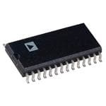
ICGOO电子元器件商城为您提供AD974BRZ由Analog设计生产,在icgoo商城现货销售,并且可以通过原厂、代理商等渠道进行代购。 AD974BRZ价格参考¥406.01-¥475.60。AnalogAD974BRZ封装/规格:数据采集 - ADCs/DAC - 专用型, 数据采集系统(DAS) 16 b 200k 串行 28-SOIC。您可以下载AD974BRZ参考资料、Datasheet数据手册功能说明书,资料中有AD974BRZ 详细功能的应用电路图电压和使用方法及教程。
AD974BRZ是由Analog Devices Inc.生产的一款专用型数据采集器件,主要用于数模转换(DAC)应用。该型号属于AD974系列,具有高精度、低功耗和高集成度的特点,适用于需要高性能信号处理的场合。

 应用场景:

1. 通信系统:
   AD974BRZ广泛应用于通信领域,特别是在无线基站、软件定义无线电(SDR)、雷达系统等场景中。它能够将数字信号高效地转换为模拟信号,支持高速数据传输和复杂的调制方案。其低噪声和高线性度特性使其在多载波通信系统中表现出色,确保了信号的完整性和可靠性。

2. 测试与测量设备:
   在精密测试仪器中,如频谱分析仪、示波器、信号发生器等,AD974BRZ用于生成高精度的模拟信号。它的高分辨率和快速响应时间使得这些设备能够在广泛的频率范围内进行精确测量。此外,它还支持多种输出模式,适应不同的测试需求。

3. 医疗设备:
   医疗成像设备(如超声波、CT扫描仪)和生理信号监测系统(如心电图、脑电图)也依赖于AD974BRZ的高性能DAC功能。它能够将数字处理后的医学图像或生理信号准确地转换为模拟信号,以供显示或进一步处理。其低功耗和高稳定性特性对于便携式医疗设备尤为重要。

4. 工业自动化与控制:
   在工业控制系统中,AD974BRZ用于实现精确的模拟信号输出,驱动执行器、传感器或其他外围设备。例如,在过程控制、电机控制、伺服系统等领域,它能够提供稳定的电压或电流输出,确保系统的正常运行。其内置的校准功能还可以减少外部元件的需求,简化设计并提高可靠性。

5. 音频处理:
   高保真音频设备(如专业音响、录音设备)也使用AD974BRZ来实现高质量的数模转换。它能够提供纯净的音频信号输出,减少失真和噪声,满足专业音频领域的严格要求。

总之,AD974BRZ凭借其优异的性能和灵活性,适用于各种对信号质量有较高要求的应用场景,尤其是在通信、测试测量、医疗和工业自动化等领域表现突出。
| 参数 | 数值 |
| 产品目录 | 集成电路 (IC)半导体 |
| 描述 | IC DAS 16BIT 4CH 200KSPS 28SOIC模数转换器 - ADC 4CH 16-Bit 200 kSPS |
| 产品分类 | |
| 品牌 | Analog Devices Inc |
| 产品手册 | |
| 产品图片 |
|
| rohs | 符合RoHS无铅 / 符合限制有害物质指令(RoHS)规范要求 |
| 产品系列 | 数据转换器IC,模数转换器 - ADC,Analog Devices AD974BRZ- |
| 数据手册 | |
| 产品型号 | AD974BRZ |
| 产品目录页面 | |
| 产品种类 | 模数转换器 - ADC |
| 供应商器件封装 | 28-SOIC W |
| 信噪比 | 85 dB |
| 分辨率 | 16 bit |
| 分辨率(位) | 16 b |
| 包装 | 管件 |
| 商标 | Analog Devices |
| 安装类型 | 表面贴装 |
| 安装风格 | SMD/SMT |
| 封装 | Tube |
| 封装/外壳 | 28-SOIC(0.295",7.50mm 宽) |
| 封装/箱体 | SOIC-28 |
| 工作温度 | -40°C ~ 85°C |
| 工作电源电压 | 5 V |
| 工厂包装数量 | 27 |
| 接口类型 | Serial (SPI) |
| 数据接口 | 串行 |
| 最大功率耗散 | 120 mW |
| 最大工作温度 | + 85 C |
| 最小工作温度 | - 40 C |
| 标准包装 | 1 |
| 电压-电源 | 4.75 V ~ 5.25 V |
| 电压参考 | Internal, External |
| 电压源 | 模拟和数字 |
| 类型 | 数据采集系统(DAS) |
| 系列 | AD974 |
| 结构 | SAR |
| 转换器数量 | 1 |
| 转换速率 | 200 kS/s |
| 输入类型 | Single-Ended |
| 通道数量 | 4 Channel |
| 配用 | /product-detail/zh/EVAL-AD974CB/EVAL-AD974CB-ND/624979 |
| 采样率(每秒) | 200k |


- 商务部:美国ITC正式对集成电路等产品启动337调查
- 曝三星4nm工艺存在良率问题 高通将骁龙8 Gen1或转产台积电
- 太阳诱电将投资9.5亿元在常州建新厂生产MLCC 预计2023年完工
- 英特尔发布欧洲新工厂建设计划 深化IDM 2.0 战略
- 台积电先进制程称霸业界 有大客户加持明年业绩稳了
- 达到5530亿美元!SIA预计今年全球半导体销售额将创下新高
- 英特尔拟将自动驾驶子公司Mobileye上市 估值或超500亿美元
- 三星加码芯片和SET,合并消费电子和移动部门,撤换高东真等 CEO
- 三星电子宣布重大人事变动 还合并消费电子和移动部门
- 海关总署:前11个月进口集成电路产品价值2.52万亿元 增长14.8%


PDF Datasheet 数据手册内容提取
a 4-Channel, 16-Bit, 200 kSPS Data Acquisition System AD974 FEATURES FUNCTIONAL BLOCK DIAGRAM Fast 16-Bit ADC with 200 kSPS Throughput Four Single-Ended Analog Input Channels PWRD BIP CAP REF VDIG VANA Single +5 V Supply Operation Input Ranges: 0 V to +4 V, 0 V to +5 V and 610 V REF 2.5V 120 mW Max Power Dissipation BUFF REFERENCE Power-Down Mode 50 mW V1A RESISTIVE Choice of External or Internal 2.5 V Reference V1B NETWORK AD974 On-Chip Clock EXT/INT Power-Down Mode VV22AB RNEESTWISOTIRVKE SWITCHED 16 DATACLK 4 TO 1 CAP ADC SERIAL DATA MUX INTERFACE + R/C V3A RESISTIVE LATCH V3B NETWORK CS CLOCK SYNC V4A RESISTIVE EN V4B NETWORK CONTROL LOGIC & GENERAL DESCRIPTION CALIBRATION CIRCUITRY The AD974 is a four-channel, data acquisition system with a serial interface. The part contains an input multiplexer, a high- AGND1 AGND2 A0 A1WR1WR2 BUSY DGND speed 16-bit sampling ADC and a +2.5 V reference. All of this operates from a single +5 V power supply that also has a power- down mode. The part will accommodate 0 V to +4 V, 0 V to +5 V or – 10 V analog input ranges. PRODUCT HIGHLIGHTS 1. The AD974 is a complete data acquisition system combining The interface is designed for an efficient transfer of data while a four-channel multiplexer, a 16-bit sampling ADC and a requiring a low number of interconnects. +2.5 V reference on a single chip. The AD974 is comprehensively tested for ac parameters such as 2. The part operates from a single +5 V supply and also has a SNR and THD, as well as the more traditional parameters of power-down feature. offset, gain and linearity. 3. Interfacing to the AD974 is simple with a low number of The AD974 is fabricated on Analog Devices’ BiCMOS process, interconnect signals. which has high performance bipolar devices along with CMOS 4. The AD974 is comprehensively specified for ac parameters transistors. such as SNR and THD, as well as dc parameters such as The AD974 is available in 28-lead DIP, SOIC and SSOP linearity and offset and gain errors. packages. REV. A Information furnished by Analog Devices is believed to be accurate and reliable. However, no responsibility is assumed by Analog Devices for its use, nor for any infringements of patents or other rights of third parties One Technology Way, P.O. Box 9106, Norwood, MA 02062-9106, U.S.A. which may result from its use. No license is granted by implication or Tel: 781/329-4700 World Wide Web Site: http://www.analog.com otherwise under any patent or patent rights of Analog Devices. Fax: 781/326-8703 © Analog Devices, Inc., 1999
AD974–SPECIFICATIONS (–408C to +858C, f = 200 kHz, V = V = +5 V, unless otherwise noted) S DIG ANA A Grade B Grade Parameter Conditions Min Typ Max Min Typ Max Units RESOLUTION 16 16 Bits ANALOG INPUT Voltage Range – 10 V, 0 V to +4 V, 0 V to +5 V (See Table I) Impedance Channel On or Off (See Table I) Sampling Capacitance 40 40 pF THROUGHPUT SPEED Complete Cycle (Acquire and Convert) 5 5 m s Throughput Rate 200 200 kHz DC ACCURACY Integral Linearity Error – 3 – 2.0 LSB1 Differential Linearity Error –2 +3 –1 +1.75 LSB No Missing Codes 15 16 Bits Transition Noise2 1.0 1.0 LSB Full-Scale Error3 Internal Reference – 0.5 – 0.25 % Full-Scale Error Drift Internal Reference – 7 – 7 ppm/(cid:176) C Full-Scale Error Ext. REF = +2.5 V – 0.5 – 0.25 % Full-Scale Error Drift Ext. REF = +2.5 V – 2 – 2 ppm/(cid:176) C Bipolar Zero Error Bipolar Range – 10 – 10 mV Bipolar Zero Error Drift Bipolar Range – 2 – 2 ppm/(cid:176) C Unipolar Zero Error Unipolar Ranges – 10 – 10 mV Unipolar Zero Error Drift Unipolar Ranges – 2 – 2 ppm/(cid:176) C Channel-to-Channel Matching – 0.1 – 0.05 % FSR Recovery to Rated Accuracy After Power-Down4 2.2 m F to CAP 1 1 ms Power Supply Sensitivity V = V = V V = 5 V – 5% – 8 – 8 LSB ANA DIG D D AC ACCURACY Spurious Free Dynamic Range f = 20 kHz 90 96 dB5 IN Total Harmonic Distortion f = 20 kHz –90 –96 dB IN Signal-to-(Noise+Distortion) f = 20 kHz 83 85 dB IN –60 dB Input 27 28 dB Signal-to-Noise f = 20 kHz 83 85 dB IN Channel-to-Channel Isolation f = 20 kHz –110 –100 –110 –100 dB IN Full Power Bandwidth6 1 1 MHz –3 dB Input Bandwidth 2.7 2.7 MHz SAMPLING DYNAMICS Aperture Delay 40 40 ns Transient Response Full-Scale Step 1 1 m s Overvoltage Recovery7 150 150 ns REFERENCE Internal Reference Voltage 2.48 2.5 2.52 2.48 2.5 2.52 V Internal Reference Source Current 1 1 m A External Reference Voltage Range for Specified Linearity 2.3 2.5 2.7 2.3 2.5 2.7 V External Reference Current Drain Ext. REF = +2.5 V 100 100 m A DIGITAL INPUTS Logic Levels V –0.3 +0.8 –0.3 +0.8 V IL V +2.0 V + 0.3 +2.0 V + 0.3 V IH DIG DIG I – 10 – 10 m A IL I – 10 – 10 m A IH –2– REV. A
AD974 A Grade B Grade Parameter Conditions Min Typ Max Min Typ Max Units DIGITAL OUTPUTS Data Format Serial 16 Bits Data Coding Straight Binary V I = 1.6 mA +0.4 +0.4 V OL SINK V I = 500 m A +4 +4 V OH SOURCE Output Capacitance High-Z State 15 15 pF Leakage Current High-Z State V = 0 V to V – 5 – 5 m A OUT DIG POWER SUPPLIES Specified Performance V +4.75 +5 +5.25 +4.75 +5 +5.25 V DIG V +4.75 +5 +5.25 +4.75 +5 +5.25 V ANA I 4.5 4.5 mA DIG I 14 14 mA ANA Power Dissipation PWRD LOW 120 120 mW PWRD HIGH 50 50 m W TEMPERATURE RANGE Specified Performance T to T –40 +85 –40 +85 (cid:176) C MIN MAX NOTES 1LSB means Least Significant Bit. With a – 10 V input, one LSB is 305 m V. 2Typical rms noise at worst case transitions and temperatures. 3Full-Scale Error is expressed as the % difference between the actual full-scale code transition voltage and the ideal full-scale transition voltage, and includes the effect of offset error. For bipolar input, the Full-Scale Error is the worst case of either the –Full-Scale or +Full-Scale code transition voltage errors. For unipolar input ranges, Full-Scale Error is with respect to the +Full-Scale code transition voltage. 4External 2.5 V reference connected to REF. 5All specifications in dB are referred to a full-scale – 10 V input. 6Full-Power Bandwidth is defined as full-scale input frequency at which Signal-to-(Noise + Distortion) degrades to 60 dB, or 10 bits of accuracy. 7Recovers to specified performance after a 2 · FS input overvoltage. Specifications subject to change without notice. TIMING SPECIFICATIONS (f = 200 kHz, V = V = +5 V, –408C to +858C) S DIG ANA Parameter Symbol Min Typ Max Units Convert Pulsewidth t 50 ns 1 R/C, CS to BUSY Delay t 100 ns 2 BUSY LOW Time t 4.0 m s 3 BUSY Delay after End of Conversion t 50 ns 4 Aperture Delay t 40 ns 5 Conversion Time t 3.8 4.0 m s 6 Acquisition Time t 1.0 m s 7 Throughput Time t + t 5 m s 6 7 R/C Low to DATACLK Delay t 220 ns 8 DATACLK Period t 220 ns 9 DATA Valid Setup Time t 50 ns 10 DATA Valid Hold Time t 20 ns 11 EXT. DATACLK Period t 66 ns 12 EXT. DATACLK HIGH t 20 ns 13 EXT. DATACLK LOW t 30 ns 14 R/C, CS to EXT. DATACLK Setup Time t 20 t + 5 ns 15 12 R/C to CS Setup Time t 10 ns 16 EXT. DATACLK to SYNC Delay t 15 66 ns 17 EXT. DATACLK to DATA Valid Delay t 25 66 ns 18 CS to EXT. DATACLK Rising Edge Delay t 10 ns 19 Previous DATA Valid after CS, R/C Low t 3.5 m s 20 BUSY to EXT. DATACLK Setup Time t 5 ns 21 Final EXT. DATACLK to BUSY Rising Edge t 1.7 m s 22 A0, A1 to WR1, WR2 Setup Time t 10 ns 23 A0, A1 to WR1, WR2 Hold Time t 10 ns 24 WR1, WR2 Pulsewidth t 50 ns 25 Specifications subject to change without notic e. REV. A –3–
AD974 ABSOLUTE MAXIMUM RATINGS1 PIN CONFIGURATION Analog Inputs SOIC, DIP AND SSOP VxA, VxB . . . . . . . . . . . . . . . . . . . . . . . . . . . . . . . . . .– 25 V CAP . . . . . . . . . . . . . . . .+V + 0.3 V to AGND2 – 0.3 V ANA REF . . . . . . . . . . . . . . . . . . . . Indefinite Short to AGND2, AGND1 1 28 V2B Momentary Short to V ANA V3A 2 27 V2A Ground Voltage Differences V3B 3 26 V1B DGND, AGND1, AGND2 . . . . . . . . . . . . . . . . . . . – 0.3 V V4A 4 25 V1A Supply␣Voltages V4B 5 24 VANA V . . . . . . . . . . . . . . . . . . . . . . . . . . . . . . . . . . . . . .+7 V ANA BIP 6 23 A0 V to V . . . . . . . . . . . . . . . . . . . . . . . . . . . . . . . .– 7 V AD974 DIG ANA CAP 7 TOP VIEW 22 A1 V . . . . . . . . . . . . . . . . . . . . . . . . . . . . . . . . . . . . . .+7 V DIG REF 8 (Not to Scale) 21 BUSY Digital Inputs . . . . . . . . . . . . . . . . . . .–0.3 V to V + 0.3 V DIG AGND2 9 20 CS Internal␣Power␣Dissipation2 R/C 10 19 WR1 PDIP (N), SOIC (R), SSOP (RS) . . . . . . . . . . . . . 700 mW Junction Temperature . . . . . . . . . . . . . . . . . . . . . . . . .+150(cid:176) C VDIG 11 18 WR2 PWRD 12 17 DATA Storage Temperature Range N, R . . . . . . . . –65(cid:176) C to +150(cid:176) C EXT/INT 13 16 DATACLK Lead Temperature Range DGND 14 15 SYNC (Soldering␣10␣sec) . . . . . . . . . . . . . . . . . . . . . . . . . .+300(cid:176) C NOTES 1Stresses above those listed under Absolute Maximum Ratings may cause perma- nent damage to the device. This is a stress rating only; functional operation of the device at these or any other conditions above those indicated in the operational section of this specification is not implied. Exposure to absolute maximum rating 1.6mA IOL conditions for extended periods may affect device reliability. 2Specification is for device in free air: 28-Lead PDIP: q JA = 100(cid:176)C/W, q JC = 31(cid:176)C/W TO OUTPUT +1.4V 28-Lead SOIC: q = 75(cid:176)C/W, q = 24(cid:176)C/W PIN 28-Lead SSOP: q JA = 109(cid:176)C/W, JqC = 39(cid:176)C/W CL JA JC 100pF 500mA IOH Figure 1.Load Circuit for Digital Interface Timing ORDERING GUIDE Temperature Package Package Model Range Max INL Min S/(N+D) Description Options AD974AN –40(cid:176) C to +85(cid:176) C – 3.0 LSB 83 dB 28-Lead Plastic DIP N-28B AD974BN –40(cid:176) C to +85(cid:176) C – 2.0 LSB 85 dB 28-Lead Plastic DIP N-28B AD974AR –40(cid:176) C to +85(cid:176) C – 3.0 LSB 83 dB 28-Lead SOIC R-28 AD974BR –40(cid:176) C to +85(cid:176) C – 2.0 LSB 85 dB 28-Lead SOIC R-28 AD974ARS –40(cid:176) C to +85(cid:176) C – 3.0 LSB 83 dB 28-Lead SSOP RS-28 AD974BRS –40(cid:176) C to +85(cid:176) C – 2.0 LSB 85 dB 28-Lead SSOP RS-28 CAUTION ESD (electrostatic discharge) sensitive device. Electrostatic charges as high as 4000 V readily WARNING! accumulate on the human body and test equipment and can discharge without detection. Although the AD974 features proprietary ESD protection circuitry, permanent damage may occur on devices subjected to high energy electrostatic discharges. Therefore, proper ESD ESD SENSITIVE DEVICE precautions are recommended to avoid performance degradation or loss of functionality. –4– REV. A
AD974 PIN FUNCTION DESCRIPTIONS Pin No. Mnemonic Description 1 AGND1 Analog Ground. Used as the ground reference point for the REF pin. 2–5, 25–28 VxA, VxB Analog Input. Refer to Table I for input range configuration. 6 BIP Bipolar Offset. Connect VxA inputs to provide Bipolar input range. 7 CAP Reference Buffer Output. Connect a 2.2 m F tantalum capacitor between CAP and Analog Ground. 8 REF Reference Input/Output. The internal +2.5 V reference is available at this pin. Alternatively an external reference can be used to override the internal reference. In either case, connect a 2.2 m F tantalum capacitor between REF and Analog Ground. 9 AGND2 Analog Ground. 10 R/C Read/Convert Input. Used to control the conversion and read modes. With CS LOW, a falling edge on R/C holds the analog input signal internally and starts a conversion; a rising edge enables the transmission of the conversion result. 11 V Digital Power Supply. Nominally +5 V. DIG 12 PWRD Power-Down Input. When set to a logic HIGH, power consumption is reduced and conversions are inhibited. The conversion result from the previous conversion is stored in the onboard shift register. 13 EXT/INT Digital select input for choosing the internal or an external data clock. With EXT/INT tied LOW, after initiating a conversion, 16 DATACLK pulses transmit the previous conversion result as shown in Figure 3. With EXT/INT set to a Logic HIGH, output data is synchronized to an external clock signal connected to the DATACLK input. Data is output as indicated in Figure 4 through Figure 9. 14 DGND Digital Ground. 15 SYNC Digital output frame synchronization for use with an external data clock (EXT/INT = Logic HIGH). When a read sequence is initiated, a pulse one DATACLK period wide is output synchronous to the external data clock. 16 DATACLK Serial data clock input or output, dependent upon the logic state of the EXT/INT pin. When using the internal data clock (EXT/INT = Logic LOW), a conversion start sequence will initiate transmission of 16 DATACLK periods. Output data is synchronous to this clock and is valid on both its rising and falling edges (Figure 3). When using an external data clock (EXT/INT = Logic HIGH), the CS and R/C signals control how conversion data is accessed. 17 DATA The serial data output is synchronized to DATACLK. Conversion results are stored in an on- chip register. The AD974 provides the conversion result, MSB first, from its internal shift regis- ter. When using the internal data clock (EXT/INT = Logic LOW), DATA is valid on both the rising and falling edges of DATACLK. Using an external data clock (EXT/INT = Logic HIGH) allows previous conversion data to be accessed during a conversion (Figures 5, 7 and 9) or the conversion result can be accessed after the completion of a conversion (Figures 4, 6 and 8). 18, 19 WR1, WR2 Multiplexer Write Inputs. These inputs are internally ORed to generate the mux latch inputs. The latch is transparent when WR1 and WR2 are tied low. 20 CS Chip Select Input. With R/C LOW, a falling edge on CS will initiate a conversion. With R/C HIGH, a falling edge on CS will enable the serial data output sequence. 21 BUSY Busy Output. Goes LOW when a conversion is started, and remains LOW until the conversion is completed and the data is latched into the on-chip shift register. 22, 23 A1, A0 Address multiplexer inputs latched with the WR1, WR2 inputs. A1 A0 Data Available from Channel 0 0 AIN 1 0 1 AIN 2 1 0 AIN 3 1 1 AIN 4 24 V Analog Power Supply. Nominally +5 V. ANA REV. A –5–
AD974 DEFINITION OF SPECIFICATIONS SPURIOUS FREE DYNAMIC RANGE INTEGRAL NONLINEARITY ERROR (INL) The difference, in decibels (dB), between the rms amplitude of Linearity error refers to the deviation of each individual code the input signal and the peak spurious signal. from a line drawn from “negative full scale” through “positive full scale.” The point used as “negative full scale” occurs 1/2 LSB TOTAL HARMONIC DISTORTION (THD) before the first code transition. “Positive full scale” is defined as THD is the ratio of the rms sum of the first six harmonic com- a level 1 1/2 LSB beyond the last code transition. The deviation ponents to the rms value of a full-scale input signal and is ex- is measured from the middle of each particular code to the true pressed in decibels. straight line. SIGNAL TO (NOISE AND DISTORTION) (S/[N+D]) RATIO DIFFERENTIAL NONLINEARITY ERROR (DNL) S/(N+D) is the ratio of the rms value of the measured input In an ideal ADC, code transitions are 1 LSB apart. Differential signal to the rms sum of all other spectral components below nonlinearity is the maximum deviation from this ideal value. It the Nyquist frequency, including harmonics but excluding dc. is often specified in terms of resolution for which no missing The value for S/(N+D) is expressed in decibels. codes are guaranteed. FULL POWER BANDWIDTH FULL-SCALE ERROR The full power bandwidth is defined as the full-scale input fre- The last + transition (from 011...10 to 011...11) should quency at which the S/(N+D) degrades to 60 dB, 10 bits of occur for an analog voltage 1 1/2 LSB below the nominal full accuracy. scale (9.9995422 V for a – 10 V range). The full-scale error is the deviation of the actual level of the last transition from the APERTURE DELAY ideal level. Aperture delay is a measure of the acquisition performance, and is measured from the falling edge of the R/C input to when the BIPOLAR ZERO ERROR input signal is held for a conversion. Bipolar zero error is the difference between the ideal midscale input voltage (0 V) and the actual voltage producing the mid- TRANSIENT RESPONSE scale output code. The time required for the AD974 to achieve its rated accuracy after a full-scale step function is applied to its input. UNIPOLAR ZERO ERROR In unipolar mode, the first transition should occur at a level OVERVOLTAGE RECOVERY 1/2 LSB above analog ground. Unipolar zero error is the devia- The time required for the ADC to recover to full accuracy after tion of the actual transition from that point. an analog input signal 150% of full-scale is reduced to 50% of the full-scale value. –6– REV. A
AD974 CONVERSION CONTROL INTERNAL DATA CLOCK MODE The AD974 is controlled by two signals: R/C and CS. When The AD974 is configured to generate and provide the data clock R/C is brought low, with CS low, for a minimum of 50 ns, the when the EXT/INT pin is held low. Typically CS will be tied input signal will be held on the internal capacitor array and a low and R/C will be used to initiate a conversion “n.” During conversion “n” will begin. Once the conversion process does the conversion the AD974 will output 16 bits of data, MSB first, begin, the BUSY signal will go low until the conversion is com- from conversion “n-1” on the DATA pin. This data will be plete. Internally, the signals R/C and CS are ORed together and synchronized with 16 clock pulses provided on the DATACLK there is no requirement on which signal is taken low first when pin. The output data will be valid on both the rising and falling initiating a conversion. The only requirement is that there be at edge of the data clock as shown in Figure 3. After the LSB has least 10 ns of delay between the two signals being taken low. been presented, the DATACLK pin will stay low until another After the conversion is complete, the BUSY signal will return conversion is initiated. high and the AD974 will again resume tracking the input signal. In this mode, the digital input/output pins’ transitions are suit- Under certain conditions the CS pin can be tied Low and R/C ably positioned to minimize degradation on the conversion will be used to determine whether you are initiating a conver- result, mainly during the second half of the conversion process. sion or reading data. On the first conversion, after the AD974 is powered up, the DATA output will be indeterminate. EXTERNAL DATA CLOCK MODE Conversion results can be clocked serially, using either an The AD974 is configured to accept an externally supplied data internal clock generated by the AD974 or an external clock. clock when the EXT/INT pin is held high. This mode of opera- The AD974 is configured for the internal data clock mode by tion provides several methods by which conversion results can pulling the EXT/INT pin low. It is configured for the external be read. The output data from conversion “n-1” can be read clock mode by pulling the EXT/INT pin high. during conversion “n,” or the output data from conversion “n” t 1 CS, R/C A0, A1 WR1, WR2 t t t 25 24 23 t 3 BUSY t 2 t t 4 5 MODE ACQUIRE CONVERT ACQUIRE CONVERT t t 6 7 Figure 2.Basic Conversion Timing t 8 R/C t t 9 1 DATACLK 1 2 3 15 16 t 10 t 11 MSB BIT 14 BIT 13 BIT 1 LSB DATA VALID VALID VALID VALID VALID t 2 t 6 BUSY Figure 3.Serial Data Timing for Reading Previous Conversion Results with Internal Clock (CS and EXT/INT Set to Logic Low) REV. A –7–
AD974 can be read after the conversion is complete. The external clock EXTERNAL DISCONTINUOUS CLOCK DATA READ can be either a continuous or discontinuous clock. A discontinu- AFTER CONVERSION WITH NO SYNC OUTPUT ous clock can be either normally low or normally high when GENERATED inactive. In the case of the discontinuous clock, the AD974 can be Figure 4 illustrates the method by which data from conversion configured to either generate or not generate a SYNC output “n” can be read after the conversion is complete using a discon- (with a continuous clock a SYNC output will always be produced). tinuous external clock without the generation of a SYNC output. After a conversion is complete, indicated by BUSY Each of the methods will be described in the following sections returning high, the result of that conversion can be read while and are illustrated in Figures 4 through 9. It should be noted CS is Low and R/C is high. In this mode CS can be tied low. that all timing diagrams assume that the receiving device is The MSB will be valid on the first falling edge and the second latching data on the rising edge of the external clock. If the rising edge of DATACLK. The LSB will be valid on the 16th falling edge of DATACLK is used then, in the case of a discon- falling edge and the 17th rising edge of DATACLK. A mini- tinuous clock, one less clock pulse is required than shown in mum of 16 clock pulses are required for DATACLK if the Figures 4 through 7 to latch in a 16-bit word. Note that data is receiving device will be latching data on the falling edge of valid on the falling edge of a clock pulse (for t greater than t ) 13 18 DATACLK. A minimum of 17 clock pulses are required for and the rising edge of the next clock pulse. DATACLK if the receiving device will be latching data on the The AD974 provides error correction circuitry that can correct rising edge of DATACLK. for an improper bit decision made during the first half of the The advantage of this method of reading data is that data is not conversion cycle. Normally the occurrence of an incorrect bit being clocked out during a conversion and therefore conversion decision during a conversion cycle is irreversible. This error performance is not degraded. occurs as a result of noise during the time of the decision or due to insufficient settling time. As the AD974 is performing a When reading data after the conversion is complete, with the conversion it is important that transitions not occur on digital highest frequency permitted for DATACLK (15.15 MHz), the input/output pins or degradation of the conversion result could maximum possible throughput is approximately 195 kHz, and occur. This is particularly important during the second half of not the rated 200 kHz. the conversion process. For this reason it is recommended that when an external clock is being provided it be a discontinuous clock that is not toggling during the time that BUSY is low or, more importantly, that it does not transition during the latter half of BUSY low. t 12 t 13 t 14 EXT DATACLK 0 1 2 3 14 15 16 t 1 R/C t 2 BUSY t 21 SYNC t t 18 18 DATA B(MITS B1)5 BIT 14 BIT 13 BIT 1 B(LISTB 0) Figure 4.Conversion and Read Timing Using an External Discontinuous Data Clock (EXT/INT Set to Logic High, CS Set to Logic Low) –8– REV. A
AD974 EXTERNAL DISCONTINUOUS CLOCK DATA READ discontinuous external clock, with the generation of a SYNC DURING CONVERSION WITH NO SYNC OUTPUT output. What permits the generation of a SYNC output is a GENERATED transition of DATACLK while either CS is high or while both Figure 5 illustrates the method by which data from conversion CS and R/C are low. After a conversion is complete, indicated “n-1” can be read during conversion “n” while using a discon- by BUSY returning high, the result of that conversion can be tinuous external clock, without the generation of a SYNC out- read while CS is Low and R/C is high. In this mode CS can be put. After a conversion is initiated, indicated by BUSY going tied low. In Figure 6 clock pulse #0 is used to enable the gen- low, the result of the previous conversion can be read while CS eration of a SYNC pulse. The SYNC pulse is actually clocked is low and R/C is high. In this mode CS can be tied low. The out approximately 40 ns after the rising edge of clock pulse #1. MSB will be valid on the 1st falling edge and the 2nd rising edge of The SYNC pulse will be valid on the falling edge of clock pulse DATACLK. The LSB will be valid on the 16th falling edge and #1 and the rising edge of clock pulse #2. The MSB will be valid the 17th rising edge of DATACLK. A minimum of 16 clock on the falling edge of clock pulse #2 and the rising edge of clock pulses are required for DATACLK if the receiving device will be pulse #3. The LSB will be valid on the falling edge of clock latching data on the falling edge of DATACLK. A minimum of pulse #17 and the rising edge of clock pulse #18. The advan- 17 clock pulses are required for DATACLK if the receiving tage of this method of reading data is that it is not being clocked device will be latching data on the rising edge of DATACLK. out during a conversion and therefore conversion performance is In this mode the data should be clocked out during the first half not degraded. of BUSY so not to degrade conversion performance. This re- When reading data after the conversion is complete, with the quires use of a 10 MHz DATACLK or greater, with data being highest frequency permitted for DATACLK (15.15 MHz), the read out as soon as the conversion process begins. maximum possible throughput is approximately 195 kHz and not the rated 200 kHz. EXTERNAL DISCONTINUOUS CLOCK DATA READ AFTER CONVERSION WITH SYNC OUTPUT GENERATED Figure 6 illustrates the method by which data from conver- sion “n” can be read after the conversion is complete using a t 12 t13 t14 EXT DATACLK 0 1 2 15 16 t15 t22 R/C t 1 t 20 BUSY t2 t21 SYNC t18 t18 DATA B(MITS 1B5) BIT 14 (BLISTB 0) Figure 5.Conversion and Read Timing for Reading Previous Conversion Results During a Conversion Using External Discontinuous Data Clock (EXT/INT Set to Logic High, CS Set to Logic Low) t 12 t 13 t 14 EXT DATACLK 0 1 2 3 4 17 18 t15 t15 t15 R/C t 2 t BUSY 17 SYNC t 12t18 t18 DATA B(MITS B1)5 BIT 14 B(LISTB 0) Figure 6.Conversion and Read Timing Using An External Discontinuous Data Clock (EXT/INT Set to Logic High, CS Set to Logic Low) REV. A –9–
AD974 EXTERNAL DISCONTINUOUS CLOCK DATA READ begun. Figure 7 shows R/C then going high and after a delay of DURING CONVERSION WITH SYNC OUTPUT greater than 15 ns (t ) clock pulse #1 can be taken high to 15 GENERATED request the SYNC output. The SYNC output will appear ap- Figure 7 illustrates the method by which data from conversion proximately 40 ns after this rising edge and will be valid on the “n-1” can be read during conversion “n” while using a discon- falling edge of clock pulse #1 and the rising edge of clock pulse tinuous external clock, with the generation of a SYNC output. #2. The MSB will be valid approximately 40 ns after the rising What permits the generation of a SYNC output is a transition of edge of clock pulse #2 and can be latched off either the falling DATACLK while either CS is High or while both CS and R/C edge of clock pulse #2 or the rising edge of clock pulse #3. The are low. In Figure 7 a conversion is initiated by taking R/C low LSB will be valid on the falling edge of clock pulse #17 and the with CS tied low. While this condition exists a transition of rising edge of clock pulse #18. DATACLK, clock pulse #0, will enable the generation of a Data should be clocked out during the first half of BUSY to SYNC pulse. Less then 83 ns after R/C is taken low the BUSY avoid degrading conversion performance. This requires use of a output will go low to indicate that the conversion process has 10 MHz DATACLK or greater, with data being read out as soon as the conversion process begins. t 12 t 13 t 14 EXT DATACLK 0 1 2 3 4 17 18 t15 t15 t22 R/C t 1 t 20 BUSY t 2 t 17 SYNC t 12 t18 t18 DATA B(MITS 1B5) BIT 14 (BLISTB 0) Figure 7.Conversion and Read Timing for Reading Previous Conversion Results During a Conversion Using External Discontinuous Data Clock (EXT/INT Set to Logic High, CS Set to Logic Low) –10– REV. A
AD974 EXTERNAL CONTINUOUS CLOCK DATA READ AFTER and R/C is high. In Figure 8 clock pulse #0 is used to enable the CONVERSION WITH SYNC OUTPUT GENERATED generation of a SYNC pulse. The SYNC pulse is actually clocked Figure 8 illustrates the method by which data from conversion out approximately 40 ns after the rising edge of clock pulse #1. “n” can be read after the conversion is complete using a con- The SYNC pulse will be valid on the falling edge of clock pulse tinuous external clock, with the generation of a SYNC output. #1 and the rising edge of clock pulse #2. The MSB will be valid What permits the generation of a SYNC output is a transition of on the falling edge of clock pulse #2 and the rising edge of clock DATACLK either while CS is high or while both CS and R/C are pulse #3. The LSB will be valid on the falling edge of clock low. pulse #17 and the rising edge of clock pulse #18. With a continuous clock the CS pin cannot be tied low as it When reading data after the conversion is complete, with the could be with a discontinuous clock. Use of a continuous clock, highest frequency permitted for DATACLK (15.15 MHz) the while a conversion is occurring, can increase the DNL and maximum possible throughput is approximately 195 kHz and Transition Noise of the AD974. not the rated 200 kHz. After a conversion is complete, indicated by BUSY returning high, the result of that conversion can be read while CS is low t 12 t13 t14 EXT DATACLK 0 1 2 3 4 17 18 t1 t15 t19 CS t 10 R/C t2 t16 BUSY t 17 SYNC t 12 t t 18 18 DATA B(MITS 1B5) BIT 14 (BLISTB 0) Figure 8.Conversion and Read Timing Using an External Continuous Data Clock (EXT/INT Set to Logic High) REV. A –11–
AD974 EXTERNAL CONTINUOUS CLOCK DATA READ DURING to indicate that the conversion process has began. Figure 9 CONVERSION WITH SYNC OUTPUT GENERATED shows R/C then going high and after a delay of greater than Figure 9 illustrates the method by which data from conversion 15 ns (t ), clock pulse #1 can be taken high to request the 15 “n-1” can be read during conversion “n” while using a continu- SYNC output. The SYNC output will appear approximately ous external clock with the generation of a SYNC output. What 50 ns after this rising edge and will be valid on the falling edge permits the generation of a SYNC output is a transition of of clock pulse #1 and the rising edge of clock pulse #2. The DATACLK either while CS is high or while both CS and R/C MSB will be valid approximately 40 ns after the rising edge of are low. clock pulse #2 and can be latched off either the falling edge of clock pulse #2 or the rising edge of clock pulse #3. The LSB With a continuous clock the CS pin cannot be tied low as it will be valid on the falling edge of clock pulse #17 and the could be with a discontinuous clock. Use of a continuous clock rising edge of clock pulse #18. while a conversion is occurring can increase the DNL and Transition Noise. Data should be clocked out during the 1st half of BUSY to not degrade conversion performance. This requires use of a In Figure 9 a conversion is initiated by taking R/C low with CS 10 MHz DATACLK or greater, with data being read out as held low. While this condition exists a transition of DATACLK, soon as the conversion process begins. clock pulse #0, will enable the generation of a SYNC pulse. Less then 83 ns after R/C is taken low the BUSY output will go low t 12 t 13 t EXT 14 DATACLK 0 1 2 3 18 t 19 CS t 16 t 15 R/C t 1 t 20 BUSY t 2 t 17 SYNC t 12 t t 18 18 DATA BIT 15 BIT 0 (MSB) (LSB) Figure 9.Conversion and Read Timing for Reading Previous Conversion Results During a Conversion Using An External Continuous Data Clock (EXT/INT Set to Logic High) –12– REV. A
AD974 Table I. Analog Input Configuration Input Voltage Connect Connect Input Range VxA to VxB to Impedance – 10 V BIP V 13.7 kW IN 0 V to +5 V V GND 6.0 kW IN 0 V to +4 V V V 6.4 kW IN IN Table II. Output Codes and Ideal Input Voltage Digital Input Description Analog Input Straight Binary Full-Scale Range – 10 V 0 V to +5 V 0 V to +4 V Least Significant Bit 305 m V 76 m V 61 m V +Full Scale (FS – 1 LSB) +9.999695 V +4.999847 V +3.999939 V 1111 1111 1111 1111 Midscale 0 V +2.5 V +2 V 1000 0000 0000 0000 One LSB Below Midscale –305 m V +2.499924 V +1.999939 V 0111 1111 1111 1111 –Full Scale –10 V 0 V 0 V 0000 0000 0000 0000 ANALOG INPUTS Figure 10 shows the simplified analog input section for the The AD974 is specified to operate with three full-scale analog AD974. Since the AD974 can operate with an internal or exter- input ranges. Connections required for each of the eight analog nal reference, and three different analog input ranges, the full- inputs, VxA and VxB and the resulting full-scale ranges, are scale analog input range is best represented with a voltage that shown in Table I. The nominal input impedance for each ana- spans 0␣V to V across the 40 pF sampling capacitor. The on- REF log input range is also shown. Table II shows the output codes chip resistors are laser trimmed to ratio match for adjustment of for the ideal input voltages of each of the analog input ranges. offset and full-scale error using fixed external resistors. The analog input section has a – 25␣V overvoltage protection on VxA and VxB. Since the AD974 has two analog grounds it is BIP AGND1 REF important to ensure that the analog input is referenced to the AGND1 pin, the low current ground. This will minimize any 4kV 2.5V CAP REFERENCE problems associated with a resistive ground drop. It is also important to ensure that the analog inputs are driven by a low 3kV impedance source. With its primarily resistive analog input VxA SWITCHED CAP ADC circuitry, the ADC can be driven by a wide selection of general 12kV purpose amplifiers. VxB 40pF To achieve the low distortion capability of the AD974 care 4kV AGND2 should be taken in the selection of the drive circuitry AD974 op amp. Figure 10.Simplified Analog Input REV. A –13–
AD974 INPUT RANGE BASIC CONNECTIONS FOR AD974 BIP VxA VIN VxB AGND1 610V CAP + 2.2mF AD974 REF + 2.2mF AGND2 BIP VIN VxA VxB AGND1 0V TO +5V CAP + 2.2mF AD974 REF + 2.2mF AGND2 BIP VIN VxA VxB AGND1 0V TO +4V CAP + 2.2mF AD974 REF + 2.2mF AGND2 Figure 11.Analog Input Configurations –14– REV. A
AD974 OFFSET AND GAIN ADJUSTMENT are taken to minimize any degradation in the ADC’s perfor- The AD974 is factory trimmed to minimize gain, offset and mance. Figure 14 shows the load regulation of the reference linearity errors. There are no internal provisions to allow for any buffer. Notice that this figure is also normalized so that there is further adjustment of offset error through external circuitry. zero error with no dc load. In the linear region, the output imped- The reference of the AD974 can be adjusted as shown in Figure ance at this point is typically 1 W . Because of this output imped- 12. This will allow the full-scale error of any one channel to be ance, it is important to minimize any ac- or input-dependent adjusted to zero or will allow the average full-scale error of the loads that will lead to increased distortion. Any dc load will four channels to be minimized. simply act as a gain error. Although the typical characteristic of Figure 14 shows that the AD974 is capable of driving loads greater than 15 mA, it is recommended that the steady state current not exceed 2 mA. CAP + 2.2mF +5V AD974 DIV V/ n 50kV 576kV REF – 10 2.2mF + P PIN A AGND2 N C O V d Figure 12.AD974 Full-Scale Trim SOURCE CAPABILITY SINK CAPABILITY LOAD CURRENT – 5mA/DIV VOLTAGE REFERENCE Figure 14.CAP Pin Load Regulation The AD974 has an on-chip temperature compensated bandgap Using an External Reference voltage reference that is factory trimmed to +2.5 V – 20␣mV. In addition to the on-chip reference, an external 2.5␣V reference The accuracy of the AD974 over the specified temperature can be applied. When choosing an external reference for a range is dominated by the drift performance of the voltage refer- 16-bit application, however, careful attention should be paid to ence. The on-chip voltage reference is laser-trimmed to provide noise and temperature drift. These critical specifications can a typical drift of 7␣ppm/(cid:176) C. This typical drift characteristic is have a significant effect on the ADC performance. shown in Figure 13, which is a plot of the change in reference voltage (in mV) versus the change in temperature—notice the Figure 15 shows the AD974 used in bipolar mode with the plot is normalized for zero error at +25(cid:176) C. If improved drift perfor- AD780 voltage reference applied to the REF pin. The AD780 mance is required, an external reference such as the AD780 is a bandgap reference that exhibits ultralow drift, low initial should be used to provide a drift as low as 3 ppm/(cid:176) C. In order to error and low output noise. For low power applications, the simplify the drive requirements of the voltage reference (internal AD780 provides a low quiescent current, high accuracy and low or external), an on-chip reference buffer is provided. temperature drift solution. VIN VxB VxA 0.1mF BIP V DI 3 TEMP VOUT 6 REF 1mV/ AD780 +– C2.12mF +5V 2 VIN GND 4 AGND1 – C3 C4 + 1mF 0.1mF AD974 VANA –55 25 125 CAP DEGREES – Celsius C2 + 2.2mF – Figure 13.Reference Drift AGND2 The output of this buffer is provided at the CAP pin and is Figure 15.External Reference to AD974 Configured for available to the user; however, when externally loading the refer- – 10 V Input Range ence buffer, it is important to make sure that proper precautions REV. A –15–
AD974 AC PERFORMANCE 100% 2.0 The AD974 is fully specified and tested for dynamic perfor- mance specifications. The ac parameters are required for signal 1.5 processing applications such as speech recognition and spectrum analysis. These applications require information on the ADC’s 1.0 effect on the spectral content of the input signal. Hence, the 0.5 parameters for which the AD974 is specified include S/(N+D), THD and Spurious Free Dynamic Range. These terms are 0 discussed in greater detail in the following sections. –0.5 As a general rule, it is recommended that the results from sev- eral conversions be averaged to reduce the effects of noise and –1.0 thus improve parameters such as S/(N+D) and THD. AC per- –1.5 formance can be optimized by operating the ADC at its maxi- mum sampling rate of 200 kHz and digitally filtering the resulting –2.0 0 5 10 15 20 25 30 35 40 45 50 55 60 66 bit stream to the desired signal bandwidth. By distributing noise SAMPLES – K over a wider frequency range the noise density in the frequency Figure 17.INL Plot band of interest can be reduced. For example, if the required input bandwidth is 50 kHz, the AD974 could be oversampled by a factor of 4. This would yield a 6 dB improvement in the effective SNR performance. 100% 2.0 0 1.5 –10 5280 POINT FFT –20 fSAMPLE = 200kHz 1.0 fIN = 20kHz –30 SNRD = 86.7dB 0.5 THD = 100.7dB –40 B d 0 – –50 E UD –60 –0.5 T LI –70 P AM –80 –1.0 –90 –1.5 –100 –110 –2.0 0 5 10 15 20 25 30 35 40 45 50 55 60 66 SAMPLES – K –125 0 5 101520253035404550556065707580859095100 Figure 18.DNL Plot FREQUENCY – kHz Figure 16.FFT Plot 90 DC PERFORMANCE SNR+D (dB) FOR AD974 The factory calibration scheme used for the AD974 compen- 80 sates for bit weight errors that may exist in the capacitor array. The mismatch in capacitor values is adjusted (using the calibra- B 70 d 0 tion coefficients) during a conversion, resulting in excellent dc = N60 linearity performance. Figures 17 and 18, respectively, show VI R typical INL and DNL plots for the AD974 at +25(cid:176) C. FO 50 B) A histogram test is a statistical method for deriving an A/D d converter’s differential nonlinearity. A ramp input is sampled AD ( 40 N by the ADC and a large number of conversions are taken at SI 30 each voltage level, averaged and then stored. The effect of 20 averaging is to reduce the transition noise by 1/n. If 64 samples are averaged at each point, the effect of transition noise is 10 reduced by a factor of 8; i.e., a transition noise of 0.8 LSBs rms 1 10 100 1000 INPUT SIGNAL FREQUENCY – kHz is reduced to 0.1 LSBs rms. Theoretically the codes, during a test of DNL, would all be the same size and therefore have an Figure 19.S/(N+D) vs. Input Frequency equal number of occurrences. A code with an average number of occurrences would have a DNL of “0.” A code that is different from the average would have a DNL that was either greater or less than zero LSB. A DNL of –1 LSB indicates that there is a missing code present at the 16-bit level and that the ADC exhibits 15-bit performance. –16– REV. A
AD974 When used with an external reference, connected to the REF 110 –80 pin and a 2.2 m F capacitor, connected to the CAP pin, the SFDR power-up recovery time is typically 1 ms. This typical value of 105 –85 1 ms for recovery time depends on how much charge has de- cayed from the external 2.2 m F capacitor on the CAP pin and – dB100 –90 assumes that it has decayed to zero. The 1 ms recovery time has R, S/N + D 95 –95 THD – dB bWehenen s puesceidfi ewdi tshu tchhe t ihnatte rsnetatll irnegfe troe n1c6e ,b tithse h daosm bieneann at cthimieev ecdo.n- D stant for power-up recovery is determined by the external ca- SF 90 THD –100 pacitor on the REF pin and the internal 4K impedance seen at that pin. An external 2.2 m F capacitor is recommended for the 85 SNRD –105 REF pin. 80 –110 CROSSTALK –75 –50 –25 0 25 50 75 100 125 150 TEMPERATURE – 8C The crosstalk between adjacent channels, nonadjacent channels and worst-case adjacent channels is shown in Figures 22 to 24. Figure 20.AC Parameters vs. Temperature The worst-case crosstalk occurs between channels 1 and 2. DC CODE UNCERTAINTY Ideally, a fixed dc input should result in the same output code –80 for repetitive conversions; however, as a consequence of un- DD avoidable circuit noise within the wideband circuits of the ADC, TEDE –85 CN a range of output codes may occur for a given input voltage. EU T10h,u0s0,0 w choennv ear sdico nsisg anrael rise caoprpdleiedd, tthoe t hrees AulDt w97il4l binep au dt,i satnridbution E ON SELPUT GRO ––9950 ADJAWCEONRTS TC HPAANIRNELS, of codes as shown in Figure 21. This histogram shows a bell TUDH IN shaped curve consistent with the Gaussian nature of thermal PLIWIT–100 noise. The histogram is approximately seven codes wide. The AMB) strtaannsdiatirodn d neoviisaeti oonf 1o fL tShBis rGmasu.ssian distribution results in a code LTING NEL (d–105 NOCNHAADNJNAECLESNT UN ESHA–110 RC 4000 –115 1 10 100 1000 10000 3500 ACTIVE CHANNEL INPUT FREQUENCY – kHz Figure 22.Crosstalk vs. Input Frequency (kHz) 3000 2500 2000 0 –10 1500 –20 –30 1000 –40 500 –50 S–60 0 BF –3 –2 –1 0 1 2 3 4 d–70 –80 Figure 21.Histogram of 10,000 Conversions of a DC Input –90 –100 POWER-DOWN FEATURE –110 The AD974 has analog and reference power-down capability –120 through the PWRD pin. When the PWRD pin is taken high, the power consumption drops from a maximum value of –1301 2 4 6 8 10 12 14 16 18 20 100 mW to a typical value of 50 m W. When in the power- FREQUENCY – kHz down mode the previous conversion results are still available in Figure 23.Adjacent Channel Crosstalk, Worst Pair the internal registers and can be read out providing it has not (8192 Point FFT; AIN 2 = 1.02 kHz, –0.1 dB; AIN 1 = AGND) already been shifted out. REV. A –17–
AD974 data read operation. The recommended procedure to ensure 0 this is as follows: –10 –20 • Enable SPORT0 through the System Control register. –30 • Set the SCLK Divide register to zero. –40 • Setup PF0 and PF1 as outputs by setting bits 0 and 1 in –50 PFTYPE. S–60 F B d–70 • Force RFS0 low through PF0. The Receive Frame Sync –80 signal has been programmed active high. –90 • Enable AD974 by forcing CS = 0 through PF1. –100 –110 • Enable SPORT0 Receive Interrupt through the IMASK –120 register. –130 • Wait for at least one full conversion cycle of the AD974 and 1 2 4 6 8 10 12 14 16 18 20 FREQUENCY – kHz throw away the received data. Figure 24.Adjacent Channel Crosstalk, Worst Pair (8192 • Disable the AD974 by forcing CS = 1 through PF1. Point FFT; AIN 2 = 220 kHz, –0.1 dB; AIN 1 = AGND) • Wait for a period of time equal to one conversion cycle. MICROPROCESSOR INTERFACING • Force RFS0 high through PF0. The AD974 is ideally suited for traditional dc measurement • Enable the AD974 by forcing CS = 0 through PF1. applications supporting a microprocessor, and ac signal process- The ADSP-2181 SPORT0 will now remain synchronized to the ing applications interfacing to a digital signal processor. The external discontinuous clock for all subsequent conversions. AD974 is designed to interface with a general purpose serial port or I/O ports on a microcontroller. A variety of external buffers can be used with the AD974 to prevent digital noise DR0 DATA from coupling into the ADC. The following sections illustrate the use of the AD974 with an SPI equipped microcontroller and SCLK0 DATACLK the ADSP-2181 signal processor. ADSP-2181 OSCILLATOR R/C SPI INTERFACE AD974 Figure 25 shows a general interface diagram between the PF1 CS AD974 and an SPI equipped microcontroller. This interface RFS0 EXT/INT assumes that the convert pulses will originate from the micro- PF0 controller and that the AD974 will act as the slave device. The convert pulse could be initiated in response to an internal timer SPORT0 CNTRL REG = 03300F interrupt. The reading of output data, one byte at a time, Figure 26.AD974-to-ADSP-2181 Interface if necessary, could be initiated in response to the end-of- conversion signal (BUSY going high). POWER SUPPLIES AND DECOUPLING The AD974 has two power supply input pins. V and V ANA DIG provide the supply voltages to the analog and digital portions, SDI DATA respectively. V is the +5 V supply for the on-chip analog ANA SCK DATACLK circuitry, and V is the +5 V supply for the on-chip digital DIG I/O PORT R/C circuitry. The AD974 is designed to be independent of power AD974 supply sequencing and thus free from supply voltage induced IRQ BUSY latchup. +5V EXT/INT SPI With high performance linear circuits, changes in the power CS supplies can result in undesired circuit performance. Optimally, well regulated power supplies should be chosen with less than 1% ripple. The ac output impedance of a power supply is a Figure 25.AD974-to-SPI Interface complex function of frequency and will generally increase with frequency. Thus, high frequency switching, such as that en- ADSP-2181 INTERFACE countered with digital circuitry, requires the fast transient cur- Figure 26 shows an interface between the AD974 and the rents that most power supplies cannot adequately provide. Such ADSP-2181 Digital Signal Processor. The AD974 is configured a situation results in large voltage spikes on the supplies. To for the Internal Clock mode (EXT/INT = 0) and will therefore compensate for the finite ac output impedance of most supplies, act as the master device. The convert command is shown gener- charge “reserves” should be stored in bypass capacitors. This ated from an external oscillator in order to provide a low jitter will effectively lower the supplies impedance presented to the signal appropriate for both dc and ac measurements. Because AD974 V and V pins and reduce the magnitude of these ANA DIG the SPORT, within the ADSP-2181, will be seeing a discontinu- spikes. Decoupling capacitors, typically 0.1␣m F, should be placed ous external clock, some steps are required to ensure that the close to the power supply pins of the AD974 to minimize any serial port is properly synchronized to this clock during each inductance between the capacitors and the V and V pins. ANA DIG –18– REV. A
AD974 The AD974 may be operated from a single +5␣V supply. BOARD LAYOUT When separate supplies are used, however, it is beneficial to Designing with high resolution data converters requires careful have larger (10␣m F) capacitors placed between the logic supply attention to board layout and trace impedance is a significant (V ) and digital common (DGND), and between the analog issue. A 1.22␣mA current through a 0.5 W trace will develop a DIG supply (V ) and the analog common (AGND2). Addition- voltage drop of 0.6 mV, which is 2 LSBs at the 16-bit level over ANA ally, 10␣m F capacitors should be located in the vicinity of the the 20␣volt full-scale range. Ground circuit impedances should ADC to further reduce low frequency ripple. In systems where be reduced as much as possible since any ground potential the device will be subjected to harsh environmental noise, differences between the signal source and the ADC appear as additional decoupling may be required. an error voltage in series with the input signal. In addition to ground drops, inductive and capacitive coupling needs to be GROUNDING considered. This is especially true when high accuracy analog The AD974 has three ground pins; AGND1, AGND2 and input signals share the same board with digital signals. Thus, to DGND. The analog ground pins are the “high quality” ground minimize input noise coupling, the input signal leads to V and IN reference points and should be connected to the system analog the signal return leads from AGND should be kept as short as common. AGND2 is the ground to which most internal ADC possible. In addition, power supplies should also be decoupled analog signals are referenced. This ground is most susceptible to to filter out ac noise. current-induced voltage drops and thus must be connected with Analog and digital signals should not share a common path. the least resistance back to the power supply. AGND1 is the low Each signal should have an appropriate analog or digital return current analog supply ground and should be the analog common routed close to it. Using this approach, signal loops enclose a for the external reference, input op amp drive circuitry and the small area, minimizing the inductive coupling of noise. Wide input resistor divider circuit. By applying the inputs referenced PC tracks, large gauge wire and ground planes are highly rec- to this ground, any ground variations will be offset and have a ommended to provide low impedance signal paths. Separate minimal effect on the resulting analog input to the ADC. The analog and digital ground planes are also recommended with a digital ground pin, DGND, is the reference point for all of the single interconnection point to minimize ground loops. Analog digital signals that control the AD974. signals should be routed as far as possible from high speed The AD974 can be powered with two separate power supplies or digital signals and if absolutely necessary, should only cross with a single analog supply. When the system digital supply is them at right angles. noisy, or fast switching digital signals are present, it is recom- In addition, it is recommended that multilayer PC boards be mended to connect the analog supply to both the V and V ANA DIG used with separate power and ground planes. When designing pins of the AD974 and the system supply to the remaining the separate sections, careful attention should be paid to the digital circuitry. With this configuration, AGND1, AGND2 and layout. DGND should be connected back at the ADC. When there is significant bus activity on the digital output pins, the digital and analog supply pins on the ADC should be separated. This would eliminate any high speed digital noise from coupling back to the analog portion of the AD974. In this configuration, the digital ground pin DGND should be connected to the system digital ground and be separate from the AGND pins. REV. A –19–
AD974 OUTLINE DIMENSIONS Dimensions shown in inches and (mm). 28-Lead 300 Mil Plastic DIP (N-28B) 1.425 (38.195) 9 1.385 (35.179) 5/9 – 28 15 0.280 (7.11) –0 1 14 0.240 (6.10) 0.325 (8.25) 73a PIN 1 0.300 (7.62) 32 0.015 (0.381) C 0.210 MIN 0.195 (4.95) (5.33) 0.115 (2.93) MAX 0.150 (3.81) SEATING 0.115 (2.92) PLANE 0.014 (0.356) 0.022 (0.558) 0.100 (2.54) 0.070 (1.77) 0.008 (0.204) 0.014 (0.356) BSC 0.045 (1.15) 28-Lead Wide Body (SOIC) (R-28) 0.7125 (18.10) 0.6969 (17.70) 28 15 0)0) 5)0) 64 60 7.7. 0.0. 92 (14 ( 3 (17 (1 99 93 22 19 1 14 0.0. 0.40.3 PIN 1 0.1043 (2.65) 0.0291 (0.74) 0.0926 (2.35) 0.0098 (0.25)x 45° 8° 00..00101480 ((00..3100)) 0(B.10.S52C070) 00..00119328 ((00..4395)) SEPALTAINNGE 00..00102951 ((00..3223)) 0° 00..00510507 ((10..2470)) 28-Lead Shrink Small Outline Package (SSOP) (RS-28) 0.407 (10.34) 0.397 (10.08) 28 15 0.311 (7.9)0.301 (7.64) 1 14 0.212 (5.38)0.205 (5.21) A. S. U. 00..007688 ((11..9783))PIN 1 00.0.0676 ((11.7.697)) ED IN T N RI 8° P 00..000082 ((00..200530))0(B.00.S26C556) 00..001150 ((00..3285)) SEPALTAINNGE 00..000095 ((00..212297)) 0° 00.0.0232 ((00.7.56528)) –20– REV. A
Mouser Electronics Authorized Distributor Click to View Pricing, Inventory, Delivery & Lifecycle Information: A nalog Devices Inc.: AD974BRS AD974AR AD974AN AD974BN AD974ANZ AD974BRSZ AD974ARSZ AD974BRZ AD974ARZ AD974BRS-RL7 AD974BNZ AD974BR