ICGOO在线商城 > 集成电路(IC) > 数据采集 - ADCs/DAC - 专用型 > PCM2705CDBR
 Datasheet下载
- 型号: PCM2705CDBR
- 制造商: Texas Instruments
- 库位|库存: xxxx|xxxx
- 要求:
| 数量阶梯 | 香港交货 | 国内含税 |
| +xxxx | $xxxx | ¥xxxx |
查看当月历史价格
查看今年历史价格
PCM2705CDBR产品简介:
ICGOO电子元器件商城为您提供PCM2705CDBR由Texas Instruments设计生产,在icgoo商城现货销售,并且可以通过原厂、代理商等渠道进行代购。 PCM2705CDBR价格参考¥28.18-¥52.37。Texas InstrumentsPCM2705CDBR封装/规格:数据采集 - ADCs/DAC - 专用型, 音频 16 b 48k SPI,USB 28-SSOP。您可以下载PCM2705CDBR参考资料、Datasheet数据手册功能说明书,资料中有PCM2705CDBR 详细功能的应用电路图电压和使用方法及教程。
PCM2705CDBR 是 Texas Instruments(德州仪器)推出的一款专用音频数据转换器,属于 ADC/DAC 芯片中的专用型产品。该芯片主要应用于需要高质量音频信号处理的场合。

其典型应用场景包括:

1. USB 音频设备:PCM2705CDBR 支持 USB 接口,常用于 USB 声卡、USB 麦克风或 USB 音频解码器中,实现数字音频信号与模拟信号之间的转换。

2. 便携式音频播放器:因其低功耗特性,适用于便携式音乐播放器、耳机放大器等设备,提供清晰的音频输出。

3. 录音设备:可用于录音笔、语音记录仪等设备中,实现高质量音频采集与回放。

4. 电脑外设音频接口:作为独立声卡使用,提升电脑音频输入输出质量,适合对音质有较高要求的用户。

5. 家庭娱乐系统:如数字电视、机顶盒、音响系统等,用以增强音频处理能力,支持高保真音频输出。

综上所述,PCM2705CDBR 主要面向注重音质和接口便捷性的消费类音频产品,特别适合集成在基于 USB 的音频系统中。
| 参数 | 数值 |
| 产品目录 | 集成电路 (IC) |
| 描述 | IC DAC 16BIT STEREO W/USB 28SSOP |
| 产品分类 | 线性 - 音频处理 |
| 品牌 | Texas Instruments |
| 数据手册 | |
| 产品图片 |
|
| 产品型号 | PCM2705CDBR |
| rohs | 无铅 / 符合限制有害物质指令(RoHS)规范要求 |
| 产品系列 | - |
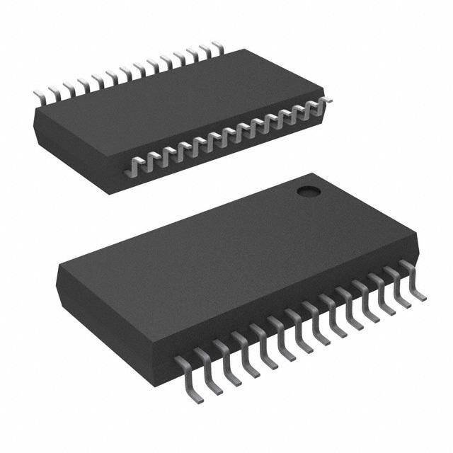
| 供应商器件封装 | 28-SSOP |
| 其它名称 | 296-29562-6 |
| 包装 | Digi-Reel® |
| 安装类型 | 表面贴装 |
| 封装/外壳 | 28-SSOP(0.209",5.30mm 宽) |
| 应用 | USB 音频 |
| 标准包装 | 1 |
| 类型 | DAC,USB |


- 商务部:美国ITC正式对集成电路等产品启动337调查
- 曝三星4nm工艺存在良率问题 高通将骁龙8 Gen1或转产台积电
- 太阳诱电将投资9.5亿元在常州建新厂生产MLCC 预计2023年完工
- 英特尔发布欧洲新工厂建设计划 深化IDM 2.0 战略
- 台积电先进制程称霸业界 有大客户加持明年业绩稳了
- 达到5530亿美元!SIA预计今年全球半导体销售额将创下新高
- 英特尔拟将自动驾驶子公司Mobileye上市 估值或超500亿美元
- 三星加码芯片和SET,合并消费电子和移动部门,撤换高东真等 CEO
- 三星电子宣布重大人事变动 还合并消费电子和移动部门
- 海关总署:前11个月进口集成电路产品价值2.52万亿元 增长14.8%


PDF Datasheet 数据手册内容提取
Product Sample & Technical Tools & Support & Folder Buy Documents Software Community PCM2704C,PCM2705C,PCM2706C,PCM2707C Burr-Brown Audio SBFS036B–MAY2015–REVISEDAUGUST2015 PCM270xC Stereo Audio DAC With USB Interface, Single-Ended Headphone Output and S/PDIF Output 1 Features 2 Applications • On-ChipUSBInterface: • USBHeadphones 1 – NoDedicatedDeviceDriverNeeded • USBAudioSpeaker – Full-SpeedTransceivers • USBCRT/LCDMonitor – FullyCompliantWithUSB2.0Specification • USBAudioInterfaceBox – USB1.1DescriptorsWithUSBAudioClass • USB-FeaturedConsumerAudioProduct Support 3 Description – CertifiedbyUSB-IF The PCM270xC are TI's single-chip USB stereo – PartiallyProgrammableDescriptors audio digital-to-analog converters (DACs) with USB – AdaptiveIsochronousTransferforPlayback 2.0 compliant full-speed protocol controller and – Bus-PoweredorSelf-PoweredOperation S/PDIF. The USB-protocol controller works with no software code, but USB descriptors can be modified • SamplingRates:32kHz,44.1kHz,and48kHz in some areas (for example, vendor ID/product ID) • On-ChipClockGeneratorWithSingle12-MHz through the use of an external ROM (PCM2704C and ClockSource PCM2706C) or serial peripheral interface (SPI) • SinglePowerSupply: (PCM2705C and PCM2707C). The PCM270xC also employ SpAct™ architecture, TI's unique system that – Bus-Powered:5V,Typical(V ) BUS recovers the audio clock from USB packet data. On- – Self-Powered:3.3V,Typical chip analog phase-locked loops (PLLs) with SpAct • 16-BitDelta-SigmaStereoDAC enableplaybackwithlowclockjitter. – AnalogPerformanceat5V(Bus-Powered), DeviceInformation(1) 3.3V(Self-Powered): PARTNUMBER PACKAGE BODYSIZE(NOM) – THD+N:0.006%R > 10kΩ,Self- L Powered PCM2704C SSOP(28) 5.30mm×10.20mm PCM2705C – THD+N:0.025%R =32 Ω L PCM2706C – SNR=98dB TQFP(32) 7.00mm×7.00mm PCM2707C – DynamicRange:98dB (1) For all available packages, see the orderable addendum at – P =12mW,R =32 Ω O L theendofthedatasheet. – OversamplingDigitalFilter BlockDiagram – PassbandRipple= ±0.04dB – Stop-BandAttenuation= –50dB USB – Single-EndedVoltageOutput HID Controls Line Out – AnalogLPFIncluded External ROM S/PDIF SPI PCM2704C/5C/6C/7C I2S • MultipleFunctions: – UptoEightHumanInterfaceDevice(HID) Interfaces(ModelandSettingDependent) PGND – SuspendFlag V DD AGNDR V – S/PDIFOutWithSCMS VCCL AGNDL CCR ZGND V – ExternalROMInterface(PCM2704C/6C) CCP DGND – SerialProgrammingInterface(PCM2705C/7C) – I2SInterface(SelectableonPCM2706C/7C) 1 An IMPORTANT NOTICE at the end of this data sheet addresses availability, warranty, changes, use in safety-critical applications, intellectualpropertymattersandotherimportantdisclaimers.PRODUCTIONDATA.
PCM2704C,PCM2705C,PCM2706C,PCM2707C SBFS036B–MAY2015–REVISEDAUGUST2015 www.ti.com Table of Contents 1 Features.................................................................. 1 9.1 Overview.................................................................18 2 Applications........................................................... 1 9.2 FunctionalBlockDiagrams.....................................18 3 Description............................................................. 1 9.3 FeatureDescription.................................................20 9.4 DeviceFunctionalModes........................................25 4 RevisionHistory..................................................... 2 9.5 Programming...........................................................26 5 DeviceComparisonTable..................................... 3 9.6 RegisterMaps.........................................................29 6 PinConfigurationandFunctions......................... 4 10 ApplicationandImplementation........................ 30 7 Specifications......................................................... 7 10.1 ApplicationInformation..........................................30 7.1 AbsoluteMaximumRatings......................................7 10.2 TypicalApplication ...............................................30 7.2 ESDRatings..............................................................7 11 PowerSupplyRecommendations..................... 37 7.3 RecommendedOperatingConditions......................8 12 Layout................................................................... 37 7.4 ThermalInformation:PCM2704C,PCM2705C.........8 12.1 LayoutGuidelines.................................................37 7.5 ThermalInformation:PCM2706C,PCM2707C.........8 12.2 LayoutExample....................................................37 7.6 ElectricalCharacteristics:PCM2704CDB, PCM2705CDB,PCM2706CPJT,PCM2707CPJT.....9 13 DeviceandDocumentationSupport................. 40 7.7 AudioInterfaceTimingCharacteristics...................11 13.1 DocumentationSupport........................................40 7.8 AudioClockTimingCharacteristics........................11 13.2 RelatedLinks........................................................40 7.9 ExternalROMReadInterfaceTiming 13.3 CommunityResources..........................................40 Characteristics.........................................................11 13.4 Trademarks...........................................................40 7.10 SPITimingCharacteristics....................................12 13.5 ElectrostaticDischargeCaution............................40 7.11 TypicalCharacteristics..........................................14 13.6 Glossary................................................................40 8 ParameterMeasurementInformation................17 14 Mechanical,Packaging,andOrderable 9 DetailedDescription............................................ 18 Information........................................................... 40 4 Revision History NOTE:Pagenumbersforpreviousrevisionsmaydifferfrompagenumbersinthecurrentversion. ChangesfromRevisionA(July2012)toRevisionB Page • AddedHandlingRatingstable,FeatureDescriptionsection,DeviceFunctionalModes,Applicationand Implementationsection,PowerSupplyRecommendationssection,Layoutsection,DeviceandDocumentation Supportsection,andMechanical,Packaging,andOrderableInformationsection ............................................................... 1 ChangesfromOriginal(August2011)toRevisionA Page • ChangedproductstatusfromMixedStatustoProductionData............................................................................................ 1 • ChangedFeaturessectiontoshowfullcompliancewithUSB2.0Specification(butstillusingUSB1.1descriptors)............ 1 • ChangedDescriptionsectiontoshowUSB2.0compliance(USB1.1wasabsorbedinto2.0specification).......................... 1 2 SubmitDocumentationFeedback Copyright©2015,TexasInstrumentsIncorporated ProductFolderLinks:PCM2704C PCM2705C PCM2706C PCM2707C
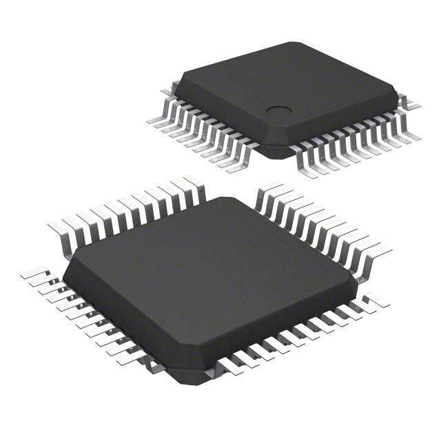
PCM2704C,PCM2705C,PCM2706C,PCM2707C www.ti.com SBFS036B–MAY2015–REVISEDAUGUST2015 5 Device Comparison Table FEATURE PCM2704C PCM2705C PCM2706C PCM2707C SupplyVoltage(V) 3.3,5 3.3,5 3.3,5 3.3,5 ControlInterface HID HID,SPI HID,SPI HID,SPI S/PDIFOutput S/PDIFOutput S/PDIFOutput S/PDIFOutput AdditionalFeatures HPOutput HPOutput HPOutput HPOutput Ext.ROMI/F Ext.ROMI/F PackageGroup SSOP SSOP TQFP TQFP Copyright©2015,TexasInstrumentsIncorporated SubmitDocumentationFeedback 3 ProductFolderLinks:PCM2704C PCM2705C PCM2706C PCM2707C
PCM2704C,PCM2705C,PCM2706C,PCM2707C SBFS036B–MAY2015–REVISEDAUGUST2015 www.ti.com 6 Pin Configuration and Functions PCM2704C,PCM2705CDBPackage 28-PinSSOP TopView XTO 1 28 XTI CK 2 27 SSPND DT 3 26 TEST0 PSEL 4 25 TEST1 DOUT 5 24 HID2/MD DGND 6 23 HID1/MC V 7 22 HID0/MS DD D- 8 21 HOST D+ 9 20 V CCP V 10 19 PGND BUS ZGND 11 18 V COM AGNDL 12 17 AGNDR V 13 16 V CCL CCR V L 14 15 V R OUT OUT PinFunctions:DBPackage(PCM2704C/PCM2705C) PIN DESCRIPTION NAME NO. I/O AGNDL 12 — AnaloggroundforheadphoneamplifierofL-channel AGNDR 17 — AnaloggroundforheadphoneamplifierofR-channel CK 2 O ClockoutputforexternalROM(PCM2704C).Mustbeleftopen(PCM2705C). D+ 9 I/O USBdifferentialinput/outputplus(1) D– 8 I/O USBdifferentialinput/outputminus(1) DGND 6 — Digitalground DOUT 5 O S/PDIFoutput DT 3 I/O Datainput/outputforexternalROM(PCM2704C).Mustbeleftopenwithpullupresistor(PCM2705C).(1) HID0/MS 22 I HIDkeystateinput(mute),activehigh(PCM2704C).MSinput(PCM2705C)(2) HID1/MC 23 I HIDkeystateinput(volumeup),activehigh(PCM2704C).MCinput(PCM2705C)(2) HID2/MD 24 I HIDkeystateinput(volumedown),activehigh(PCM2704C).MDinput(PCM2705C)(2) Hostdetectionduringself-poweredoperation(connecttoV ).Maxpowerselectduringbus-powered HOST 21 I operation(low:100mA,high:500mA).(3) BUS PGND 19 — AnaloggroundforDAC,OSC,andPLL PSEL 4 I Powersourceselect(low:self-power,high:bus-power)(1) SSPND 27 O Suspendflag,activelow(low:suspend,high:operational) TEST0 26 I Testpin.Mustbesethigh(1) TEST1 25 I Testpin.Mustbesethigh(1) V 10 — ConnecttoUSBpower(V )forbus-poweredoperation.ConnecttoV forself-poweredoperation. BUS BUS DD V 13 — AnalogpowersupplyforheadphoneamplifierofL-channel(4) CCL (1) LV-TTLlevel. (2) LV-TTLlevelwithinternalpulldown (3) LV-TTLlevel,5-Vtolerant (4) ConnectdecouplingcapacitortoGND.Supply3.3Vforself-poweredapplications. 4 SubmitDocumentationFeedback Copyright©2015,TexasInstrumentsIncorporated ProductFolderLinks:PCM2704C PCM2705C PCM2706C PCM2707C
PCM2704C,PCM2705C,PCM2706C,PCM2707C www.ti.com SBFS036B–MAY2015–REVISEDAUGUST2015 PinFunctions:DBPackage(PCM2704C/PCM2705C)(continued) PIN DESCRIPTION NAME NO. I/O V 20 — AnalogpowersupplyforDAC,OSC,andPLL(4) CCP V 16 — AnalogpowersupplyforheadphoneamplifierofR-channel(4) CCR V 18 — CommonvoltageforDAC(V /2).ConnectdecouplingcapacitortoPGND. COM CCP V 7 — Digitalpowersupply(4) DD V L 14 O DACanalogoutputforL-channel OUT V R 15 O DACanalogoutputforR-channel OUT XTI 28 I Crystaloscillatorinput(1) XTO 1 O Crystaloscillatoroutput ZGND 11 — Groundforinternalregulator Copyright©2015,TexasInstrumentsIncorporated SubmitDocumentationFeedback 5 ProductFolderLinks:PCM2704C PCM2705C PCM2706C PCM2707C
PCM2704C,PCM2705C,PCM2706C,PCM2707C SBFS036B–MAY2015–REVISEDAUGUST2015 www.ti.com PCM2706C,PCM2707CPJTPackage 32-PinTQFP TopView R L + COM GND CCR ROUT LOUT CCL GND GND V A V V V V A Z 32 31 30 29 28 27 26 25 PGND 1 24 VBUS VCCP 2 23 D+ HOST 3 22 D- FUNC3 4 21 V DD FUNC0 5 20 DGND HID0/MS 6 19 FUNC1 HID1/MC 7 18 FUNC2 HID2/MD 8 17 DOUT 9 10 11 12 13 14 15 16 SEL EST PND XTI XTO CK DT SEL F T S P S PinFunctions:PJTPackage(PCM2706C/PCM2707C) PIN DESCRIPTION NAME NO. I/O AGNDL 26 — AnaloggroundforheadphoneamplifierofL-channel AGNDR 31 — AnaloggroundforheadphoneamplifierofR-channel CK 14 O ClockoutputforexternalROM(PCM2706C).Mustbeleftopen(PCM2707C). D+ 23 I/O USBdifferentialinput/outputplus(1) D– 22 I/O USBdifferentialinput/outputminus(1) DGND 20 — Digitalground DOUT 17 O S/PDIFoutput/I2Sdataoutput DT 15 I/O Datainput/outputforexternalROM(PCM2706C).Mustbeleftopenwithpullupresistor(PCM2707C).(1) FSEL 9 I Functionselect(low:I2Sdataoutput,high:S/PDIFoutput)(2) FUNC0 5 I/O HIDkeystateinput(nexttrack),activehigh(FSEL=1).I2SLRclockoutput(FSEL=0).(3) FUNC1 19 I/O HIDkeystateinput(previoustrack),activehigh(FSEL=1).I2Sbitclockoutput(FSEL=0).(3) FUNC2 18 I/O HIDkeystateinput(stop),activehigh(FSEL=1).I2Ssystemclockoutput(FSEL=0).(3) FUNC3 4 I HIDkeystateinput(play/pause),activehigh(FSEL=1).I2Sdatainput(FSEL=0).(3) HID0/MS 6 I HIDkeystateinput(mute),activehigh(PCM2706C).MSinput(PCM2707C).(3) HID1/MC 7 I HIDkeystateinput(volumeup),activehigh(PCM2706C).MCinput(PCM2707C).(3) HID2/MD 8 I HIDkeystateinput(volumedown),activehigh(PCM2706C).MDinput(PCM2707C).(3) Hostdetectionduringself-poweredoperation(connecttoV ).Maxpowerselectduringbus-powered HOST 3 I operation.(low:100mA,high:500mA).(4) BUS PGND 1 — AnaloggroundforDAC,OSC,andPLL PSEL 16 I Powersourceselect(low:self-power,high:bus-power)(1) SSPND 11 O Suspendflag,activelow(low:suspend,high:operational) TEST 10 I Testpin.Mustbesethigh(1) (1) LV-TTLlevel (2) LV-TTLlevel. (3) LV-TTLlevelwithinternalpulldown (4) LV-TTLlevel,5-Vtolerant 6 SubmitDocumentationFeedback Copyright©2015,TexasInstrumentsIncorporated ProductFolderLinks:PCM2704C PCM2705C PCM2706C PCM2707C
PCM2704C,PCM2705C,PCM2706C,PCM2707C www.ti.com SBFS036B–MAY2015–REVISEDAUGUST2015 PinFunctions:PJTPackage(PCM2706C/PCM2707C)(continued) PIN DESCRIPTION NAME NO. I/O V 24 — ConnecttoUSBpower(V )forbus-poweredoperation.ConnecttoV forself-poweredoperation. BUS BUS DD V 27 — AnalogpowersupplyforheadphoneamplifierofL-channel(5) CCL V 2 — AnalogpowersupplyforDAC,OSC,andPLL(5) CCP V 30 — AnalogpowersupplyforheadphoneamplifierofR-channel(5) CCR V 32 — CommonvoltageforDAC(V /2).ConnectdecouplingcapacitortoPGND. COM CCP V 21 — Digitalpowersupply(5) DD V L 28 O DACanalogoutputforL-channel OUT V R 29 O DACanalogoutputforR-channel OUT XTI 12 I Crystaloscillatorinput(1) XTO 13 O Crystaloscillatoroutput ZGND 25 — Groundforinternalregulator (5) ConnectdecouplingcapacitortoGND.Supply3.3Vforself-poweredapplications. 7 Specifications 7.1 Absolute Maximum Ratings Overoperatingfree-airtemperaturerangeunlessotherwisenoted. (1) MIN MAX UNIT V –0.3 6.5 V BUS Supplyvoltage V ,V ,V ,V –0.3 4 V CCP CCL CCR DD Supplyvoltage V ,V ,V ,V ±0.1 V differences CCP CCL CCR DD Groundvoltage PGND,AGNDL,AGNDR,DGND,ZGND ±0.1 V differences HOST –0.3 6.5 V Digitalinputvoltage D+,D–,HID0/MS,HID1/MC,HID2/MD,XTI,XTO,DOUT, SSPND,CK,DT,PSEL,FSEL,TEST,TEST0,TEST1,FUNC0, –0.3 (V +0.3)<4 V DD FUNC1,FUNC2,FUNC3 V –0.3 (V +0.3)<4 V COM CCP Analoginputvoltage V R –0.3 (V +0.3)<4 V OUT CCR V L –0.3 (V +0.3)<4 V OUT CCL Inputcurrent(anypinsexceptsupplies) ±10 mA Ambienttemperatureunderbias –40 125 °C Junctiontemperature 150 °C Packagetemperature(IRreflow,peak) 260 °C Storagetemperature,T –55 150 °C stg (1) StressesbeyondthoselistedunderAbsoluteMaximumRatingsmaycausepermanentdamagetothedevice.Thesearestressratings only,andfunctionaloperationofthedeviceattheseoranyotherconditionsbeyondthoseindicatedunderRecommendedOperating Conditionsisnotimplied.Exposuretoabsolute-maximum-ratedconditionsforextendedperiodsmayaffectdevicereliability. 7.2 ESD Ratings MAX UNIT Electrostatic Humanbodymodel(HBM),perANSI/ESDA/JEDECJS-001,allpins(1) ±3000 V V (ESD) discharge Chargeddevicemodel(CDM),perJEDECspecificationJESD22-C101,allpins(2) ±1500 (1) JEDECdocumentJEP155statesthat500-VHBMallowssafemanufacturingwithastandardESDcontrolprocess. (2) JEDECdocumentJEP157statesthat250-VCDMallowssafemanufacturingwithastandardESDcontrolprocess. Copyright©2015,TexasInstrumentsIncorporated SubmitDocumentationFeedback 7 ProductFolderLinks:PCM2704C PCM2705C PCM2706C PCM2707C
PCM2704C,PCM2705C,PCM2706C,PCM2707C SBFS036B–MAY2015–REVISEDAUGUST2015 www.ti.com 7.3 Recommended Operating Conditions Overoperatingfree-airtemperaturerange. MIN NOM MAX UNIT V 4.35 5 5.25 BUS Supplyvoltage V V ,V ,V ,V 3 3.3 3.6 CCP CCL CCR DD Digitalinputlogiclevel TTL-compatible Digitalinputclockfrequency 11.994 12 12.006 MHz Analogoutputloadresistance 16 32 Ω Analogoutputloadcapacitance 100 pF Digitaloutputloadcapacitance 20 pF Operatingfree-airtemperature,T –25 85 °C A 7.4 Thermal Information: PCM2704C, PCM2705C PCM2704C,PCM2705C THERMALMETRIC(1) DB(SSOP) UNIT 28PINS R Junction-to-ambientthermalresistance 68.2 °C/W θJA R Junction-to-case(top)thermalresistance 27.2 °C/W θJC(top) R Junction-to-boardthermalresistance 29.5 °C/W θJB ψ Junction-to-topcharacterizationparameter 2.7 °C/W JT ψ Junction-to-boardcharacterizationparameter 29.1 °C/W JB (1) Formoreinformationabouttraditionalandnewthermalmetrics,seetheSemiconductorandICPackageThermalMetricsapplication report,SPRA953. 7.5 Thermal Information: PCM2706C, PCM2707C PCM2706C,PCM2707C THERMALMETRIC(1) PJT(TQFP) UNIT 32PINS R Junction-to-ambientthermalresistance 68.2 °C/W θJA R Junction-to-case(top)thermalresistance 27.2 °C/W θJC(top) R Junction-to-boardthermalresistance 29.5 °C/W θJB ψ Junction-to-topcharacterizationparameter 2.7 °C/W JT ψ Junction-to-boardcharacterizationparameter 29.1 °C/W JB (1) Formoreinformationabouttraditionalandnewthermalmetrics,seetheSemiconductorandICPackageThermalMetricsapplication report,SPRA953. 8 SubmitDocumentationFeedback Copyright©2015,TexasInstrumentsIncorporated ProductFolderLinks:PCM2704C PCM2705C PCM2706C PCM2707C
PCM2704C,PCM2705C,PCM2706C,PCM2707C www.ti.com SBFS036B–MAY2015–REVISEDAUGUST2015 7.6 Electrical Characteristics: PCM2704CDB, PCM2705CDB, PCM2706CPJT, PCM2707CPJT AllspecificationsatT =25°C,V =5V,ƒ =44.1kHz,ƒ =1kHz,and16-bitdata(unlessotherwisenoted).FortheHost A BUS S IN interface,applyUSBrevision1.1,full-speed.Foraudiodataformat,useUSBisochronousdataformat. PARAMETER TESTCONDITIONS MIN TYP MAX UNIT INPUTLOGIC Inputlogichighlevel 2 3.3 V V IH Inputlogichighlevel(1) 2 5.5 DC Inputlogiclowlevel –0.3 0.8 V V IL Inputlogiclowlevel(1) –0.3 0.8 DC Inputlogichighcurrent(2) V =3.3V ±10 IN I μA IH Inputlogichighcurrent V =3.3V 65 100 IN Inputlogiclowcurrent(2) V =0V ±10 IN I μA IL Inputlogiclowcurrent V =0V ±10 IN OUTPUTLOGIC Outputlogichighlevel(3) I =–2mA 2.8 OH V V OH DC Outputlogichighlevel I =–2mA 2.4 OH Outputlogiclowlevel(3) I =2mA 0.3 OL V V OL DC Outputlogiclowlevel I =2mA 0.4 OL CLOCKFREQUENCY Inputclockfrequency,XTI 11.994 12 12.006 MHz 32 ƒ Samplingfrequency 44.1 kHz S 48 DACCHARACTERISTICS Resolution 16 bits Audiodatachannel 1,2 channel DCACCURACY Gainmismatch,channel-to-channel ±2 ±8 %ofFSR Gainerror ±2 ±8 %ofFSR Bipolarzeroerror ±3 ±6 %ofFSR DYNAMICPERFORMANCE (4) R >10kΩ,self-powered, L 0.006% 0.01% V =0dB Line (5) OUT THD+ Totalharmonic R >10kΩ,bus-powered, L 0.012% 0.02% N distortion+noise V =0dB OUT R =32Ω,self-orbus- Headphone L 0.025% powered,V =0dB OUT THD+ Totalharmonicdistortion+noise V =–60dB 2% N OUT Dynamicrange EIAJ,A-weighted 90 98 dB SNR Signal-to-noiseratio EIAJ,A-weighted 90 98 dB Channelseparation 60 70 dB (1) HOSTpin. (2) D+,D–,HOST,TEST,TEST0,TEST1,DT,PSEL,FSEL,XTIpins. (3) FUNC0,FUNC1,andFUNC2pins. (4) ƒ =1kHz,usingtheSystemTwoCascade™audiomeasurementsystembyAudioPrecision®inRMSmodewitha20-kHzlow-pass IN filter(LPF)and400-Hzhigh-passfilter(HPF). (5) THD+Nperformancevariesslightly,dependingontheeffectiveoutputload,includingdummyloadR7andR8inFigure35. Copyright©2015,TexasInstrumentsIncorporated SubmitDocumentationFeedback 9 ProductFolderLinks:PCM2704C PCM2705C PCM2706C PCM2707C
PCM2704C,PCM2705C,PCM2706C,PCM2707C SBFS036B–MAY2015–REVISEDAUGUST2015 www.ti.com Electrical Characteristics: PCM2704CDB, PCM2705CDB, PCM2706CPJT, PCM2707CPJT (continued) AllspecificationsatT =25°C,V =5V,ƒ =44.1kHz,ƒ =1kHz,and16-bitdata(unlessotherwisenoted).FortheHost A BUS S IN interface,applyUSBrevision1.1,full-speed.Foraudiodataformat,useUSBisochronousdataformat. PARAMETER TESTCONDITIONS MIN TYP MAX UNIT ANALOGOUTPUT 0.55V Outputvoltage CCL V 0.55V PP CCR Centervoltage 0.5V V CCP Line AC-coupling 10 kΩ Loadimpedance Headphone AC-coupling 16 32 Ω –3dB 140 kHz LPFfrequencyresponse ƒ=20kHz –0.1 dB DIGITALFILTERPERFORMANCE Passband 0.454ƒ Hz S Stopband 0.546ƒ Hz S Passbandripple ±0.04 dB Stopbandattenuation –50 dB Delaytime 20/ƒ s S POWERSUPPLYREQUIREMENTS V Bus-powered 4.35 5 5.25 BUS Voltagerange V DC V ,V ,V ,V Self-powered 3 3.3 3.6 CCP CCL CCR DD Line DACoperation 23 30 mA Supplycurrent Headphone DACoperation(R =32Ω) 35 46 L Line/headphone Suspendmode (6) 150 190 μA Line DACoperation 76 108 Powerdissipation mW Headphone DACoperation(R =32Ω) 116 166 (self-powered) L Line/headphone Suspendmode (6) 495 684 μW Line DACoperation 115 158 Powerdissipation mW Headphone DACoperation(R =32Ω) 175 242 (bus-powered) L Line/headphone Suspendmode (6) 750 998 μW Internalpower- supplyvoltage (7) VCCP,VCCL,VCCR,VDD Bus-powered 3.2 3.35 3.5 VDC TEMPERATURERANGE Operatingtemperature –25 85 °C (6) InUSBsuspendedstate (7) V ,V ,V ,V pins.Thesepinsworkasoutputpinsofinternalpowersupplyforbus-poweredoperation. DD CCP CCL CCR 10 SubmitDocumentationFeedback Copyright©2015,TexasInstrumentsIncorporated ProductFolderLinks:PCM2704C PCM2705C PCM2706C PCM2707C
PCM2704C,PCM2705C,PCM2706C,PCM2707C www.ti.com SBFS036B–MAY2015–REVISEDAUGUST2015 7.7 Audio Interface Timing Characteristics LoadcapacitanceofLRCK,BCK,andDOUTis20pF.Fortimingdiagrams,seeFigure1andFigure2. MIN MAX UNIT t(BCY) BCKpulsecycletime 300 ns t(BCH) BCKpulseduration,high 100 ns t(BCL) BCKpulseduration,low 100 ns t(BL) LRCKdelaytimefromBCKfallingedge –20 40 ns t(BD) DOUTdelaytimefromBCKfallingedge –20 40 ns t(LD) DOUTdelaytimefromLRCKedge –20 40 ns t(DS) DINsetuptime 20 ns t(DH) DINholdtime 20 ns 7.8 Audio Clock Timing Characteristics Loadcapacitanceis20pF.Fortimingdiagrams,seeFigure3. MIN MAX UNIT t(SLL),t(SLH) LRCKdelaytimefromSYSCKrisingedge –5 10 ns t(SBL),t(SBH) BCKdelaytimefromSYSCKrisingedge –5 10 ns 7.9 External ROM Read Interface Timing Characteristics Fortimingdiagrams,seeFigure4. MIN MAX UNIT ƒ CKclockfrequency 100 kHz (CK) t BusfreetimebetweenaSTOPandaSTARTcondition 4.7 μs (BUF) t LowperiodoftheCKclock 4.7 μs (LOW) t HighperiodoftheCKclock 4 μs (HI) t SetuptimeforSTART/repeatedSTARTcondition 4.7 μs (RS-SU) t (S-HD) HoldtimeforSTART/repeatedSTARTcondition 4 μs t (RS-HD) t Datasetuptime 250 ns (D-SU) t Dataholdtime 0 900 ns (D-HD) t RisetimeofCKsignal 20+0.1C 1000 ns (CK-R) B t FalltimeofCKsignal 20+0.1C 1000 ns (CK-F) B t RisetimeofDTsignal 20+0.1C 1000 ns (DT-R) B t FalltimeofDTsignal 20+0.1C 1000 ns (DT-F) B t SetuptimeforSTOPcondition 4 μs (P-SU) C CapacitiveloadforDTandCKlines 400 pF B V Noisemarginathighlevelforeachconnecteddevice(includinghysteresis) 0.2V V NH DD Copyright©2015,TexasInstrumentsIncorporated SubmitDocumentationFeedback 11 ProductFolderLinks:PCM2704C PCM2705C PCM2706C PCM2707C
PCM2704C,PCM2705C,PCM2706C,PCM2707C SBFS036B–MAY2015–REVISEDAUGUST2015 www.ti.com 7.10 SPI Timing Characteristics Fortimingdiagrams,seeFigure5. MIN MAX UNIT t(MCY) MCpulsecycletime 100 ns t(MCL) MClow-leveltime 50 ns t(MCH) MChigh-leveltime 50 ns t(MHH) MShigh-leveltime 100 ns t(MLS) MSfallingedgetoMCrisingedge 20 ns t(MLH) MSholdtime 20 ns t(MDH) MDholdtime 15 ns t(MDS) MDsetuptime 20 ns SYSCK (256 f ) S 1/f S LRCK L-Channel R-Channel BCK (64 f ) S DOUT 1 2 3 14 15 16 1 2 3 14 15 16 1 2 MSB LSB MSB LSB MSB DIN 1 2 3 14 15 16 1 2 3 14 15 16 1 2 Figure1. AudioDataInterfaceFormat LRCK (Output) 50% of VDD t (BCH) t(BCL) t(BL) BCK (Output) 50% of VDD t (BCY) t(BD) t(LD) DOUT (Output) 50% of VDD t (DS) t (DH) DIN (Input) 50% of VDD Figure2. AudioInterfaceTiming 12 SubmitDocumentationFeedback Copyright©2015,TexasInstrumentsIncorporated ProductFolderLinks:PCM2704C PCM2705C PCM2706C PCM2707C
PCM2704C,PCM2705C,PCM2706C,PCM2707C www.ti.com SBFS036B–MAY2015–REVISEDAUGUST2015 SYSCK (Output) t t (SLL) (SLH) LRCK (Output) t(SBL) t(SBH) BCK (Output) Figure3. AudioClockTiming Repeated Start Start Stop t t (D-HD) (DT-F) t(BUF) t(D-SU) t(DT-R) t(P-SU) DT t t (CK-R) (RS-HD) t (LOW) CK t(S-HD) t(HI) t(RS-SU) t (CK-F) Figure4. ExternalROMReadInterfaceTimingRequirements t (MHH) MS 50% of VDD t(MLS) t(MCL) t(MCH) t(MLH) MC 50% of VDD t (MCY) LSB MD 50% of VDD t (MDS) t (MDH) Figure5. SPITimingDiagram Copyright©2015,TexasInstrumentsIncorporated SubmitDocumentationFeedback 13 ProductFolderLinks:PCM2704C PCM2705C PCM2706C PCM2707C
PCM2704C,PCM2705C,PCM2706C,PCM2707C SBFS036B–MAY2015–REVISEDAUGUST2015 www.ti.com 7.11 Typical Characteristics 7.11.1 InternalFilter:DACDigitalInterpolationFilterFrequencyResponse AllspecificationsatT =25°C,V =5V,ƒ =44.1kHz,ƒ =1kHz,16-bitdata(unlessotherwisenoted). A BUS S IN 0 0.05 0.04 -20 0.03 -40 0.02 B) B) mplitude (d --6800 mplitude (d -00..00110 A -100 A -0.02 -0.03 -120 -0.04 -140 -0.05 0 1 2 3 4 0 0.1 0.2 0.3 0.4 0.5 Frequency (× fS) G001 Frequency (× fS) G002 Figure6.FrequencyResponse Figure7.PassbandRipple 7.11.2 InternalFilter:DACAnalogLow-PassFilterFrequencyResponse AllspecificationsatT =25°C,V =5V,ƒ =44.1kHz,ƒ =1kHz,16-bitdata(unlessotherwisenoted). A BUS S IN 0 0 -0.5 -20 B) B) d d ude ( -1 ude ( -40 plit plit m m A A -1.5 -60 -2 -80 0.01 0.1 1 10 100 1 10 100 1k 10k Frequency (kHz) Frequency (kHz) G003 G004 Figure8.PassbandCharacteristics Figure9.StopBandCharacteristics 7.11.3 GeneralCharacteristics AllspecificationsatT =25°C,V =5V,ƒ =44.1kHz,ƒ =1kHz,16-bitdata(unlessotherwisenoted). A BUS S IN 0.05 0.05 %) %) oise ( 0.04 oise ( 0.04 N N + + n n Distortio 0.03 32Ω Distortio 0.03 32Ω nic 0.02 nic 0.02 mo 10 kΩ mo otal Har 0.01 otal Har 0.01 10 kΩ T T 0 0 –50 –25 0 25 50 75 100 –50 –25 0 25 50 75 100 Free-Air Temperature (°C) Free-Air Temperature (°C) G005 G006 Figure10.TotalHarmonicDistortion+NoisevsFree-Air Figure11.TotalHarmonicDistortion+NoisevsFree-Air Temperature Temperature 14 SubmitDocumentationFeedback Copyright©2015,TexasInstrumentsIncorporated ProductFolderLinks:PCM2704C PCM2705C PCM2706C PCM2707C
PCM2704C,PCM2705C,PCM2706C,PCM2707C www.ti.com SBFS036B–MAY2015–REVISEDAUGUST2015 General Characteristics (continued) AllspecificationsatT =25°C,V =5V,ƒ =44.1kHz,ƒ =1kHz,16-bitdata(unlessotherwisenoted). A BUS S IN 0.05 0.05 %) %) e ( e ( ois 0.04 ois 0.04 N N + + n n ortio 0.03 32Ω ortio 0.03 32Ω Dist Dist nic 0.02 nic 0.02 mo 10 kΩ mo al Har 0.01 al Har 0.01 10 kΩ ot ot T T 0 0 4 4.5 5 5.5 3 3.1 3.2 3.3 3.4 3.5 3.6 Supply Voltage (V) Supply Voltage (V) G007 G008 Figure12.TotalHarmonicDistortion+NoisevsSupply Figure13.TotalHarmonicDistortion+NoisevsSupply Voltage Voltage 0.05 0.05 %) %) e ( e ( ois 0.04 ois 0.04 N N + + n 32Ω n ortio 0.03 ortio 0.03 32Ω Dist Dist c 0.02 c 0.02 ni ni mo 10 kΩ mo al Har 0.01 al Har 0.01 10 kΩ ot ot T T 0 0 30 35 40 45 50 30 35 40 45 50 Sampling Frequency (kHz) Sampling Frequency (kHz) G009 G010 Figure14.TotalHarmonicDistortion+NoisevsSampling Figure15.TotalHarmonicDistortion+NoisevsSampling Frequency Frequency 105 105 dB) 103 dB) 103 R ( R ( N N S S d 101 d 101 n n a a e e g g n n Ra 99 Ra 99 c Dynamic Range c Dynamic Range mi mi a a yn 97 yn 97 D D SNR SNR 95 95 –50 –25 0 25 50 75 100 –50 –25 0 25 50 75 100 Free-Air Temperature (°C) Free-Air Temperature (°C) G011 G012 Figure16.DynamicRangeandSNRvsFree-Air Figure17.DynamicRangeandSNRvsFree-Air Temperature Temperature Copyright©2015,TexasInstrumentsIncorporated SubmitDocumentationFeedback 15 ProductFolderLinks:PCM2704C PCM2705C PCM2706C PCM2707C
PCM2704C,PCM2705C,PCM2706C,PCM2707C SBFS036B–MAY2015–REVISEDAUGUST2015 www.ti.com General Characteristics (continued) AllspecificationsatT =25°C,V =5V,ƒ =44.1kHz,ƒ =1kHz,16-bitdata(unlessotherwisenoted). A BUS S IN 105 105 dB) 103 dB) 103 R ( R ( N N S S d 101 d 101 n n a a e e g g Ran 99 Dynamic Range Ran 99 Dynamic Range c c mi mi a a yn 97 yn 97 D SNR D SNR 95 95 4 4.5 5 5.5 3 3.1 3.2 3.3 3.4 3.5 3.6 Supply Voltage (V) Supply Voltage (V) G013 G014 Figure18.DynamicRangeandSNRvsSupplyVoltage Figure19.DynamicRangeandSNRvsSupplyVoltage 105 105 dB) 103 dB) 103 R ( R ( N N S S Dynamic Range d 101 d 101 n n e a Dynamic Range e a g g n n Ra 99 Ra 99 c c mi mi a a yn 97 yn 97 D SNR D SNR 95 95 30 35 40 45 50 30 35 40 45 50 Sampling Frequency (kHz) Sampling Frequency (kHz) G015 G016 Figure20.DynamicRangeandSNRvsSampling Figure21.DynamicRangeandSNRvsSampling Frequency Frequency 200 200 A) 150 A) 150 m m nt ( nt ( e e Curr 100 Curr 100 d d n n e e p p Sus 50 Sus 50 0 0 4 4.5 5 5.5 -40 -20 0 20 40 60 80 100 Supply Voltage (V) Free-Air Temperature (°C) G017 G018 Figure22.SuspendCurrentvsSupplyVoltage Figure23.SuspendCurrentvsFree-AirTemperature 16 SubmitDocumentationFeedback Copyright©2015,TexasInstrumentsIncorporated ProductFolderLinks:PCM2704C PCM2705C PCM2706C PCM2707C
PCM2704C,PCM2705C,PCM2706C,PCM2707C www.ti.com SBFS036B–MAY2015–REVISEDAUGUST2015 General Characteristics (continued) AllspecificationsatT =25°C,V =5V,ƒ =44.1kHz,ƒ =1kHz,16-bitdata(unlessotherwisenoted). A BUS S IN 0 0 -20 -20 -40 -40 B) B) e (d -60 e (d -60 d d u u plit -80 plit -80 m m A A -100 -100 -120 -120 -140 -140 0 5 10 15 20 0 20 40 60 80 100 120 Frequency (kHz) Frequency (kHz) G019 G020 Figure24.OutputSpectrum(–60dB,N=8192) Figure25.OutputSpectrum(–60dB,N=8192) 8 Parameter Measurement Information AllparametersaremeasuredaccordingtotheconditionsdescribedinSpecifications. Copyright©2015,TexasInstrumentsIncorporated SubmitDocumentationFeedback 17 ProductFolderLinks:PCM2704C PCM2705C PCM2706C PCM2707C
PCM2704C,PCM2705C,PCM2706C,PCM2707C SBFS036B–MAY2015–REVISEDAUGUST2015 www.ti.com 9 Detailed Description 9.1 Overview The PCM2704C/5C/6C/7C is a stereo audio digital-to-analog converter (DAC) with USB connection capability andaS/PDIFdigitalinterface. The PCM2704C/5C/6C/7C can be used in self-powered and bus-powered modes. These devices meet the requirements of USB2.0 standard connection. The PCM2704C/5C/6C/7C has digital input from the USB port. The PCM2704C/5C provides two different paths for the audio data, one of which goes to the digital S/PDIF output, and the other to the analog output through the DAC. The PCM2706C/7C provides three different paths for the audio data; to the digital S/PDIF output, to the analog output through the DAC, and leading the audio data totheI2Sdigitaloutput(theI2SpathisselectabletroughFSELpin9). The PCM2704C has 3 external interrupts (HID) which control the Mute, Volume Up, and Volume Down; these control inputs are active High. The PCM2706C has 7 external interrupts (I2S/HID control is selectable trough FSEL pin 9) which control the Mute, Volume Up, Volume Down, Next track, Previous track, Play/Pause, and Stop; these control inputs are active High. The PCM2704C/5C/6C/7C requires a 12-MHz clock, which can be providedbyanexternalclockorgeneratedbyabuilt-incrystalresonator. 9.2 Functional Block Diagrams VCCP VCCL VCCR VDD PGND AGNDL AGNDR DGND ZGND Power Manager SSPND 5-V to 3.3-V Voltage Regulator VBUS VCOM USB Protocol VOUTL AnPaLlLog Controller DAC VOUTR ECnodnptoroinlt USB SIE XCVR DD+- DOUT S/PDIF Encoder EEPROM CK FIFO ISO-Out Interface(1) DT Buffer Endpoint HOST HID0/MS HID Serial Peripheral PSEL Endpoint Interface(2) HID1/MC HID2/MD TEST0 TEST1 96 MHz Tracker PLL (x 8) (SpAct) XTI 12 MHz XTO (1) AppliestoPCM2704CDB (2) AppliestoPCM2705CDB Figure26. PCM2704C/PCM2705C 18 SubmitDocumentationFeedback Copyright©2015,TexasInstrumentsIncorporated ProductFolderLinks:PCM2704C PCM2705C PCM2706C PCM2707C
PCM2704C,PCM2705C,PCM2706C,PCM2707C www.ti.com SBFS036B–MAY2015–REVISEDAUGUST2015 Functional Block Diagrams (continued) V V V V PGND AGNDL AGNDR DGND ZGND CCP CCL CCR DD Power Manager SSPND 5-V to 3.3-V Voltage Regulator V BUS VCOM USB Protocol V L Analog Controller OUT PLL DAC VOUTR ECnodnptoroinlt B SIE CVR D+ US X D- S/PDIF DOUT Encoder DOUT FSEL LRCK FUNC0 BCK 2 FUNC1 IS EEPROM CK SYSCK Interface (1) FUNC2 FIFO ISO-Out Interface DT FUNC3 DIN Buffer Endpoint HOST (1) HID3: Next Track (1) HID4: Previous Track (1) HID0/MS HID5: Stop HID Serial Peripheral HID6: Play/Pause(1) Endpoint Interface(2) HHIIDD12//MMCD PSEL TEST 96 MHz Tracker PLL (x 8) (SpAct) XTI 12 MHz XTO (1) AppliestoPCM2706CPJT (2) AppliestoPCM2707CPJT Figure27. PCM2706C/PCM2707C Copyright©2015,TexasInstrumentsIncorporated SubmitDocumentationFeedback 19 ProductFolderLinks:PCM2704C PCM2705C PCM2706C PCM2707C
PCM2704C,PCM2705C,PCM2706C,PCM2707C SBFS036B–MAY2015–REVISEDAUGUST2015 www.ti.com 9.3 Feature Description 9.3.1 ClockandReset For both USB and audio functions, the PCM2704C/5C/6C/7C require a 12-MHz (±500 ppm) clock that can be generated by the onboard oscillator using a 12-MHz crystal resonator. The 12-MHz crystal resonator must be connectedtotheXTIpin(pin28forthePCM2704C/5C,pin12forthePCM2706C/7C)andtheXTOpin(pin1for the PCM2704C/5C, pin 13 for the PCM2706C/7C) with one large (1-MΩ) resistor and two small capacitors; the capacitance of these components depends on the specified load capacitance of the crystal resonator. An external clock can be supplied from XTI (pin 28 for the PCM2704C/5C, pin 12 for the PCM2706C/7C). If an external clock is supplied, XTO (pin 1 for the PCM2704C/5C, pin 13 for the PCM2706C/7C) must be left open. No clock disabling pin is provided; therefore, TI does not recommend to use the external clock supply. SSPND (pin27forthePCM2704C/5C,pin11forthePCM2706C/7C)cannotuseclockdisabling. ThePCM2704C/5C/6C/7Chaveaninternalpower-onresetcircuit,whichworksautomaticallywhenV (pin7for DD the PCM2704C/5C, pin 21 for the PCM2706C/7C) exceeds 2-V typical (1.6 to 2.4 V), which is equivalent to V BUS (pin10forthePCM2704C/5C,pin24forthePCM2706C/7C)exceeding3-Vtypicalforbus-poweredapplications. Approximately700μsisrequireduntilaninternalresetreleaseoccurs. 9.3.2 OperationModeSelection ThePCM2704C/5C/6C/7Chavethefollowingmode-selectpins. 9.3.2.1 PowerConfigurationSelect/HostDetection PSEL (pin 4 for the PCM2704C/5C, pin 16 for the PCM2706C/7C) is dedicated to selecting the power source. This selection affects the configuration descriptor. While in bus-powered operation, the maximum power consumption from V is determined by the HOST pin (pin 21 for the PCM2704C/5C, pin 3 for the BUS PCM2706C/7C). For self-powered operation, the HOST pin must be connected to V of the USB bus with a BUS pulldown resistor to detect attach and detach. (To avoid excessive suspend current, the pulldown should be a high-valueresistor.)Table1summarizesthepowerconfigurationselectoptions. Table1.PowerConfigurationSelect PSEL DESCRIPTION 0 Self-powered 1 Bus-powered HOST DESCRIPTION 0 DetachedfromUSB(self-powered)/100mA(bus-powered) 1 AttachedtoUSB(self-powered)/500mA(bus-powered) 9.3.2.2 FunctionSelect(PCM2706C/7COnly) FSEL (pin 9) determines the function of the FUNC0 through FUNC3 pins (pins 4, 5, 18, and 19) and DOUT (pin 17). When the I2S interface is required, FSEL must be low. Otherwise, FSEL must be high. Table 2 lists the functionalityoftheFUNC0throughFUNC3pins,basedontheFSELpin. Table2.FunctionSelect FSEL DOUT FUNC0 FUNC1 FUNC2 FUNC3 0 Dataout(I2S) LRCK(I2S) BCK(I2S) SYSCK(I2S) Datain(I2S) 1 S/PDIFdata Nexttrack(HID) (1) Previoustrack(HID) (1) Stop(HID) (1) Play/pause(HID) (1) (1) ValidonthePCM2706Conly;nofunctionassignedonthePCM2707C. 9.3.3 DAC The PCM2704C/5C/6C/7C have a DAC that uses an oversampling technique with 128-ƒ , second-order, multi-bit S noise shaping. This technique provides extremely-low quantization noise in the audio band, and the built-in analog low-pass filter removes the high-frequency components of the noise-shaping signal. The DAC analog outputs,V LandV R,aresentthroughtheheadphoneamplifierandcanprovide12mWat32Ω aswellas OUT OUT 1.8V intoa10-kΩ load. PP 20 SubmitDocumentationFeedback Copyright©2015,TexasInstrumentsIncorporated ProductFolderLinks:PCM2704C PCM2705C PCM2706C PCM2707C
PCM2704C,PCM2705C,PCM2706C,PCM2707C www.ti.com SBFS036B–MAY2015–REVISEDAUGUST2015 9.3.4 DigitalAudioInterface:S/PDIFOutput The PCM2704C/5C/6C/7C employ S/PDIF output. Isochronous-out data from the host are encoded to S/PDIF output DOUT, as well as to DAC analog outputs V L and V R. The interface format and timing follow the OUT OUT IEC-60958 standard. Monaural data are converted to the stereo format at the same data rate. S/PDIF output is notsupportedintheI2SI/Fenablemode.Theimplementationofthisfeatureisoptional. NOTE It is the responsibility of the user to determine whether or not to implement this feature in theendapplication. 9.3.4.1 ChannelStatusInformation Channel status information is fixed, and includes consumer application, PCM mode, copyright, and digital/digital converter data. All other bits are fixed as 0s, except for the sample frequency, which is set automatically accordingtothedatareceivedthroughtheUSB. 9.3.4.2 CopyrightManagement Digital audio data output is always encoded as original with SCMS control. Only one generation of digital duplicationisallowed. 9.3.5 DigitalAudioInterface:I2SInterfaceOutput(PCM2706C/7C) The PCM2706C and PCM2707C can support the I2S interface, which is enabled by the FSEL pin (pin 9). In the I2S interface-enabled mode, pins 4, 18, 19, 5, and 17 are assigned as DIN, SYSCK, BCK, LRCK, and DOUT, respectively. These pins provide digital output/input data in the 16-bit I2S format, which is also accepted by the internal DAC. Figure 1, Figure 2, and Figure 3 show the I2S interface format and timing. Audio Interface Timing Characteristics and Audio Clock Timing Characteristics list the audio interface timing and audio clock timing characteristics,respectively. 9.3.6 DescriptorDataModification The descriptor data can be modified through the I2C port by external ROM (PCM2704C/6C) or through the SPI port by an SPI host such as an MCU (PCM2705C/7C) under a particular configuration of the PSEL and HOST pins. Setting both the PSEL and the HOST pins high is necessary to modify the descriptor data; the D+ pin pullup resistor must not be activated before programming the descriptor data through the external ROM or SPI port is completed. The descriptor data must be sent from an external ROM to the PCM2704C/6C or from the SPI host to the PCM2705C/7C in LSB first format, with a specified byte order. Additionally, the power attribute and max power contents must be consistent with the PSEL setting and the power usage from the USB V of the BUS endapplication.Therefore,thedevicedoesnotsupportdescriptordatamodificationinself-poweredconfiguration (PSEL=low). 9.3.7 ExternalROMDescriptor(PCM2704C/6C) The PCM2704C/6C support an external ROM interface to override internal descriptors. Pin 3 (for the PCM2704C) or pin 15 (for the PCM2706C) is assigned as DT (serial data), and pin 2 (for the PCM2704C) or pin 14 (for the PCM2706C) is assigned as CK (serial clock) of the I2C interface when using the external ROM descriptor. Descriptor data are transferred from the external ROM to the PCM2704C/6C through the I2C interface the first time when the device is activated after a power-on reset. Before completing a read of the external ROM, the PCM2704C/6C reply with NACK for any USB command request from the host to the device itself. The descriptordata,whichcanbeintheexternalROM,mustmeettheseparameters: • StringdescriptorsmustbedescribedinANSIASCIIcode(1byteforeachcharacter). • Stringdescriptorsareconvertedautomaticallytounicodestringsfortransmissiontothehost. • ThedeviceaddressoftheexternalROMisfixedas0xA0. The data bits must be sent from LSB to MSB on the I2C bus. This condition means that each byte of data must be stored with its bits in reverse order. A read operation is performed at a frequency of XTI/384 (approximately 30 kHz). The power attribute and max power contents must be consistent with the end application circuit configuration (the PSEL setting and the actual power usage from V of the USB connector); otherwise, it may BUS causeimproperorunexpectedPCM2704C/6Coperation. Copyright©2015,TexasInstrumentsIncorporated SubmitDocumentationFeedback 21 ProductFolderLinks:PCM2704C PCM2705C PCM2706C PCM2707C
PCM2704C,PCM2705C,PCM2706C,PCM2707C SBFS036B–MAY2015–REVISEDAUGUST2015 www.ti.com Thedatamustbestoredfromaddress0x00andmustconsistof57bytes,accordingtotheselistedparameters: • VendorID(2bytes) • ProductID(2bytes) • Productstring(16bytesinANSIASCIIcode) • Vendorstring(32bytesinANSIASCIIcode) • Powerattribute(1byte) • Maxpower(1byte) • AuxiliaryHIDusageIDinreportdescriptor(3bytes) Figure28showsthetimingforanexternalROMreadoperation.Table3 summarizesthetimingcharacteristics. DT CK 1-7 8 9 1-8 9 1-8 9 9 S P Device Address R/W ACK DATA ACK DATA ACK NACK Start R/W: Read operation if‘1’; otherwise, Write operation Stop Condition ACK: Acknowledgement of a byte if‘0’ Condition DATA: 8 bits (1 byte) NACK: No acknowledgement if‘1’ Figure28. ExternalROMReadOperation Table3.ExternalROMReadOperationCharacteristics M M M S S M S M S M M S Deviceaddress R/W ACK DATA ACK DATA ACK ... NACK P 22 SubmitDocumentationFeedback Copyright©2015,TexasInstrumentsIncorporated ProductFolderLinks:PCM2704C PCM2705C PCM2706C PCM2707C
PCM2704C,PCM2705C,PCM2706C,PCM2707C www.ti.com SBFS036B–MAY2015–REVISEDAUGUST2015 9.3.8 ExternalROMExample ExternalROMdata(sampleset) 0xBB, 0x08, 0x04, 0x27, 0x50, 0x72, 0x6F, 0x64, 0x75, 0x63, 0x74, 0x20, 0x73, 0x74, 0x72, 0x69, 0x6E, 0x67, 0x73, 0x2E, 0x56, 0x65, 0x6E, 0x64, 0x6F, 0x72, 0x20, 0x73, 0x74, 0x72, 0x69, 0x6E, 0x67, 0x73, 0x20, 0x61, 0x72, 0x65, 0x20, 0x70, 0x6C, 0x61, 0x63, 0x65, 0x64, 0x20, 0x68, 0x65, 0x72, 0x65, 0x2E, 0x20, 0x80, 0x7D, 0x0A, 0x93, 0x01 Explanation Dataarestoredbeginningataddress0x00 VendorID:0x08BB ProductID: 0x2704 Productstring:Productstrings(16bytes) Vendorstring: Vendorstringsareplacedhere(32bytes,31visiblecharactersarefollowedby1space). Powerattribute(bmAttribute): 0x80(bus-powered) Maxpower(maxPower): 0x7D(250mA) AuxiliaryHIDusageID:0x0A,0x93,0x01(ALA/Vcapture) Note that the data bits must be sent from LSB to MSB on the I2C bus. Therefore, each data byte must be stored withitsbitsinreverseorder. 9.3.9 SerialProgrammingInterface(PCM2705C/7C) The PCM2705C/7C supports a SPI to program the descriptor and to set the HID state. External ROM Descriptor (PCM2704C/6C) describes descriptor data. Figure 5 shows the SPI timing; SPI Timing Characteristics lists the respectivetimingcharacteristics. Figure29showstheSPIwritetimingsequence. (1) Single Write Operation 16 Bits MS MC MD MSB LSB MSB (2) Continuous Write Operation 16 Bits?NFrames MS MC MD MSB LSB MSB NFrames LSB MSB LSB Figure29. SPIWriteOperation Copyright©2015,TexasInstrumentsIncorporated SubmitDocumentationFeedback 23 ProductFolderLinks:PCM2704C PCM2705C PCM2706C PCM2707C
PCM2704C,PCM2705C,PCM2706C,PCM2707C SBFS036B–MAY2015–REVISEDAUGUST2015 www.ti.com 9.3.10 USBHostInterfaceSequence 9.3.10.1 Power-On,Attach,andPlaybackSequence The PCM2704C/5C/6C/7C are ready for setup when the reset sequence has finished and the USB bus is attached. After a connection has been established (through the setup process), the PCM2704C/5C/6C/7C are ready to accept USB audio data. While waiting for the audio data (that is, the device is in an idle state), the analogoutputissettobipolarzero(BPZ). Upon receiving the audio data, the PCM2704C/5C/6C/7C stores the first audio packet in the internal storage buffer. The packet contains 1 ms of audio data. The PCM2704C/5C/6C/7C start playing the audio data after detecting the next subsequent start-of-frame (SOF) packet. Figure 30 shows the initial operation sequence for thedevice. 3.3 V (typ) V 2.0 V (typ) DD 0 V Bus Reset Set Configuration First Audio Data Second Audio Data Bus Idle D+ / D- SOF SOF SOF SSPND BPZ V L OUT V R OUT Device Setup 1 ms 700ms Internal Reset Ready for Setup Ready for Playback Figure30. InitialSequence 9.3.10.2 Play,Stop,andDetachSequence Whenthehostfinishesorabortsplayback,thePCM2704C/5C/6C/7Cstopplayingafterthelastaudiodataoutput iscomplete.Figure31showstheplay,stop,anddetachsequence. 24 SubmitDocumentationFeedback Copyright©2015,TexasInstrumentsIncorporated ProductFolderLinks:PCM2704C PCM2705C PCM2706C PCM2707C
PCM2704C,PCM2705C,PCM2706C,PCM2707C www.ti.com SBFS036B–MAY2015–REVISEDAUGUST2015 V BUS Audio Data Audio Data Last Audio Data D+ / D- SOF SOF SOF SOF SOF V L OUT V R OUT 1 ms Detach Figure31. Play,Stop,andDetachSequence 9.3.10.3 SuspendandResumeSequence The PCM2704C/5C/6C/7C enter a suspended state after the USB bus has been in a constant idle state for approximately 5 ms. While the PCM2704C/5C/6C/7C are in this suspended state, the SSPND flag (pin 27 for the PCM2704C/5C, pin 11 for the PCM2706C/7C) is asserted. The PCM2704C/5C/6C/7C wake up immediately when detecting a non-idle state on the USB bus. Figure 32 shows the operating sequence for the suspend and resumeprocess. Idle D+ / D- SSPND 5 ms Suspend V L OUT V R OUT Active 2.5 ms Active Figure32. SuspendandResume 9.3.11 OperatingEnvironment For current information on the PCM2704C/2705C/2706C/2707C operating environments, see the Updated Operating Environments for PCM270X, PCM290X Applications application report, SLAA374, available through theTIwebsiteatwww.ti.com. 9.4 Device Functional Modes The PCM2903C is a USB-controlled device. The PCM2903C is a digital-to-analog converter (DAC), with digital input (that goes to a D/A converter) and analog output, alongside the digital path to USB and S/PDIF and I2S (onlyinPCM2706C/7C).AwiderexplanationoftheseoperationalmodesisshowninFeatureDescription. Copyright©2015,TexasInstrumentsIncorporated SubmitDocumentationFeedback 25 ProductFolderLinks:PCM2704C PCM2705C PCM2706C PCM2707C
PCM2704C,PCM2705C,PCM2706C,PCM2707C SBFS036B–MAY2015–REVISEDAUGUST2015 www.ti.com 9.5 Programming 9.5.1 USBInterface Control data and audio data are transferred to the PCM2704C/5C/6C/7C through the D+ pin (pin 9 for the PCM2704C/5C, pin 23 for the PCM2706C/7C) and D– pin (pin 8 for the PCM2704C/5C, pin 22 for the PCM2706C/7C). D+ should be pulled up with a 1.5-kΩ (±5%) resistor. To avoid back voltage in self-powered operation,thedevicemustnotprovidepowertothepullupresistoronD+whileV oftheUSBportisinactive. BUS All data to/from the PCM2704C/5C/6C/7C are transferred at full speed. Table 4 shows the information that is provided in the device descriptor. Some parts of the device descriptor can be modified through external ROM (PCM2704C/6C)orSPI(PCM2705C/7C). Table4.DeviceDescriptor DEVICEDESCRIPTOR DESCRIPTION USBrevision 1.1compliant Deviceclass 0x00(devicedefinedinterfacelevel) Devicesubclass 0x00(notspecified) Deviceprotocol 0x00(notspecified) Maxpacketsizeforendpoint0 8bytes VendorID 0x08BB(defaultvalue,canbemodified) 0x27C4/0x27C5/0x27C6/0x27C7(Thesevaluescorrespondtothemodelnumber,andthevaluecan ProductID bemodified.) Devicereleasenumber 1.0(0x0100) Numberofconfigurations 1 Vendorstrings BurrBrownfromTexasInstruments(defaultvalue,canbemodified) Productstrings USBAUDIO DAC(defaultvalue,canbemodified) Serialnumber Notsupported Table 5 shows the information contained in the configuration descriptor. Some parts of the configuration descriptorcanbemodifiedthroughexternalROM(PCM2704C/6C)orSPI(PCM2705C/7C). Table5.ConfigurationDescriptor CONFIGURATIONDESCRIPTOR DESCRIPTION Interface Threeinterfaces 0x80or0xC0(bus-poweredorself-powered,dependingonPSEL;noremotewakeup.Thisvaluecan Powerattribute bemodified.) 0x0A,0x32,or0xFA(20mAforself-powered,100mAor500mAforbus-powered,dependingon Maxpower PSELandHOST.Thisvaluecanbemodified.) Table 6 shows the information contained in the string descriptor. Some parts of the string descriptor can be modifiedthroughexternalROM(PCM2704C/6C)orSPI(PCM2705C/7C). Table6.StringDescriptor STRINGDESCRIPTOR DESCRIPTION 0 0x0409 1 BurrBrownfromTexasInstruments(defaultvalue,canbemodified) 2 USBAUDIO DAC(defaultvalue,canbemodified) 26 SubmitDocumentationFeedback Copyright©2015,TexasInstrumentsIncorporated ProductFolderLinks:PCM2704C PCM2705C PCM2706C PCM2707C
PCM2704C,PCM2705C,PCM2706C,PCM2707C www.ti.com SBFS036B–MAY2015–REVISEDAUGUST2015 9.5.1.1 DeviceConfiguration Figure 33 shows the USB audio function topology. The PCM2704C/5C/6C/7C have three interfaces. Each interfaceisenabledbydifferentalternativesettings. Endpoint #0 Default Endpoint FU Endpoint #2 (I/F #1) IT OT Analog Out TID1 TID2 Audio Streaming Interface UID3 Standard Audio Control Interface (I/F #0) Endpoint #5 (I/F #2) HID Interface PCM2704C/5C/6C/7C Figure33. USBAudioFunctionTopology 9.5.1.2 InterfaceNumber0(Default/ControlInterface) Interface number 0 is the control interface. Setting number 0 is the only possible setting for interface number 0. Setting number 0 describes the standard audio control interface. The audio control interface consists of a terminal.ThePCM2704C/5C/6C/7Chavethreeterminals: • Inputterminal(ITnumber1)forisochronous-outstream • Outputterminal(OTnumber2)foraudioanalogoutput • Featureunit(FUnumber3)forDACdigitalattenuator Input terminal number 1 is defined as a USB stream (terminal type 0x0101). Input terminal number 1 can accept two-channel audio streams consisting of left and right channels. Output terminal number 2 is defined as a speaker(terminaltype0x0301).Featureunitnumber3supportsthesesoundcontrolfeatures: • Volumecontrol • Mutecontrol The built-in digital volume controller can be manipulated by an audio-class-specific request from 0 to –64 dB in steps of 1 dB. Changes are made by incrementing or decrementing one step (that is, 1 dB) for every 1 / ƒ time S interval, until the volume level reaches the requested value. Each channel can be set to a separate value. The master volume control is not supported. A request to the master volume is stalled and ignored. The built-in digital mute controller can be manipulated by an audio-class-specific request. A master mute control request is acceptable. A mute control request to an individual channel is stalled and ignored. The digital volume control doesnotaffecteithertheS/PDIForI2Soutputs(PCM2706C/7Conly). 9.5.1.3 InterfaceNumber1(Isochronous-OutInterface) Interface number 1 is for the audio-streaming data-out interface. Interface number 1 has the alternative settings described in Table 7. Alternative setting number 0 is the zero-bandwidth setting. All other alternative settings are operationalsettings. Copyright©2015,TexasInstrumentsIncorporated SubmitDocumentationFeedback 27 ProductFolderLinks:PCM2704C PCM2705C PCM2706C PCM2707C
PCM2704C,PCM2705C,PCM2706C,PCM2707C SBFS036B–MAY2015–REVISEDAUGUST2015 www.ti.com Table7.InterfaceNumber1Parameters ALTERNATIVE TRANSFER SAMPLINGRATE DATAFORMAT SETTING MODE (kHz) 00 Zerobandwidth 01 16-bit Stereo 2'scomplement(PCM) Adaptive 32,44.1,48 02 16-bit Mono 2'scomplement(PCM) Adaptive 32,44.1,48 9.5.1.4 InterfaceNumber2(HIDInterface) Interface number 2 is the interrupt-data-in interface. The HID consumer control device consists of interface number2.Alternativesettingnumber0istheonlypossiblesettingforinterfacenumber2. OntheHIDdevicedescriptor,eightHIDitemsarereportedforanymodel,inanyconfiguration. 9.5.1.4.1 HIDItemsReported 9.5.1.4.1.1 BasicHIDOperation Interface number 2 can report these three key statuses for any model. These statuses can be set by the HID0 throughHID2pins(PCM2704C/6C)ortheSPIport(PCM2705C/7C). • Mute(0xE2) • Volumeup(0xE9) • Volumedown(0xEA) 9.5.1.4.1.2 ExtendedHIDOperation(PCM2705/6/7) By using the FUNC0 through FUNC3 pins (PCM2706C) or the SPI port (PCM2705C/7C), these additional conditionscanbereportedtothehost. • Play/Pause(0xCD) • Stop(0xB7) • Previous(0xB6) • Next(0xB5) 9.5.1.4.1.3 AuxiliaryHIDStatusReport(PCM2705C/7C) One additional HID status can be reported to the host though the SPI port. This status flag is defined by SPI command or external ROM. This definition must be described as on the report descriptor with a three-byte usage ID.ALA/VCapture (0x0193)isassignedasthedefaultvalueforthisstatusflag. 9.5.1.5 Endpoints ThePCM2704C/5C/6C/7Chasthreeendpoints: • Controlendpoint(EPnumber0) • Isochronous-outaudiodata-streamendpoint(EPnumber2) • HIDendpoint(EPnumber5) The control endpoint is a default endpoint. The control endpoint controls all functions of the PCM2704C/5C/6C/7C by standard USB request and USB audio-class-specific request from the host. The isochronous-out audio data-stream endpoint is an audio sink endpoint that receives the PCM audio data. The isochronous-out audio data-stream endpoint accepts the adaptive transfer mode. The HID endpoint is an interrupt-inendpoint.TheHIDendpointreportsHIDstatusevery10ms. The HID endpoint is defined as a consumer-control device. The HID function is designed as an independent endpoint from the isochronous-out endpoint. This configuration means that the effect of HID operation depends onthehostsoftware.Typically,theHIDfunctioncontrolstheprimaryaudio-outdevice. 28 SubmitDocumentationFeedback Copyright©2015,TexasInstrumentsIncorporated ProductFolderLinks:PCM2704C PCM2705C PCM2706C PCM2707C
PCM2704C,PCM2705C,PCM2706C,PCM2707C www.ti.com SBFS036B–MAY2015–REVISEDAUGUST2015 9.6 Register Maps 9.6.1 SPIRegister(PCM2705C/7C) NOTE Contents of the power attribute and max power must be consistent with the actual application circuit configuration (the PSEL setting and the actual power usage from V BUS of the USB connector); otherwise, it may cause improper or unexpected PCM2705C/7C operation. Figure34. SPIRegisterDescription 15 14 13 12 11 10 9 8 7 6 5 4 3 2 1 0 0 0 0 0 ST 0 ADDR 0 D0 D1 D2 D3 D4 D5 D6 D7 LEGEND:R/W=Read/Write;R=Readonly;-n=valueafterreset Table8.SPIRegisterFieldDescriptions(1) Bit Field Type Reset Description Determinesthefunctionofthelower8-bitdata.Table9summarizesthe functionalityofSTandADDRbitcombinations. 11 ST 0:HIDstatuswrite 1:DescriptorROMdatawrite Startswriteoperationforinternaldescriptorreprogramming(activehigh) ThisbitresetsthedescriptorROMaddresscounterandindicatesthatsubsequent wordsshouldbeROMdata(describedinExternalROMExample).456bitsofROM 9 ADDR datamustbecontinuouslyfollowedafterthisbithasbeenasserted.Thedatabits mustbesentfromLSB(D0)toMSB(D7). TosetADDRhigh,STmustbesetlow.Notethatthelower8bitsarestillactiveasan HIDstatuswritewhenSTissetlow. ST=0(HIDstatuswrite);Reportsextendedcommandstatustothehost(activehigh) 7 D0 ST=1(ROMdatawrite);InternaldescriptorROMdata,D0:LSB ST=0(HIDstatuswrite);Reportsplay/pauseHIDstatustothehost(activehigh) 6 D1 ST=1(ROMdatawrite);InternaldescriptorROMdata ST=0(HIDstatuswrite);ReportsstopHIDstatustothehost(activehigh) 5 D2 ST=1(ROMdatawrite);InternaldescriptorROMdata ST=0(HIDstatuswrite);Reportsprevious-trackHIDstatustothehost(activehigh) 4 D3 ST=1(ROMdatawrite);InternaldescriptorROMdata ST=0(HIDstatuswrite);Reportsnext-trackHIDstatustothehost(activehigh) 3 D4 ST=1(ROMdatawrite);InternaldescriptorROMdata ST=0(HIDstatuswrite);Reportsvolume-downHIDstatustothehost(activehigh) 2 D5 ST=1(ROMdatawrite);InternaldescriptorROMdata ST=0(HIDstatuswrite);Reportsvolume-upHIDstatustothehost(activehigh) 1 D6 ST=1(ROMdatawrite);InternaldescriptorROMdata ST=0(HIDstatuswrite);ReportsMUTEHIDstatustothehost(activehigh) 0 D7 ST=1(ROMdatawrite);InternaldescriptorROMdata,D7:MSB (1) D[7:0]–Functionofthelower8bitsdependsonthevalueoftheST(B11)bit. Table9.FunctionalityofSTandADDRBitCombinations ST ADDR FUNCTION 0 0 HISstatuswrite 0 1 HISstatuswriteanddescriptorROMaddressreset 1 0 DescriptorROMdatawrite 1 1 Reserved Copyright©2015,TexasInstrumentsIncorporated SubmitDocumentationFeedback 29 ProductFolderLinks:PCM2704C PCM2705C PCM2706C PCM2707C
PCM2704C,PCM2705C,PCM2706C,PCM2707C SBFS036B–MAY2015–REVISEDAUGUST2015 www.ti.com 10 Application and Implementation NOTE Information in the following applications sections is not part of the TI component specification, and TI does not warrant its accuracy or completeness. TI’s customers are responsible for determining suitability of components for their purposes. Customers should validateandtesttheirdesignimplementationtoconfirmsystemfunctionality. 10.1 Application Information The PSEL allows the device to configure for bus-powered mode (High) or self-powered mode (Low). The HOST pin configures the maximum current consumption of the device during bus-powered mode (low: 100 mA, high: 500 mA), or can be used as host detector during self-powered mode. The SSPND flag notifies when the USB input is idle for at least 5 ms; this flag can be used to control or notify subsequent circuits. The device descriptor can be modified by using an external ROM (PCM2704C/6C) or through the SPI port (PCM2705C/7C); this descriptorprogrammingfunctionisonlyavailablewhenPSELandHOSTarehigh.Morefunctionaldetailscanbe foundinUSBInterface. 10.2 Typical Application 10.2.1 TypicalCircuitConnection1:USBSpeaker Figure35showsatypicalcircuitconnectionforaninternal-descriptor,bus-powered,500-mAapplication. 30 SubmitDocumentationFeedback Copyright©2015,TexasInstrumentsIncorporated ProductFolderLinks:PCM2704C PCM2705C PCM2706C PCM2707C
PCM2704C,PCM2705C,PCM2706C,PCM2707C www.ti.com SBFS036B–MAY2015–REVISEDAUGUST2015 Typical Application (continued) X 1 C C 1 2 R 1 PCM2704CDB (3) External ROM (Optional) 1 XTO XTI 28 SUSPEND SCL 2 CK SSPND 27 SDA 3 DT TEST0 26 R9 4 PSEL(2) TEST1 25 S/PDIF OUT 5 DOUT HID2/MD 24 VOLUME- 6 DGND HID1/MC 23 USB‘B’ R2 C7 VOLUME+ Connector 7 V HID0/MS 22 DD R3 MUTE D- 8 D- HOST(2) 21 R4 (3) C4 D+ 9 D+ V 20 CCP VBUS 10 VBUS PGND 19 GND C3 11 ZGND VCOM 18 + C8 12 AGNDL AGNDR 17 C C 6 5 13 VCCL VCCR 16 C C 9 13 + + 14 V L(1) V R(1) 15 OUT OUT + + C11 C12 C10 C14 TPA200x Power Amp R R R R 5 6 7 8 NOTE:X :12-MHzcrystalresonator.C ,C :10-to33-pFcapacitors(dependingonloadcapacitanceofcrystalresonator).C toC :1-μF 1 1 2 3 7 ceramiccapacitors.C :10-μFelectrolyticcapacitor.C ,C :100-μFelectrolyticcapacitors(dependingontradeoffbetweenrequired 8 9 10 frequencyresponseanddischargetimeforresume).C ,C :0.022-μFceramiccapacitors.C ,C :1-μFelectrolyticcapacitors.R :1-MΩ 11 12 13 14 1 resistor.R ,R :1.5-kΩresistors.R ,R :22-Ωresistors.R ,R :16-Ωresistors.R ,R :330-Ωresistors(dependingontradeoffbetween 2 9 3 4 5 6 7 8 requiredTHDperformanceandpop-noiselevelforsuspend). (1) OutputimpedanceofV LandV Rduringsuspendedmodeorlackofpowersupplyis26kΩ±20%,whichisthedischargepathfor OUT OUT C andC . 9 10 (2) DescriptorprogrammingthroughexternalROMisonlyavailablewhenPSELandHOSTarehigh. (3) External ROM power can be supplied from V , but any other active component must not use V , V , V , or V as a power CCP CCP CCL CCR DD source. Figure35. Bus-PoweredApplication NOTE The circuit shown in Figure 35 is for information only. The entire board design should be consideredtomeettheUSBspecificationasaUSB-compliantproduct. Copyright©2015,TexasInstrumentsIncorporated SubmitDocumentationFeedback 31 ProductFolderLinks:PCM2704C PCM2705C PCM2706C PCM2707C
PCM2704C,PCM2705C,PCM2706C,PCM2707C SBFS036B–MAY2015–REVISEDAUGUST2015 www.ti.com Typical Application (continued) 10.2.1.1 DesignRequirements Forthisdesignexample,usetheparameterslistedinTable10. Table10.DesignParameters DESIGNPARAMETER EXAMPLEVALUE Inputvoltagerange 4.35Vto5.25V(USBpower) Current 500mA(Bus-PoweredMaxpower) Inputclockfrequency 11.994MHzto12.006MHz 10.2.1.2 DetailedDesignProcedure The PCM2704C/5C/6C/7C is a simple design device that can connect directly to a USB port. Only a 3.3-V external regulator is needed (in self-powered mode), and an external ROM for the descriptor programming function (PCM2704C/6C). The switches connected to the HID ports must be normally open. TI recommends placing an output filter such as the one shown in Figure 35. The PCM2704C/5C/6C/7C requires decoupling capacitorsonthevoltagesourcepins. 10.2.1.3 ApplicationCurves Fortheapplicationcurves,seethegraphslistedinTable11. Table11.TableofGraphs FIGURE DACDigitalInterpolationFilter FrequencyResponse Figure6 FrequencyResponse PassbandRipple Figure7 DACAnalogLow-PassFilter PassbandCharacteristics Figure8 FrequencyResponse StopBandCharacteristics Figure9 32 SubmitDocumentationFeedback Copyright©2015,TexasInstrumentsIncorporated ProductFolderLinks:PCM2704C PCM2705C PCM2706C PCM2707C
PCM2704C,PCM2705C,PCM2706C,PCM2707C www.ti.com SBFS036B–MAY2015–REVISEDAUGUST2015 10.2.2 TypicalCircuitConnection2:RemoteHeadphone Figure36showsatypicalcircuitconnectionforabus-powered,100-mAheadphonewithsevenHIDs. C9 Headphone + + C11 C12 C10 R R R R R R 5 6 7 8 9 10 C6 C3 C4 + USB‘B’ 32 31 30 29 28 27 26 25 R2 Connector C5 VPCGCNP(D3) 21 VCOM AGNDR VCCR (1)VROUT (1)VLOUT VCCL AGNDL ZGND+ 2243 VDB+US R3 DVB+US HOST(2) 3 22 D- D- FUNC3 4 21 VDD R4 GND PLAY/PAUSE FUNC0 5 PCM2706CPJT 20 DGND C8 C7 NEXT TRACK HID0/MS FUNC1 PREVIOUS TRACK 6 19 MUTE HID1/MC FUNC2 STOP 7 18 VOVLOULMUEM+E- HID2/MD 8 FSEL TEST SSPND XTI XTO CK DT (2)PSEL 17 DEOxUteTrnal ROM(3) 9 10 11 12 13 14 15 16 (Optional) SCL SUSPEND R 11 R SDA 1 X 1 C C 1 2 NOTE:X :12-MHzcrystalresonator.C ,C :10-to33-pFcapacitors(dependingonloadcapacitanceofcrystalresonator).C toC ,C ,C : 1 1 2 3 5 7 8 1-μFceramiccapacitors.C :10-μFelectrolyticcapacitor.C ,C :100-μFelectrolyticcapacitors(dependingonrequiredfrequencyresponse). 6 9 10 C ,C :0.022-μFceramiccapacitors.R :1-MΩresistor.R ,R :1.5-kΩresistors.R ,R :22-Ωresistors.R ,R :16-Ωresistors.R toR : 11 12 1 2 11 3 4 5 6 7 10 3.3-kΩresistors. (1) OutputimpedanceofV LandV Rduringsuspendmodeorlackofpowersupplyis26kΩ±20%,whichisthedischargepathforC OUT OUT 9 andC . 10 (2) DescriptorprogrammingthroughexternalROMisonlyavailablewhenPSELandHOSTarehigh. (3) External ROM power can be supplied from V , but any other active component must not use V , V , V , or V as a power CCP CCP CCL CCR DD source. Figure36. Bus-PoweredApplication NOTE The circuit shown in Figure 36 is for information only. The entire board design should be consideredtomeettheUSBspecificationasaUSB-compliantproduct. Copyright©2015,TexasInstrumentsIncorporated SubmitDocumentationFeedback 33 ProductFolderLinks:PCM2704C PCM2705C PCM2706C PCM2707C
PCM2704C,PCM2705C,PCM2706C,PCM2707C SBFS036B–MAY2015–REVISEDAUGUST2015 www.ti.com 10.2.2.1 DesignRequirements Forthisdesignexample,usetheparameterslistedinTable12. Table12.DesignParameters DESIGNPARAMETER EXAMPLEVALUE Inputvoltagerange 4.35Vto5.25V(USBpower) Current 100mA(Bus-PoweredMaxpower) Inputclockfrequency 11.994MHzto12.006MHz 10.2.2.2 DetailedDesignProcedure AgeneraldetaileddesignprocedureisexplainedinDetailedDesignProcedure. 10.2.2.3 ApplicationCurves Fortheapplicationcurves,seethegraphslistedinTable11. 34 SubmitDocumentationFeedback Copyright©2015,TexasInstrumentsIncorporated ProductFolderLinks:PCM2704C PCM2705C PCM2706C PCM2707C
PCM2704C,PCM2705C,PCM2706C,PCM2707C www.ti.com SBFS036B–MAY2015–REVISEDAUGUST2015 10.2.3 TypicalCircuitConnection3:DSPSurroundProcessingAmplifier Figure37showsatypicalcircuitconnectionforanI2S-andSPI-enabledself-poweredapplication. +C8 Headphone + C10 C11 C9 R6 R7 R8 R9 R10 R11 C6 C3 C4 + USB‘B’ 32 31 30 29 28 27 26 25 R2(3) Connector TAIS2S3 0I/0Fx(4) C+5 VPCGCNP(D3) 21 VCOM AGNDR VCCR (1)VROUT (1)VLOUT VCCL AGNDL ZGND+ 2243 VDB+US R3 DVB+US(3) Audio Device HOST(2) 3 22 D- D- DIN FUNC3 4 21 VDD (3) R4 GND LRCK FUNC0 PCM2707CPJT DGND C7 R12 5 20 MS HID0/MS FUNC1 6 19 BCK MC HID1/MC FUNC2 7 18 MD HID2/MD 8 SEL EST SPND TI TO K T (2)SEL 17 DOUT SYSTEM CLOCK F T S X X C D P DOUT 9 10 11 12 13 14 15 16 SUSPEND R1 R5 X1 Power 3.3 V C1 C2 GND NOTE:X :12-MHzcrystalresonator.C ,C :10-to33-pFcapacitors(dependingonloadcapacitanceofcrystalresonator).C ,C :1-μF 1 1 2 3 4 ceramiccapacitors.C ,C :0.1-μFceramiccapacitorand10-μFelectrolyticcapacitor.C :10-μFelectrolyticcapacitors.C ,C :100-μF 5 7 6 8 9 electrolyticcapacitors(dependingonrequiredfrequencyresponse).C ,C :0.022-μFceramiccapacitors.R ,R :1-MΩresistors.R ,R : 10 11 1 12 2 5 1.5-kΩresistors.R ,R :22-Ωresistors.R ,R :16-Ωresistors.R toR :3.3-kΩresistors. 3 4 6 7 8 11 (1) OutputimpedanceofV LandV Rduringsuspendmodeorlackofpowersupplyis26kΩ±20%,whichisthedischargepathforC OUT OUT 8 andC . 9 (2) DescriptorprogrammingthroughSPIisonlyavailablewhenPSELandHOSTarehigh. (3) D+pullupmust notbe activated(high:3.3V)whilethedeviceis detachedfromUSBorpowersupplyis notappliedon V andV . DD CCx V ofUSB(5V)canbeusedtodetectUSBpowerstatus. BUS (4) MSmustbehighuntilthePCM2707CpowersupplyisreadyandtheSPIhost(theDSP)isreadytosenddata.Also,theSPIhostmust handletheD+pullupifthedescriptorisprogrammedthroughtheSPI.D+pullupmustnotbeactivated(high=3.3V)beforeprogrammingof thePCM2707CthroughtheSPIiscomplete. Figure37. Self-PoweredApplication NOTE The circuit shown in Figure 37 is for information only. The entire board design should be consideredtomeettheUSBspecificationasaUSB-compliantproduct. Copyright©2015,TexasInstrumentsIncorporated SubmitDocumentationFeedback 35 ProductFolderLinks:PCM2704C PCM2705C PCM2706C PCM2707C
PCM2704C,PCM2705C,PCM2706C,PCM2707C SBFS036B–MAY2015–REVISEDAUGUST2015 www.ti.com 10.2.3.1 DesignRequirements Forthisdesignexample,usetheparameterslistedinTable13. Table13.DesignParameters DESIGNPARAMETER EXAMPLEVALUE Inputvoltagerange 3Vto3.6V Current 100mA Inputclockfrequency 11.994MHzto12.006MHz 10.2.3.2 DetailedDesignProcedure AgeneraldetaileddesignprocedureisexplainedinDetailedDesignProcedure. 10.2.3.3 ApplicationCurves Fortheapplicationcurves,seethegraphslistedinTable11. 36 SubmitDocumentationFeedback Copyright©2015,TexasInstrumentsIncorporated ProductFolderLinks:PCM2704C PCM2705C PCM2706C PCM2707C
PCM2704C,PCM2705C,PCM2706C,PCM2707C www.ti.com SBFS036B–MAY2015–REVISEDAUGUST2015 11 Power Supply Recommendations The voltage source required to power the PCM2704C/5C/6C/7C must be between 3 V and 3.6 V for proper operation (self-powered mode). TI recommends placing a decoupling capacitor in every voltage source pin. This helps filter lower frequency power supply noise. Place these decoupling capacitors as close as possible to the PCM2704C/5C/6C/7C. 12 Layout 12.1 Layout Guidelines The decoupling capacitors must be as close as possible to the PCM2704C/5C/6C/7C pins. TI recommends placing an output filter such as the one shown in Detailed Design Procedure. The PCM2704C/5C/6C/7C is a low powerdevice,sothereisnoneedforaspecialheatsinkPCBdesign. 12.2 Layout Example SUSPEND HID controls Clock hardware for built-in resonator Ω 16 1uF 10uF 1uF 0.022uF 100uF 330Ω 1uF V L OUT 10pF-33pF 1MΩ PCM2704C/5C Decoupling capacitors as 12MHz close as possible to de IC 10pF-33pF 100uF 1uF V R 0.022uF OUT 11uuFF Ω 330 Ω K 1.5 16Ω 1uF Ω 1uF 1.5K 22Ω 22Ω SCLSDA OUT D- D+VBUSGND USB port F DI P S/ Connection to ground plane Connection to power V BUS Top layer traces Top layer ground plane Figure38. LayoutExample1 Copyright©2015,TexasInstrumentsIncorporated SubmitDocumentationFeedback 37 ProductFolderLinks:PCM2704C PCM2705C PCM2706C PCM2707C
PCM2704C,PCM2705C,PCM2706C,PCM2707C SBFS036B–MAY2015–REVISEDAUGUST2015 www.ti.com Layout Example (continued) Ω 16 0.022uF 3.3KΩ 100uF 3.3KΩ V R OUT V L OUT 0.022uF Ω 100uF Ω K K 3.3 3.3 Ω 16 Decoupling capacitors as 10uF 1uF 1uF close as possible to de IC USB port 1uF HID controls 22Ω VBUS D+ 1uF D- PLAY/PAUSE 22Ω GND PCM2706C 1uF NEXTTRACK Ω MUTE K 1.5 VOLUME+ VOLUME- S/PDIF OUT PREVIOUSTRACK STOP SUSPEND Ω K 1.5 SCL 1MΩ SDA Clock hardware for built-in resonator 12MHz External ROM 10pF-33pF 10pF-33pF (Optional) Connection to ground Top layer Bottom layer Top layer ground plane Figure39. LayoutExample2 38 SubmitDocumentationFeedback Copyright©2015,TexasInstrumentsIncorporated ProductFolderLinks:PCM2704C PCM2705C PCM2706C PCM2707C
PCM2704C,PCM2705C,PCM2706C,PCM2707C www.ti.com SBFS036B–MAY2015–REVISEDAUGUST2015 Layout Example (continued) Ω 16 0.022uF Ω Ω 3.3K 100uF 3.3K V R OUT V L OUT 0.022uF Ω 100uF Ω K K 3.3 3.3 Ω 16 Decoupling capacitors as 10uF 1uF 1uF close as possible to de IC Ω K I2S I/FAudio 3.3 V BUS Device 22Ω D+ 10uF D- DIN 22Ω GND LRCK PCM2707C MS 0.1uF MC MD USB port DOUT BCK System Clock SUSPEND Ω K 1.5 Clock hardware for 1MΩ built-in resonator 12MHz 10pF-33pF 10pF-33pF Connection to ground Connection to power 3.3 V Bottom layer Top layer ground plane Top layer Figure40. LayoutExample3 Copyright©2015,TexasInstrumentsIncorporated SubmitDocumentationFeedback 39 ProductFolderLinks:PCM2704C PCM2705C PCM2706C PCM2707C
PCM2704C,PCM2705C,PCM2706C,PCM2707C SBFS036B–MAY2015–REVISEDAUGUST2015 www.ti.com 13 Device and Documentation Support 13.1 Documentation Support 13.1.1 RelatedDocumentation For related documentation, see the Updated Operating Environments for PCM270x, PCM290x Applications, SLAA374. 13.2 Related Links The table below lists quick access links. Categories include technical documents, support and community resources,toolsandsoftware,andquickaccesstosampleorbuy. Table14.RelatedLinks TECHNICAL TOOLS& SUPPORT& PARTS PRODUCTFOLDER SAMPLE&BUY DOCUMENTS SOFTWARE COMMUNITY PCM2704C Clickhere Clickhere Clickhere Clickhere Clickhere PCM2705C Clickhere Clickhere Clickhere Clickhere Clickhere PCM2706C Clickhere Clickhere Clickhere Clickhere Clickhere PCM2707C Clickhere Clickhere Clickhere Clickhere Clickhere 13.3 Community Resources The following links connect to TI community resources. Linked contents are provided "AS IS" by the respective contributors. They do not constitute TI specifications and do not necessarily reflect TI's views; see TI's Terms of Use. TIE2E™OnlineCommunity TI'sEngineer-to-Engineer(E2E)Community.Createdtofostercollaboration amongengineers.Ate2e.ti.com,youcanaskquestions,shareknowledge,exploreideasandhelp solveproblemswithfellowengineers. DesignSupport TI'sDesignSupport QuicklyfindhelpfulE2Eforumsalongwithdesignsupporttoolsand contactinformationfortechnicalsupport. 13.4 Trademarks SpAct,E2EaretrademarksofTexasInstruments. SystemTwoCascadeisatrademarkofAudioPrecision,Inc. AudioPrecisionisaregisteredtrademarkofAudioPrecision,Inc. Allothertrademarksarethepropertyoftheirrespectiveowners. 13.5 Electrostatic Discharge Caution Thesedeviceshavelimitedbuilt-inESDprotection.Theleadsshouldbeshortedtogetherorthedeviceplacedinconductivefoam duringstorageorhandlingtopreventelectrostaticdamagetotheMOSgates. 13.6 Glossary SLYZ022—TIGlossary. Thisglossarylistsandexplainsterms,acronyms,anddefinitions. 14 Mechanical, Packaging, and Orderable Information The following pages include mechanical, packaging, and orderable information. This information is the most current data available for the designated devices. This data is subject to change without notice and revision of thisdocument.Forbrowser-basedversionsofthisdatasheet,refertotheleft-handnavigation. 40 SubmitDocumentationFeedback Copyright©2015,TexasInstrumentsIncorporated ProductFolderLinks:PCM2704C PCM2705C PCM2706C PCM2707C
PACKAGE OPTION ADDENDUM www.ti.com 6-Feb-2020 PACKAGING INFORMATION Orderable Device Status Package Type Package Pins Package Eco Plan Lead/Ball Finish MSL Peak Temp Op Temp (°C) Device Marking Samples (1) Drawing Qty (2) (6) (3) (4/5) PCM2704CDB ACTIVE SSOP DB 28 50 Green (RoHS NIPDAU Level-1-260C-UNLIM -25 to 85 PCM2704C & no Sb/Br) PCM2704CDBR ACTIVE SSOP DB 28 2000 Green (RoHS NIPDAU Level-1-260C-UNLIM -25 to 85 PCM2704C & no Sb/Br) PCM2705CDB ACTIVE SSOP DB 28 50 Green (RoHS NIPDAU Level-1-260C-UNLIM -25 to 85 PCM2705C & no Sb/Br) PCM2705CDBR ACTIVE SSOP DB 28 2000 Green (RoHS NIPDAU Level-1-260C-UNLIM -25 to 85 PCM2705C & no Sb/Br) PCM2706CPJT ACTIVE TQFP PJT 32 250 Green (RoHS NIPDAU Level-1-260C-UNLIM -25 to 85 PCM2706C & no Sb/Br) PCM2706CPJTR ACTIVE TQFP PJT 32 1000 Green (RoHS NIPDAU Level-1-260C-UNLIM -25 to 85 PCM2706C & no Sb/Br) PCM2707CPJTR ACTIVE TQFP PJT 32 1000 Green (RoHS NIPDAU Level-1-260C-UNLIM -25 to 85 PCM2707C & no Sb/Br) (1) The marketing status values are defined as follows: ACTIVE: Product device recommended for new designs. LIFEBUY: TI has announced that the device will be discontinued, and a lifetime-buy period is in effect. NRND: Not recommended for new designs. Device is in production to support existing customers, but TI does not recommend using this part in a new design. PREVIEW: Device has been announced but is not in production. Samples may or may not be available. OBSOLETE: TI has discontinued the production of the device. (2) RoHS: TI defines "RoHS" to mean semiconductor products that are compliant with the current EU RoHS requirements for all 10 RoHS substances, including the requirement that RoHS substance do not exceed 0.1% by weight in homogeneous materials. Where designed to be soldered at high temperatures, "RoHS" products are suitable for use in specified lead-free processes. TI may reference these types of products as "Pb-Free". RoHS Exempt: TI defines "RoHS Exempt" to mean products that contain lead but are compliant with EU RoHS pursuant to a specific EU RoHS exemption. Green: TI defines "Green" to mean the content of Chlorine (Cl) and Bromine (Br) based flame retardants meet JS709B low halogen requirements of <=1000ppm threshold. Antimony trioxide based flame retardants must also meet the <=1000ppm threshold requirement. (3) MSL, Peak Temp. - The Moisture Sensitivity Level rating according to the JEDEC industry standard classifications, and peak solder temperature. (4) There may be additional marking, which relates to the logo, the lot trace code information, or the environmental category on the device. (5) Multiple Device Markings will be inside parentheses. Only one Device Marking contained in parentheses and separated by a "~" will appear on a device. If a line is indented then it is a continuation of the previous line and the two combined represent the entire Device Marking for that device. Addendum-Page 1
PACKAGE OPTION ADDENDUM www.ti.com 6-Feb-2020 (6) Lead/Ball Finish - Orderable Devices may have multiple material finish options. Finish options are separated by a vertical ruled line. Lead/Ball Finish values may wrap to two lines if the finish value exceeds the maximum column width. Important Information and Disclaimer:The information provided on this page represents TI's knowledge and belief as of the date that it is provided. TI bases its knowledge and belief on information provided by third parties, and makes no representation or warranty as to the accuracy of such information. Efforts are underway to better integrate information from third parties. TI has taken and continues to take reasonable steps to provide representative and accurate information but may not have conducted destructive testing or chemical analysis on incoming materials and chemicals. TI and TI suppliers consider certain information to be proprietary, and thus CAS numbers and other limited information may not be available for release. In no event shall TI's liability arising out of such information exceed the total purchase price of the TI part(s) at issue in this document sold by TI to Customer on an annual basis. Addendum-Page 2
PACKAGE MATERIALS INFORMATION www.ti.com 16-Oct-2019 TAPE AND REEL INFORMATION *Alldimensionsarenominal Device Package Package Pins SPQ Reel Reel A0 B0 K0 P1 W Pin1 Type Drawing Diameter Width (mm) (mm) (mm) (mm) (mm) Quadrant (mm) W1(mm) PCM2704CDBR SSOP DB 28 2000 330.0 16.4 8.2 10.5 2.5 12.0 16.0 Q1 PCM2705CDBR SSOP DB 28 2000 330.0 16.4 8.2 10.5 2.5 12.0 16.0 Q1 PCM2706CPJTR TQFP PJT 32 1000 330.0 16.8 9.6 9.6 1.5 12.0 16.0 Q2 PCM2707CPJTR TQFP PJT 32 1000 330.0 16.8 9.6 9.6 1.5 12.0 16.0 Q2 PackMaterials-Page1
PACKAGE MATERIALS INFORMATION www.ti.com 16-Oct-2019 *Alldimensionsarenominal Device PackageType PackageDrawing Pins SPQ Length(mm) Width(mm) Height(mm) PCM2704CDBR SSOP DB 28 2000 367.0 367.0 38.0 PCM2705CDBR SSOP DB 28 2000 367.0 367.0 38.0 PCM2706CPJTR TQFP PJT 32 1000 367.0 367.0 38.0 PCM2707CPJTR TQFP PJT 32 1000 367.0 367.0 38.0 PackMaterials-Page2
PACKAGE OUTLINE DB0028A SSOP - 2 mm max height SCALE 1.500 SMALL OUTLINE PACKAGE C 8.2 TYP 7.4 A 0.1 C PIN 1 INDEX AREA SEATING PLANE 26X 0.65 28 1 2X 10.5 8.45 9.9 NOTE 3 14 15 0.38 28X 0.22 5.6 0.15 C A B B 5.0 NOTE 4 2 MAX 0.25 (0.15) TYP SEE DETAIL A GAGE PLANE 0 -8 0.95 0.05 MIN 0.55 DETA 15AIL A TYPICAL 4214853/B 03/2018 NOTES: 1. All linear dimensions are in millimeters. Any dimensions in parenthesis are for reference only. Dimensioning and tolerancing per ASME Y14.5M. 2. This drawing is subject to change without notice. 3. This dimension does not include mold flash, protrusions, or gate burrs. Mold flash, protrusions, or gate burrs shall not exceed 0.15 mm per side. 4. This dimension does not include interlead flash. Interlead flash shall not exceed 0.25 mm per side. 5. Reference JEDEC registration MO-150. www.ti.com
EXAMPLE BOARD LAYOUT DB0028A SSOP - 2 mm max height SMALL OUTLINE PACKAGE 28X (1.85) SYMM (R0.05) TYP 1 28X (0.45) 28 26X (0.65) SYMM 14 15 (7) LAND PATTERN EXAMPLE EXPOSED METAL SHOWN SCALE: 10X SOLDER MASK METAL METAL UNDER SOLDER MASK OPENING SOLDER MASK OPENING EXPOSED METAL EXPOSED METAL 0.07 MAX 0.07 MIN ALL AROUND ALL AROUND NON-SOLDER MASK SOLDER MASK DEFINED DEFINED (PREFERRED) SOLDE15.000 R MASK DETAILS 4214853/B 03/2018 NOTES: (continued) 6. Publication IPC-7351 may have alternate designs. 7. Solder mask tolerances between and around signal pads can vary based on board fabrication site. www.ti.com
EXAMPLE STENCIL DESIGN DB0028A SSOP - 2 mm max height SMALL OUTLINE PACKAGE 28X (1.85) SYMM (R0.05) TYP 1 28X (0.45) 28 26X (0.65) SYMM 14 15 (7) SOLDER PASTE EXAMPLE BASED ON 0.125 mm THICK STENCIL SCALE: 10X 4214853/B 03/2018 NOTES: (continued) 8. Laser cutting apertures with trapezoidal walls and rounded corners may offer better paste release. IPC-7525 may have alternate design recommendations. 9. Board assembly site may have different recommendations for stencil design. www.ti.com
MECHANICAL DATA MPQF112 – NOVEMBER 2001 PJT (S-PQFP–N32) PLASTIC QUAD FLATPACK 0,45 0,80 0,20 M 0,30 0,20 0,09 Gage Plane 32 0,15 0,25 0,05 1 0°– 7° 7,00 SQ 9,00 SQ 0,75 0,45 1,05 0,95 Seating Plane 1,20 0,10 1,00 4203540/A 11/01 NOTES: A. All linear dimensions are in millimeters. B. This drawing is subject to change without notice. C. Falls within JEDEC MS-026 POST OFFICE BOX 655303 • DALLAS, TEXAS 75265 1
IMPORTANTNOTICEANDDISCLAIMER TI PROVIDES TECHNICAL AND RELIABILITY DATA (INCLUDING DATASHEETS), DESIGN RESOURCES (INCLUDING REFERENCE DESIGNS), APPLICATION OR OTHER DESIGN ADVICE, WEB TOOLS, SAFETY INFORMATION, AND OTHER RESOURCES “AS IS” AND WITH ALL FAULTS, AND DISCLAIMS ALL WARRANTIES, EXPRESS AND IMPLIED, INCLUDING WITHOUT LIMITATION ANY IMPLIED WARRANTIES OF MERCHANTABILITY, FITNESS FOR A PARTICULAR PURPOSE OR NON-INFRINGEMENT OF THIRD PARTY INTELLECTUAL PROPERTY RIGHTS. These resources are intended for skilled developers designing with TI products. You are solely responsible for (1) selecting the appropriate TI products for your application, (2) designing, validating and testing your application, and (3) ensuring your application meets applicable standards, and any other safety, security, or other requirements. These resources are subject to change without notice. TI grants you permission to use these resources only for development of an application that uses the TI products described in the resource. Other reproduction and display of these resources is prohibited. No license is granted to any other TI intellectual property right or to any third party intellectual property right. TI disclaims responsibility for, and you will fully indemnify TI and its representatives against, any claims, damages, costs, losses, and liabilities arising out of your use of these resources. TI’s products are provided subject to TI’s Terms of Sale (www.ti.com/legal/termsofsale.html) or other applicable terms available either on ti.com or provided in conjunction with such TI products. TI’s provision of these resources does not expand or otherwise alter TI’s applicable warranties or warranty disclaimers for TI products. Mailing Address: Texas Instruments, Post Office Box 655303, Dallas, Texas 75265 Copyright © 2020, Texas Instruments Incorporated