ICGOO在线商城 > 集成电路(IC) > 数据采集 - ADCs/DAC - 专用型 > CS4344-CZZ
 Datasheet下载
- 型号: CS4344-CZZ
- 制造商: Cirrus Logic
- 库位|库存: xxxx|xxxx
- 要求:
| 数量阶梯 | 香港交货 | 国内含税 |
| +xxxx | $xxxx | ¥xxxx |
查看当月历史价格
查看今年历史价格
CS4344-CZZ产品简介:
ICGOO电子元器件商城为您提供CS4344-CZZ由Cirrus Logic设计生产,在icgoo商城现货销售,并且可以通过原厂、代理商等渠道进行代购。 CS4344-CZZ价格参考¥15.80-¥29.61。Cirrus LogicCS4344-CZZ封装/规格:数据采集 - ADCs/DAC - 专用型, DAC,音频 24 b 192k I²S 10-TSSOP。您可以下载CS4344-CZZ参考资料、Datasheet数据手册功能说明书,资料中有CS4344-CZZ 详细功能的应用电路图电压和使用方法及教程。
CS4344-CZZ是Cirrus Logic Inc.生产的专用型数据采集ADC/DAC芯片,广泛应用于高保真音频设备中。它是一款高性能的立体声数模转换器(DAC),具有卓越的音质表现和低功耗特性。

应用场景:

1. 音响系统与家庭影院:
   CS4344-CZZ常用于高端音响系统和家庭影院设备中,提供高质量的音频输出。其低失真和高信噪比特性确保了音频信号的纯净度,使用户能够享受到更加真实、细腻的声音效果。此外,该芯片的低功耗设计也有助于延长设备的使用寿命并减少发热问题。

2. 便携式音频设备:
   由于其小巧的封装尺寸和低功耗特点,CS4344-CZZ也非常适合应用于便携式音频设备,如MP3播放器、智能手机和平板电脑等。这些设备通常对电池续航时间和体积有严格要求,而CS4344-CZZ能够在保证音质的同时,最大限度地降低能耗,延长使用时间。

3. 专业音频设备:
   在录音棚、广播电台等专业音频领域,CS4344-CZZ可用于构建高精度的音频接口或混音台。它支持多种数字音频格式,并具备灵活的配置选项,可以满足不同应用场景的需求。同时,其稳定的性能和可靠的品质也使得它成为许多专业人士的首选。

4. 汽车音响系统:
   随着车载娱乐系统的不断发展,CS4344-CZZ也被越来越多地应用于汽车音响系统中。它可以为车内乘客提供高品质的音乐体验,即使在复杂的电磁环境中也能保持良好的工作状态。此外,该芯片还支持多声道音频处理,能够实现更丰富的声音效果。

总之,CS4344-CZZ凭借其出色的性能和广泛的适应性,在各种需要高质量音频输出的应用场景中都发挥着重要作用。
| 参数 | 数值 |
| 产品目录 | 集成电路 (IC)半导体 |
| DAC输出端数量 | 2 |
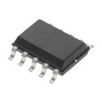
| 描述 | IC DAC STER 24BIT 192KHZ 10TSSOP音频数/模转换器 IC Stereo DAC 24-Bit 192kHz |
| 产品分类 | |
| 品牌 | Cirrus Logic |
| 产品手册 | |
| 产品图片 |
|
| rohs | 符合RoHS无铅 / 符合限制有害物质指令(RoHS)规范要求 |
| 产品系列 | 音频 IC,音频数/模转换器 IC,Cirrus Logic CS4344-CZZ- |
| 数据手册 | |
| 产品型号 | CS4344-CZZ |
| 产品目录页面 | |
| 产品种类 | 音频数/模转换器 IC |
| 位数 | 24 |
| 供应商器件封装 | 10-TSSOP |
| 其它名称 | 598-1051-5 |
| 分辨率 | 24 bit |
| 包装 | 管件 |
| 商标 | Cirrus Logic |
| 商标名 | CS4344 |
| 安装类型 | 表面贴装 |
| 安装风格 | SMD/SMT |
| 封装 | Tube |
| 封装/外壳 | 10-TFSOP,10-MSOP(0.118",3.00mm 宽) |
| 封装/箱体 | TSSOP-10 |
| 工作温度 | -10°C ~ 70°C |
| 工作温度范围 | - 10 C to + 70 C |
| 工作电源电压 | 3.3 V, 5 V |
| 工厂包装数量 | 96 |
| 建立时间 | - |
| 接口类型 | Serial |
| 数据接口 | 串行 |
| 最大功率耗散 | 69 mW |
| 标准包装 | 96 |
| 电压源 | 单电源 |
| 系列 | CS4344 |
| 转换器数 | 2 |
| 转换器数量 | 2 |
| 转换速率 | 192 kS/s |
| 输出数和类型 | 2 电压,单极 |
| 通道数量 | 2 Channel |
| 配用 | /product-detail/zh/CDB4344/598-1006-ND/923126 |
| 采样率(每秒) | 192k |


- 商务部:美国ITC正式对集成电路等产品启动337调查
- 曝三星4nm工艺存在良率问题 高通将骁龙8 Gen1或转产台积电
- 太阳诱电将投资9.5亿元在常州建新厂生产MLCC 预计2023年完工
- 英特尔发布欧洲新工厂建设计划 深化IDM 2.0 战略
- 台积电先进制程称霸业界 有大客户加持明年业绩稳了
- 达到5530亿美元!SIA预计今年全球半导体销售额将创下新高
- 英特尔拟将自动驾驶子公司Mobileye上市 估值或超500亿美元
- 三星加码芯片和SET,合并消费电子和移动部门,撤换高东真等 CEO
- 三星电子宣布重大人事变动 还合并消费电子和移动部门
- 海关总署:前11个月进口集成电路产品价值2.52万亿元 增长14.8%


PDF Datasheet 数据手册内容提取
CS4344/5/8 10-Pin, 24-Bit, 192 kHz Stereo D/A Converter Features Description Multi-bit Delta-Sigma Modulator The CS4344 family members (CS4344, CS4345, and CS4348) are complete, stereo digital-to-analog output 24-bit Conversion systems including interpolation, multibit D/A conversion and output analog filtering in a 10-pin package. The Automatically Detects Sample Rates up to CS4344 family supports major audio data interface for- 192 kHz. mats. Individual devices differ only in the supported interface format. 105 dB Dynamic Range The CS4344 family is based on a fourth-order multibit delta-sigma modulator with a linear analog low-pass fil- -90 dB THD+N ter. This family also includes autospeed mode detection using both sample rate and master clock ratio as a Low Clock-Jitter Sensitivity method of auto-selecting sampling rates between 2kHz and 200kHz. Single +3.3 or +5 V Power Supply The CS4344 family contains on-chip digital deempha- Filtered Line-Level Outputs sis, operates from a single +3.3V or +5V power supply, and requires minimal support circuitry. These features On-chip Digital De-emphasis are ideal for DVD players & recorders, digital televi- sions, home theater and set top box products, and Popguard® Technology automotive audio systems. The CS4344 family is available in a 10-pin TSSOP Small 10-pin TSSOP Package package in both Commercial (-10 to +85 °C) and Auto- motive grades (-40 to +85 °C). See Section 8. “Ordering Information” on page23 for complete details. 3.3 V or 5 V Switched Interpolation Multibit Capacitor Left De-emphasis Filter Modulator DAC and Output Filter Switched PCM Interpolation Multibit Capacitor Right Serial Audio Serial Filter Modulator DAC and Output Input Interface Filter Internal Voltage Reference Copyright Cirrus Logic, Inc. 2013 JUL ‘13 (All Rights Reserved) DS613F2 http://www.cirrus.com
CS4344/5/8 TABLE OF CONTENTS 1. PIN DESCRIPTIONS ..............................................................................................................................4 2. CHARACTERISTICS AND SPECIFICATIONS ......................................................................................5 SPECIFIED OPERATING CONDITIONS ...............................................................................................5 ABSOLUTE MAXIMUM RATINGS .........................................................................................................5 DAC ANALOG CHARACTERISTICS .....................................................................................................6 DAC ANALOG CHARACTERISTICS - ALL MODES .............................................................................6 COMBINED INTERPOLATION & ON-CHIP ANALOG FILTER RESPONSE ........................................7 DIGITAL INPUT CHARACTERISTICS ...................................................................................................8 POWER AND THERMAL CHARACTERISTICS ...................................................................................8 SWITCHING CHARACTERISTICS - SERIAL AUDIO INTERFACE ......................................................9 3. TYPICAL CONNECTION DIAGRAM ...................................................................................................11 4. APPLICATIONS ...................................................................................................................................12 4.1 Master Clock ...................................................................................................................................12 4.2 Serial Clock ....................................................................................................................................12 4.2.1 External Serial Clock Mode ...................................................................................................12 4.2.2 Internal Serial Clock Mode ....................................................................................................12 4.3 De-Emphasis ..................................................................................................................................15 4.4 Initialization and Power-Down ........................................................................................................15 4.5 Output Transient Control ................................................................................................................15 4.5.1 Power-Up ..............................................................................................................................15 4.5.2 Power-Down ..........................................................................................................................15 4.6 Grounding and Power Supply Decoupling ......................................................................................17 4.7 Analog Output and Filtering ............................................................................................................17 5. FILTER PLOTS .....................................................................................................................................18 6. PARAMETER DEFINITIONS ................................................................................................................21 7. PACKAGE DIMENSIONS ....................................................................................................................22 8. ORDERING INFORMATION ................................................................................................................23 8.1 Functional Compatibility .................................................................................................................23 8.2 Selection Guide ..............................................................................................................................23 9. REVISION HISTORY ............................................................................................................................24 2
CS4344/5/8 LIST OF FIGURES Figure 1.Output Test Load . . . . . . . . . . . . . . . . . . . . . . . . . . . . . . . . . . . . . . . . . . . . . . . . . . . . .8 Figure 2.Maximum Loading . . . . . . . . . . . . . . . . . . . . . . . . . . . . . . . . . . . . . . . . . . . . . . . . . . . .8 Figure 3.External Serial Mode Input Timing . . . . . . . . . . . . . . . . . . . . . . . . . . . . . . . . . . . . . . .10 Figure 4.Internal Serial Mode Input Timing . . . . . . . . . . . . . . . . . . . . . . . . . . . . . . . . . . . . . . .10 Figure 5.Internal Serial Clock Generation . . . . . . . . . . . . . . . . . . . . . . . . . . . . . . . . . . . . . . . .10 Figure 6.Typical Connection Diagram . . . . . . . . . . . . . . . . . . . . . . . . . . . . . . . . . . . . . . . . . . .11 Figure 7.CS4344 Data Format (I2S) . . . . . . . . . . . . . . . . . . . . . . . . . . . . . . . . . . . . . . . . . . . . .13 Figure 8.CS4345 Data Format (Left Justified) . . . . . . . . . . . . . . . . . . . . . . . . . . . . . . . . . . . . .13 Figure 9.CS4348 Data Format (Right Justified 16) . . . . . . . . . . . . . . . . . . . . . . . . . . . . . . . . .14 Figure 10.De-Emphasis Curve (Fs = 44.1kHz) . . . . . . . . . . . . . . . . . . . . . . . . . . . . . . . . . . . .15 Figure 11.CS4344/5/8 Initialization and Power-down Sequence . . . . . . . . . . . . . . . . . . . . . . .16 Figure 12.Single-Speed Stopband Rejection . . . . . . . . . . . . . . . . . . . . . . . . . . . . . . . . . . . . . .18 Figure 13.Single-Speed Transition Band . . . . . . . . . . . . . . . . . . . . . . . . . . . . . . . . . . . . . . . . .18 Figure 14.Single-Speed Transition Band . . . . . . . . . . . . . . . . . . . . . . . . . . . . . . . . . . . . . . . . .18 Figure 15.Single-Speed Passband Ripple . . . . . . . . . . . . . . . . . . . . . . . . . . . . . . . . . . . . . . . .18 Figure 16.Double-Speed Stopband Rejection . . . . . . . . . . . . . . . . . . . . . . . . . . . . . . . . . . . . .19 Figure 17.Double-Speed Transition Band . . . . . . . . . . . . . . . . . . . . . . . . . . . . . . . . . . . . . . . .19 Figure 18.Double-Speed Transition Band . . . . . . . . . . . . . . . . . . . . . . . . . . . . . . . . . . . . . . . .19 Figure 19.Double-Speed Passband Ripple . . . . . . . . . . . . . . . . . . . . . . . . . . . . . . . . . . . . . . .19 Figure 20.Quad-Speed Stopband Rejection . . . . . . . . . . . . . . . . . . . . . . . . . . . . . . . . . . . . . .20 Figure 21.Quad-Speed Transition Band . . . . . . . . . . . . . . . . . . . . . . . . . . . . . . . . . . . . . . . . . .20 Figure 22.Quad-Speed Transition Band . . . . . . . . . . . . . . . . . . . . . . . . . . . . . . . . . . . . . . . . . .20 Figure 23.Quad-Speed Passband Ripple . . . . . . . . . . . . . . . . . . . . . . . . . . . . . . . . . . . . . . . . .20 3
CS4344/5/8 1. PIN DESCRIPTIONS SDIN 1 10 AOUTR DEM/SCLK 2 9 VA LRCK 3 8 GND MCLK 4 7 AOUTL VQ 5 6 FILT+ Pin Name # Pin Description SDIN 1 Serial Audio Data Input (Input) - Input for two’s complement serial audio data. 2 De-Emphasis/External Serial Clock Input (Input) - used for deemphasis filter control or external serial DEM/SCLK clock input. 3 Left Right Clock (Input) - Determines which channel, Left or Right, is currently active on the serial audio LRCK data line. MCLK 4 Master Clock (Input) - Clock source for the delta-sigma modulator and digital filters. VQ 5 Quiescent Voltage (Output) - Filter connection for internal quiescent voltage. 6 Positive Voltage Reference (Output) - Positive reference voltage for the internal sampling FILT+ circuits. 7 Left Channel Analog Output (Output) - The full scale analog output level is specified in the Analog Char- AOUTL acteristics specification table. GND 8 Ground (Input) - ground reference. VA 9 Analog Power (Input) - Positive power for the analog and digital sections. 10 Right Channel Analog Output (Output) - The full scale analog output level is specified in the Analog AOUTR Characteristics specification table. 4
CS4344/5/8 2. CHARACTERISTICS AND SPECIFICATIONS (All Min/Max characteristics and specifications are guaranteed over the Specified Operating Conditions. Typical performance characteristics and specifications are derived from measurements taken at nominal supply voltage and T = 25C.) A SPECIFIED OPERATING CONDITIONS (AGND = 0V; all voltages with respect to ground.) Parameters Symbol Min Nom Max Units DC Power Supply VA 4.75 5.0 5.25 V 3.00 3.3 3.47 V Specified Temperature Range -CZZ T -10 - +70 C A -DZZ -40 - +85 C ABSOLUTE MAXIMUM RATINGS (AGND = 0V; all voltages with respect to ground.) Parameters Symbol Min Max Units DC Power Supply VA -0.3 6.0 V Input Current, Any Pin Except Supplies I - ±10 mA in Digital Input Voltage V -0.3 VA+0.4 V IND Ambient Operating Temperature (power applied) T -55 125 °C op Storage Temperature T -65 150 °C stg WARNING: Operation at or beyond these limits may result in permanent damage to the device. Normal operation is not guaranteed at these extremes. 5
CS4344/5/8 DAC ANALOG CHARACTERISTICS (Full-Scale Output Sine Wave, 997Hz (Note 1), Fs=48/96/192kHz; Test load R = 3k, C = 10pF (Figure1). L L Measurement Bandwidth 10 Hz to 20kHz, unless otherwise specified.) 5V Nom 3.3V Nom Parameter Min Typ Max Min Typ Max Unit Dynamic Performance for CS4344/5/8-CZZ (-10 to 70°C) Dynamic Range 18 to 24-Bit A-weighted 99 105 - 97 103 - dB unweighted 96 102 - 94 100 - dB 16-Bit A-weighted 90 96 - 90 96 - dB unweighted 87 93 - 87 93 - dB Total Harmonic Distortion + Noise 18 to 24-Bit 0 dB - -90 -85 - -90 -85 dB -20 dB - -82 -76 - -80 -74 dB -60 dB - -42 -36 - -40 -34 dB 16-Bit 0 dB - -90 -84 - -90 -84 dB -20 dB - -73 -67 - -73 -67 dB -60 dB - -33 -27 - -33 -27 dB Dynamic Performance for CS4344/5-DZZ (-40 to 85°C) Dynamic Range 18 to 24-Bit A-weighted 95 105 - 93 103 - dB unweighted 92 102 - 90 100 - dB 16-Bit A-weighted 86 96 - 86 96 - dB unweighted 83 93 - 83 93 - dB Total Harmonic Distortion + Noise 18 to 24-Bit 0 dB - -90 -82 - -90 -82 dB -20 dB - -82 -72 - -80 -70 dB -60 dB - -42 -32 - -40 -30 dB 16-Bit 0 dB - -90 -82 - -90 -82 dB -20 dB - -73 -63 - -73 -63 dB -60 dB - -33 -23 - -33 -23 dB Notes: 1. One LSB of triangular PDF dither added to data. DAC ANALOG CHARACTERISTICS - ALL MODES Parameter Symbol Min Typ Max Unit Interchannel Isolation (1kHz) - 100 - dB DC Accuracy Interchannel Gain Mismatch - 0.1 0.25 dB Gain Drift - 100 - ppm/°C Analog Output Full Scale Output Voltage 0.60•VA 0.65•VA 0.70•VA Vpp Quiescent Voltage V - 0.5•VA - VDC Q Max DC Current draw from an AOUT pin I - 10 - A OUTmax Max Current draw from VQ I - 100 - A Qmax Max AC-Load Resistance (see Figure 2 on page 8) R - 3 - k L Max Load Capacitance (see Figure 2 on page 8) C - 100 - pF L Output Impedance Z - 100 - OUT 6
CS4344/5/8 COMBINED INTERPOLATION & ON-CHIP ANALOG FILTER RESPONSE (The filter characteristics have been normalized to the sample rate (Fs) and can be referenced to the desired sam- ple rate by multiplying the given characteristic by Fs.) See (Note 6) Parameter Symbol Min Typ Max Unit Combined Digital and On-chip Analog Filter Response—Single-Speed Mode Passband (Note 2) to -0.1dB corner 0 - .35 Fs to -3dB corner 0 - .4992 Fs Frequency Response 10Hz to 20kHz -.175 - +.01 dB StopBand .5465 - - Fs StopBand Attenuation (Note 3) 50 - - dB Group Delay tgd - 10/Fs - s De-emphasis Error (Note 5) Fs = 32kHz - - +1.5/+0 dB Fs = 44.1 kHz - - +.05/-.25 dB Fs = 48 kHz - - -.2/-.4 dB Combined Digital and On-chip Analog Filter Response—Double-Speed Mode Passband (Note 2) to +0.1dB corner 0 - .22 Fs to -3dB corner 0 - .501 Fs Frequency Response 10Hz to 20kHz -.15 - +.15 dB StopBand .5770 - - Fs StopBand Attenuation (Note 3) 55 - - dB Group Delay tgd - 5/Fs - s Combined Digital and On-chip Analog Filter Response—Quad-Speed Mode Passband (Note 2) to -0.1dB corner 0 - 0.110 Fs to -3dB corner 0 - 0.469 Fs Frequency Response 10Hz to 20kHz -.12 - +0 dB StopBand 0.7 - - Fs StopBand Attenuation (Note 3) 51 - - dB Group Delay tgd - 2.5/Fs - s Notes: 2. Response is clock dependent and will scale with Fs. 3. For Single-Speed Mode, the Measurement Bandwidth is 0.5465 Fs to 3 Fs. For Double-Speed Mode, the Measurement Bandwidth is 0.577 Fs to 1.4 Fs. For Quad-Speed Mode, the Measurement Bandwidth is 0.7 Fs to 1 Fs. 4. Refer to Figure2. 5. De-emphasis is available only in Single-Speed Mode. 6. Amplitude vs. Frequency plots of this data are available in “Filter Plots” on page18. 7
CS4344/5/8 DIGITAL INPUT CHARACTERISTICS Parameters Symbol Min Typ Max Units High-Level Input Voltage (% of VA) V 60% - - V IH Low-Level Input Voltage (% of VA) V - - 30% V IL Input Leakage Current (Note 7) I - - ±10 A in Input Capacitance - 8 - pF 7. I for LRCK is ±20A max. in POWER AND THERMAL CHARACTERISTICS 5V Nom 3.3V Nom Parameters Symbol Min Typ Max Min Typ Max Units Power Supplies Power Supply Current normal operation I - 22 30 - 16 21 mA A (Note 8) power-down state (Note 9) I - 220 - - 100 - A A Power Dissipation normal operation - 110 150 - 53 69 mW power-down state(Note 9) - 1.1 - - 0.33 - mW Package Thermal Resistance - 95 - - 95 - °C/Watt JA Power Supply Rejection Ratio (Note 8) (1kHz) PSRR - 50 - - 50 - dB (60Hz) - 40 - - 40 - dB 8. Current consumption increases with increasing FS and increasing MCLK. Typ and Max values are based on highest FS and highest MCLK. Variance between speed modes is small. 9. Power down mode is defined when all clock and data lines are held static. 10. Valid with the recommended capacitor values on VQ and FILT+as shown in the typical connection di- agram in Section 3. 3.3µF AOUTx Vout R C L L AGND Figure 1. Output Test Load 125 pF) 100 C (L d -- 75 a o L Safe Operating ve 50 Region citi a p 25 a C 2.5 5 10 15 20 3 Resistive Load -- R L (k) Figure 2. Maximum Loading 8
CS4344/5/8 SWITCHING CHARACTERISTICS - SERIAL AUDIO INTERFACE Parameters Symbol Min Typ Max Units MCLK Frequency 0.512 - 50 MHz MCLK Duty Cycle 45 - 55 % Input Sample Rate All MCLK/LRCK ratios combined Fs 2 200 kHz (Note 11) 256x, 384x, 1024x 2 50 kHz 256x, 384x 84 134 kHz 512x, 768x 42 67 kHz 1152x 30 34 kHz 128x, 192x 50 100 kHz 64x, 96x 100 200 kHz 128x, 192x 168 200 kHz External SCLK Mode LRCK Duty Cycle (External SCLK only) 45 50 55 % SCLK Pulse Width Low t 20 - - ns sclkl SCLK Pulse Width High t 20 - - ns sclkh SCLK Duty Cycle 45 50 55 % SCLK rising to LRCK edge delay t 20 - - ns slrd SCLK rising to LRCK edge setup time t 20 - - ns slrs SDIN valid to SCLK rising setup time t 20 - - ns sdlrs SCLK rising to SDIN hold time t 20 - - ns sdh Internal SCLK Mode LRCK Duty Cycle (Internal SCLK only) (Note 12) - 50 - % SCLK Period (Note 13) t 109 - - ns sclkw ---------------- SCLK SCLK rising to LRCK edge tsclkr - t---s---c---l--k---w---- - ns 2 SDIN valid to SCLK rising setup time t 109 - - ns sdlrs ----------------------+10 512Fs SCLK rising to SDIN hold time t 109 - - ns MCLK / LRCK =1152, 1024, 512, 256, 128, or 64 sdh ----------------------+15 512Fs SCLK rising to SDIN hold time t 109 - - ns MCLK / LRCK = 768, 384, 192, or 96 sdh ----------------------+15 384Fs 11. Not all sample rates are supported for all clock ratios. See Table1, “Common Clock Frequencies,” on page12 for supported ratio’s and frequencies. 12. In Internal SCLK Mode, the Duty Cycle must be 50% 1/2 MCLK Period. 13. The SCLK / LRCK ratio may be either 32, 48, 64, or 72. This ratio depends on part type and MC- LK/LRCK ratio. (See Figures7-9) 9
CS4344/5/8 LRCK t t slrs sclkh t slrd t sclkl SCLK t t sdh sdlrs SDATA Figure 3. External Serial Mode Input Timing LRCK t sclkr SDATA t sclkw t t sdlrs sdh *INTERNAL SCLK The SCLK pulses shown are internal to the CS4344/5/8. Figure 4. Internal Serial Mode Input Timing LRCK MCLK 1 N N 2 *INTERNAL SCLK SDATA * The SCLK pulses shown are internal to the CS4344/5/8. N equals MCLK divided by SCLK Figure 5. Internal Serial Clock Generation 10
CS4344/5/8 3. TYPICAL CONNECTION DIAGRAM Note* = This circuitry is intended for applications where the CS4344/5/8 connects directly to an unbalanced output of the design. For internal routing applications please see the DAC analog output characteristics for loading limitations. +3.3 V to +5 V + 0.1µF 1µF 9 VA Note* 1 Audio SDIN 3.3µF 470 LeOftuAtpuudtio Data 2 DEM/SCLK AOUTL 7 Processor + 3 LRCK 10k C Rext 3.3µF 470 RightAudio CS4344 Output 10 CS4345 AOUTR + CS4348 10k C Rext 6 ExternalClock 4 MCLK FILT+ + 10µF C= 4RFexst(R+470470)For best 20 kHz response ext 5 VQ AGND *Popguard ramp can be adjusted by 8 0.1µF + *3.o3rµF s3e.3le µcFtin tgo tghivise c 2a5p0a cmitso rr avmalpu eti mtoe be *10µF or 10 µF to give a 420 ms ramp time. Figure 6. Typical Connection Diagram 11
CS4344/5/8 4. APPLICATIONS The CS4344 family accepts data at standard audio sample rates including 48, 44.1 and 32kHz in SSM, 96, 88.2 and 64kHz in DSM, and 192, 176.4 and 128kHz in QSM. Audio data is input via the serial data input pin (SDIN). The Left/Right Clock (LRCK) determines which channel is currently being input on SDIN, and the optional Serial Clock (SCLK) clocks audio data into the input data buffer. The CS4344/5/8 differ in serial data formats as shown in Figures7–9. 4.1 Master Clock MCLK/LRCK must be an integer ratio, as shown in Table1. The LRCK frequency is equal to Fs, the fre- quency at which words for each channel are input to the device. The MCLK-to-LRCK frequency ratio and speed mode is detected automatically during the initialization sequence by counting the number of MCLK transitions during a single LRCK period and by detecting the absolute speed of MCLK. Internal dividers are set to generate the proper clocks. Table1 illustrates several standard audio sample rates and the required MCLK and LRCK frequencies. Please note there is no required phase relationship, but MCLK, LRCK and SCLK must be synchronous. MCLK (MHz) LRCK 64x 96x 128x 192x 256x 384x 512x 768x 1024x 1152x (kHz) 32 - - - - 8.1920 12.2880 - - 32.7680 36.8640 44.1 - - - - 11.2896 16.9344 22.5792 33.8680 45.1580 - 48 - - - - 12.2880 18.4320 24.5760 36.8640 49.1520 - 64 - - 8.1920 12.2880 - - 32.7680 49.1520 - - 88.2 - - 11.2896 16.9344 22.5792 33.8680 - - - - 96 - - 12.2880 18.4320 24.5760 36.8640 - - - - 128 8.1920 12.2880 - - 32.7680 49.1520 - - - - 176.4 11.2896 16.9344 22.5792 33.8680 - - - - - - 192 12.2880 18.4320 24.5760 36.8640 - - - - - - Mode QSM DSM SSM Table 1. Common Clock Frequencies 4.2 Serial Clock The serial clock controls the shifting of data into the input data buffers. The CS4344 family supports both external and internal serial clock generation modes. Refer to Figures7–9 for data formats. 4.2.1 External Serial Clock Mode The CS4344 family will enter the External Serial Clock Mode when 16 low to high transitions are detected on the DEM/SCLK pin during any phase of the LRCK period. When this mode is enabled, the Internal Se- rial Clock Mode and deemphasis filter cannot be accessed. The CS4344 family will switch to Internal Se- rial Clock Mode if no low to high transitions are detected on the DEM/SCLK pin for 2 consecutive frames of LRCK. Refer to Figure11. 4.2.2 Internal Serial Clock Mode In the Internal Serial Clock Mode, the serial clock is internally derived and synchronous with MCLK and LRCK. The SCLK/LRCK frequency ratio is either 32, 48, 64, or 72 depending upon data format. Operation in this mode is identical to operation with an external serial clock synchronized with LRCK. This mode al- lows access to the digital deemphasis function. Refer to Figures7–11 for details. 12
CS4344/5/8 LRCK Left Channel Right Channel SCLK SDATA MSB-1 -2 -3 -4 -5 +5+4+3+2+1LSB MSB-1 -2 -3 -4 +5+4+3+2+1LSB Internal SCLK Mode External SCLK Mode I²S, 16-Bit data and INT SCLK = 32 Fs if I²S, up to 24-Bit Data MCLK/LRCK = 1024, 512, 256, 128, or 64 Data Valid on Rising Edge of SCLK I²S, Up to 24-Bit data and INT SCLK = 48 Fs if MCLK/LRCK = 768, 384, 192, or 96 I²S, Up to 24-Bit data and INT SCLK = 72 Fs if MCLK/LRCK = 1152 Figure 7. CS4344 Data Format (I2S) LRCK Left Channel Right Channel SCLK SDATA MSB-1 -2 -3 -4 -5 +5+4+3+2+1LSB MSB-1 -2 -3 -4 +5+4+3+2+1LSB Internal SCLK Mode External SCLK Mode Left-Justified, up to 24-Bit Data Left-Justified, up to 24-Bit Data INT SCLK = 64 Fs if Data Valid on Rising Edge of SCLK MCLK/LRCK = 1024, 512, 256, 128, or 64 INT SCLK = 48 Fs if MCLK/LRCK = 768, 384, 192, or 96 INT SCLK = 72 Fs if MCLK/LRCK = 1152 Figure 8. CS4345 Data Format (Left Justified) 13
CS4344/5/8 LRCK Left Channel Right Channel SCLK SDATA 151413121110 9 8 7 6 5 4 3 2 1 0 151413121110 9 8 7 6 5 4 3 2 1 0 Internal SCLK Mode External SCLK Mode 32 clocks Right Justified, 16-Bit Data Right Justified, 16-Bit Data INT SCLK = 32 Fs if Data Valid on Rising Edge of SCLK MCLK/LRCK = 1024, 512, 256, 128, or 64 SCLK Must Have at Least 32 Cycles per LRCK Period INT SCLK = 48 Fs if MCLK/LRCK = 768, 384, 192, or 96 INT SCLK = 72 Fs if MCLK/LRCK = 1152 Figure 9. CS4348 Data Format (Right Justified 16) 14
CS4344/5/8 4.3 De-Emphasis The CS4344 family includes on-chip digital deemphasis. Figure10 shows the deemphasis curve for Fs equal to 44.1 kHz. The frequency response of the deemphasis curve will scale proportionally with changes in sample rate, Fs. The deemphasis filter is active (inactive) if the DEM/SCLK pin is low (high) for 5 consecutive falling edges of LRCK. This function is available only in the internal serial clock mode . Gain dB T1=50 µs 0dB T2 = 15 µs -10dB F1 F2 Frequency 3.183 kHz 10.61 kHz Figure 10. De-Emphasis Curve (Fs = 44.1kHz) 4.4 Initialization and Power-Down The Initialization and Power-down sequence flow chart is shown in Figure11. The CS4344 family enters the Power-Down State upon initial power-up. The interpolation filters and delta-sigma modulators are reset, and the internal voltage reference, multi-bit digital-to-analog converters and switched-capacitor low-pass filters are pow- ered down. The device will remain in the Power-down mode until MCLK and LRCK are present. Once MCLK and LRCK are detected, MCLK occurrences are counted over one LRCK period to determine the MCLK/LRCK fre- quency ratio. Power is then applied to the internal voltage reference. Finally, power is applied to the D/A converters and switched-capacitor filters, and the analog outputs will ramp to the quiescent voltage, VQ. 4.5 Output Transient Control ® The CS4344 family uses Popguard technology to minimize the effects of output transients during power- up and power-down. This technique eliminates the audio transients commonly produced by single-ended single-supply converters when it is implemented with external DC-blocking capacitors connected in series with the audio outputs. To make best use of this feature, it is necessary to understand its operation. 4.5.1 Power-Up When the device is initially powered-up, the audio outputs, AOUTL and AOUTR, are clamped to VQ which is initially low. After MCLK is applied, the outputs begin to ramp with VQ towards the nominal quiescent voltage. This ramp takes approximately 250ms with a 3.3 µF cap connected to VQ (420ms with a 10µF connected to VQ) to complete. The gradual voltage ramping allows time for the external DC-blocking ca- pacitors to charge to VQ, effectively blocking the quiescent DC voltage. Once valid LRCK and SDIN are supplied (and SCLK if used) approximately 2000 sample periods later audio output begins. 4.5.2 Power-Down To prevent audio transients at power-down, the DC-blocking capacitors must fully discharge before turn- ing off the power. To accomplish this, MCLK should be stopped for a period of about 250ms for a 3.3µF cap connected to VQ (420ms for a 10µF cap connected to VQ) before removing power. During this time voltage on VQ and the audio outputs discharge gradually to GND. If power is removed before this time period has passed a transient will occur when the VA supply drops below that of VQ. There is no minimum time for a power cycle; power may be re-applied at any time. 15
CS4344/5/8 When changing clock ratio or sample rate, it is recommended that zero data (or near zero data) be present on SDIN for at least 10 LRCK samples before the change is made. During the clocking change, the DAC outputs will always be in a zero data state. If no zero audio is present at the time of switching, a slight click or pop may be heard as the DAC output automatically goes to its zero data state. USER: Apply Power VQ and outputs Power-Down State VQ and outputs ramp down VQ and outputs low ramp down USER: Apply MCLK USER: Remove USER: Remove MCLK MCLK VQ and outputs ramp up USER: Remove USER: Remove Wait State LRCK LRCK USER: Apply LRCK USER: change USER: change MCLK/LRCK Ratio Detection MCLK/LRCK ratio MCLK/LRCK ratio USER: No SCLK USER: Applied SCLK SCLK mode = internal SCLK mode = external Normal Operation Normal Operation De-emphasis De-emphasis available not available Analog Output Analog Output is Generated is Generated Figure 11. CS4344/5/8 Initialization and Power-down Sequence 16
CS4344/5/8 4.6 Grounding and Power Supply Decoupling As with any high resolution converter, the CS4344 family requires careful attention to power supply and grounding arrangements to optimize performance. Figure6 shows the recommended power arrangement with VA connected to a clean +3.3V or +5V supply. For best performance, decoupling and filter capacitors should be located as close to the device package as possible with the smallest capacitors closest. 4.7 Analog Output and Filtering The analog filter present in the CS4344 family is a switched-capacitor filter followed by a continuous time low pass filter. Its response, combined with that of the digital interpolator, is given in Figures12 - 19. The recommended external analog circuitry is shown in the “Typical Connection Diagram” on page11. 17
CS4344/5/8 5. FILTER PLOTS Figure 12. Single-Speed Stopband Rejection Figure 13. Single-Speed Transition Band 0 -1 0.05 -2 0 -3 -0.05 -4 Amplitude dB --65 Amplitude dB -0.1 -0.15 -7 -0.2 -8 -0.25 -9 -100.45 0.46 0.47 0.48 0.49 0.5 0.51 0.52 0.53 0.54 0.55 0 0.05 0.1 0.15 0.2 0.25 0.3 0.35 0.4 0.45 0.5 Frequency (normalized to Fs) Frequency (normalized to Fs) Figure 14. Single-Speed Transition Band Figure 15. Single-Speed Passband Ripple 18
CS4344/5/8 Figure 16. Double-Speed Stopband Rejection Figure 17. Double-Speed Transition Band 1 0.8 0 0.7 - 1 0.6 - 2 0.5 - 3 0.4 Amplitude dB -- 54 Amplitude dB 00..23 - 6 - 7 0.1 - 8 0 - 9 -0.1 - 100.45 0.46 0.47 0.48 0.49 0.5 0.51 0.52 0.53 0.54 0.55 -0.20 0.05 0.1 0.15 0.2 0.25 0.3 0.35 0.4 0.45 0.5 Frequency (normalized to Fs) Frequency (normalized to Fs) Figure 18. Double-Speed Transition Band Figure 19. Double-Speed Passband Ripple 19
CS4344/5/8 0 0 -10 -10 -20 -30 -20 -40 mplitude (dB) -50 mplitude (dB)-30 A -60 A-40 -70 -50 -80 -90 -60 -100 0 0.1 0.2 0.3 0.4 0.5 0.6 0.7 0.8 0.9 1 0.35 0.4 0.45 0.5 0.55 0.6 0.65 0.7 0.75 Frequency(normalized to Fs) Frequency(normalized to Fs) Figure 20. Quad-Speed Stopband Rejection Figure 21. Quad-Speed Transition Band 0 0 -5 -10 -15 -0.5 -20 mplitude (dB)-25 Amplitude dB A-30 -1 -35 -40 -45 -50 -1.5 0.4 0.45 0.5 0.55 0.6 0.65 0.7 0 0.05 0.1 0.15 0.2 0.25 0.3 0.35 0.4 0.45 0.5 Frequency(normalized to Fs) Frequency (normalized to Fs) Figure 22. Quad-Speed Transition Band Figure 23. Quad-Speed Passband Ripple 20
CS4344/5/8 6. PARAMETER DEFINITIONS Dynamic Range The ratio of the full scale rms value of the signal to the rms sum of all other spectral components over the specified bandwidth. Dynamic range is a signal-to-noise measurement over the specified bandwidth made with a -60dBFS signal. 60dB is then added to the resulting measurement to refer the measure- ment to full scale. This technique ensures that the distortion components are below the noise level and do not affect the measurement. This measurement technique has been accepted by the Audio Engineer- ing Society, AES17-1991, and the Electronic Industries Association of Japan, EIAJ CP-307. Gain Drift The change in gain value with temperature. Units in ppm/°C. Gain Error The deviation from the nominal full scale analog output for a full scale digital input. Interchannel Gain Mismatch The gain difference between left and right channels. Units in decibels. Interchannel Isolation A measure of crosstalk between the left and right channels. Measured for each channel at the converter's output with all zeros to the input under test and a full-scale signal applied to the other channel. Units in decibels. Total Harmonic Distortion + Noise (THD+N) The ratio of the rms value of the signal to the rms sum of all other spectral components over the specified bandwidth (typically 10Hz to 20kHz), including distortion components. Expressed in decibels. 21
CS4344/5/8 7. PACKAGE DIMENSIONS 10LD TSSOP (3 mm BODY) PACKAGE DRAWING N D E11 c E A2 A A1 e b L END VIEW SEATING SIDE VIEW PLANE L1 1 2 3 TOP VIEW INCHES MILLIMETERS NOTE DIM MIN NOM MAX MIN NOM MAX A -- -- 0.0433 -- -- 1.10 A1 0 -- 0.0059 0 -- 0.15 A2 0.0295 -- 0.0374 0.75 -- 0.95 b 0.0059 -- 0.0118 0.15 -- 0.30 4, 5 c 0.0031 -- 0.0091 0.08 -- 0.23 D -- 0.1181 BSC -- -- 3.00 BSC -- 2 E -- 0.1929 BSC -- -- 4.90 BSC -- E1 -- 0.1181 BSC -- -- 3.00 BSC -- 3 e -- 0.0197 BSC -- -- 0.50 BSC -- L 0.0157 0.0236 0.0315 0.40 0.60 0.80 L1 -- 0.0374 REF -- -- 0.95 REF -- 0° -- 8° 0° -- 8° Controlling Dimension is Millimeters Notes: 1. Reference document: JEDEC MO-187 2. D does not include mold flash or protrusions which is 0.15 mm max. per side. 3. E1 does not include inter-lead flash or protrusions which is 0.15 mm max per side. 4. Dimension b does not include a total allowable dambar protrusion of 0.08 mm max. 5. Exceptions to JEDEC dimension. 22
CS4344/5/8 8. ORDERING INFORMATION Product Description Package Pb-Free Grade Temp Range Container Order # Commercial -10 to +70 °C CS4344-CZZ CS4344 24-Bit, 192kHz Automotive -40 to +85 °C Tube CS4344-DZZ Stereo D/A 10-TSSOP Yes Commercial -10 to +70 °C or CS4345-CZZ CS4345 Converter Automotive -40 to +85 °C Tape and Reel CS4345-DZZ CS4348 Commercial -10 to +70 °C CS4348-CZZ 8.1 Functional Compatibility CS4334-KS CS4344-CZZ CS4335-KS CS4345-CZZ CS4338-KS CS4348-CZZ CS4334-BS CS4344-DZZ CS4334-DS CS4344-DZZ 8.2 Selection Guide The CS4344 family differs by Serial Audio format as follows: • CS4344 — 16- to 24-bit, I²S • CS4345 — 16- to 24-bit, Left-Justified • CS4348 — 16-bit, Right-Justified 23
CS4344/5/8 9. REVISION HISTORY Release Changes -Updated passband and frequency response specifications in “Combined Interpolation & On-chip Analog Filter Response” on page7 F1 -Updated PSRR specification -Updated VIH specification -Updated figures in “Filter Plots” on page18 -Removed references to CS4346 throughout. -Updated Footnote 1 about dither in “DAC Analog Characteristics” on page6. F2 -Updated the “SCLK rising to LRCK edge” unit froms to ns in “Switching Characteristics - Serial Audio Interface” on page9. Contacting Cirrus Logic Support For all product questions and inquiries contact a Cirrus Logic Sales Representative. To find the one nearest to you go to www.cirrus.com/corporate/contacts/sales.cfm IMPORTANT NOTICE Cirrus Logic, Inc. and its subsidiaries ("Cirrus") believe that the information contained in this document is accurate and reliable. However, the information is subject to change without notice and is provided "AS IS" without warranty of any kind (express or implied). Customers are advised to obtain the latest version of relevant information to verify, before placing orders, that information being relied on is current and complete. All products are sold subject to the terms and conditions of sale supplied at the time of order acknowledgment, including those pertaining to warranty, indemnification, and limitation of liability. No responsibility is assumed by Cirrus for the use of this information, including use of this information as the basis for manufacture or sale of any items, or for infringement of patents or other rights of third parties. This document is the property of Cirrus and by furnishing this information, Cirrus grants no license, express or implied under any patents, mask work rights, copyrights, trademarks, trade secrets or other intellectual property rights. Cirrus owns the copyrights associated with the information contained herein and gives con- sent for copies to be made of the information only for use within your organization with respect to Cirrus integrated circuits or other products of Cirrus. This consent does not extend to other copying such as copying for general distribution, advertising or promotional purposes, or for creating any work for resale. CERTAIN APPLICATIONS USING SEMICONDUCTOR PRODUCTS MAY INVOLVE POTENTIAL RISKS OF DEATH, PERSONAL INJURY, OR SEVERE PROP- ERTY OR ENVIRONMENTAL DAMAGE (“CRITICAL APPLICATIONS”). CIRRUS PRODUCTS ARE NOT DESIGNED, AUTHORIZED OR WARRANTED FOR USE IN AIRCRAFT SYSTEMS, MILITARY APPLICATIONS, PRODUCTS SURGICALLY IMPLANTED INTO THE BODY, AUTOMOTIVE SAFETY OR SECURITY DE- VICES, LIFE SUPPORT PRODUCTS OR OTHER CRITICAL APPLICATIONS. INCLUSION OF CIRRUS PRODUCTS IN SUCH APPLICATIONS IS UNDERSTOOD TO BE FULLY AT THE CUSTOMER’S RISK AND CIRRUS DISCLAIMS AND MAKES NO WARRANTY, EXPRESS, STATUTORY OR IMPLIED, INCLUDING THE IMPLIED WARRANTIES OF MERCHANTABILITY AND FITNESS FOR PARTICULAR PURPOSE, WITH REGARD TO ANY CIRRUS PRODUCT THAT IS USED IN SUCH A MANNER. IF THE CUSTOMER OR CUSTOMER’S CUSTOMER USES OR PERMITS THE USE OF CIRRUS PRODUCTS IN CRITICAL APPLICA- TIONS, CUSTOMER AGREES, BY SUCH USE, TO FULLY INDEMNIFY CIRRUS, ITS OFFICERS, DIRECTORS, EMPLOYEES, DISTRIBUTORS AND OTHER AGENTS FROM ANY AND ALL LIABILITY, INCLUDING ATTORNEYS’ FEES AND COSTS, THAT MAY RESULT FROM OR ARISE IN CONNECTION WITH THESE USES. Cirrus Logic, Cirrus, the Cirrus Logic logo designs, and Popguard are trademarks of Cirrus Logic, Inc. All other brand and product names in this document may be trademarks or service marks of their respective owners. 24
Mouser Electronics Authorized Distributor Click to View Pricing, Inventory, Delivery & Lifecycle Information: C irrus Logic: CDB4344 CS4344-CZZ CS4344-CZZR CS4344-DZZ CS4344-DZZR CS4345-CZZ CS4345-CZZR CS4345-DZZ CS4345-DZZR CS4348-CZZ CS4348-CZZR