ICGOO在线商城 > 集成电路(IC) > 数据采集 - ADCs/DAC - 专用型 > AD1877JRZ
 Datasheet下载
- 型号: AD1877JRZ
- 制造商: Analog
- 库位|库存: xxxx|xxxx
- 要求:
| 数量阶梯 | 香港交货 | 国内含税 |
| +xxxx | $xxxx | ¥xxxx |
查看当月历史价格
查看今年历史价格
AD1877JRZ产品简介:
ICGOO电子元器件商城为您提供AD1877JRZ由Analog设计生产,在icgoo商城现货销售,并且可以通过原厂、代理商等渠道进行代购。 AD1877JRZ价格参考¥102.73-¥148.70。AnalogAD1877JRZ封装/规格:数据采集 - ADCs/DAC - 专用型, ADC,音频 16 b 48k 串行 28-SOIC。您可以下载AD1877JRZ参考资料、Datasheet数据手册功能说明书,资料中有AD1877JRZ 详细功能的应用电路图电压和使用方法及教程。
AD1877JRZ 是由 Analog Devices Inc.(ADI)生产的一款专用型数据采集芯片,属于 ADC/DAC 类产品。它是一款高精度、低功耗的音频编解码器(Codec),集成了立体声 16 位模数转换器(ADC)和数模转换器(DAC),广泛应用于需要高质量音频处理的场景。以下是 AD1877JRZ 的主要应用场景:

 1. 消费类电子产品
   - 便携式音频设备:如 MP3 播放器、录音笔等,AD1877JRZ 提供高质量的音频录制和回放功能。
   - 家用音响系统:用于数字音频输入/输出,支持 CD 质量的音频信号处理。
   - 耳机放大器:提供低失真、高保真的音频输出。

 2. 通信设备
   - VoIP 设备:在基于 IP 的语音通信中,AD1877JRZ 可以实现高质量的语音信号数字化和还原。
   - 电话会议系统:用于音频信号的采集和播放,确保清晰的语音传输。
   - 无线通信终端:如对讲机或移动基站中的音频处理模块。

 3. 工业控制与自动化
   - 人机界面(HMI)设备:在工业控制系统中,用于语音提示或音频报警功能。
   - 音频监控系统:用于实时采集和记录现场声音信息。

 4. 医疗设备
   - 助听器或听力辅助设备:提供高精度的声音采集和处理能力。
   - 医疗监护仪:用于心音、呼吸音等生物信号的数字化处理。

 5. 汽车电子
   - 车载娱乐系统:支持高品质的音频输入/输出,提升车内娱乐体验。
   - 语音识别系统:用于采集驾驶员或乘客的语音指令。

 6. 测试与测量
   - 音频分析仪:用于评估音频设备的性能,如扬声器或麦克风的频率响应。
   - 信号发生器:生成精确的音频测试信号。

AD1877JRZ 的特点包括低功耗设计、高信噪比(SNR)、内置采样率转换器以及灵活的接口选项(如 I²S、SPI 等),使其非常适合需要高性能音频处理的应用场景。
| 参数 | 数值 |
| ADC输入端数量 | 2 |
| 产品目录 | 集成电路 (IC)半导体 |
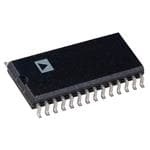
| 描述 | IC ADC STEREO 16BIT 28-SOIC音频模/数转换器 IC IC 16-Bit Stereo |
| 产品分类 | |
| 品牌 | Analog Devices |
| 产品手册 | |
| 产品图片 |
|
| rohs | 符合RoHS无铅 / 符合限制有害物质指令(RoHS)规范要求 |
| 产品系列 | 音频 IC,音频模/数转换器 IC,Analog Devices AD1877JRZ- |
| 数据手册 | |
| 产品型号 | AD1877JRZ |
| THD+噪声 | 90 dB |
| 产品目录页面 | |
| 产品种类 | 音频模/数转换器 IC |
| 供应商器件封装 | 28-SOIC W |
| 分辨率 | 16 bit |
| 分辨率(位) | 16 b |
| 功耗 | 255 mW |
| 包装 | 管件 |
| 商标 | Analog Devices |
| 安装类型 | 表面贴装 |
| 安装风格 | SMD/SMT |
| 封装 | Tube |
| 封装/外壳 | 28-SOIC(0.295",7.50mm 宽) |
| 封装/箱体 | SOIC-28 |
| 工作温度 | 0°C ~ 70°C |
| 工作电源电压 | 5 V |
| 工厂包装数量 | 27 |
| 数据接口 | 串行 |
| 最大功率耗散 | 315 mW |
| 最大工作温度 | + 70 C |
| 最小工作温度 | 0 C |
| 标准包装 | 27 |
| 电压-电源 | 4.75 V ~ 5.25 V |
| 电压源 | 模拟和数字 |
| 电源电压-最大 | 5.25 V |
| 电源电压-最小 | 4.75 V |
| 电源电流 | 80 mA |
| 类型 | ADC, 音频 |
| 系列 | AD1877 |
| 转换器数量 | 2 |
| 转换速率 | 48 kHz |
| 通道数量 | 2 Channel |
| 采样率(每秒) | 48k |


- 商务部:美国ITC正式对集成电路等产品启动337调查
- 曝三星4nm工艺存在良率问题 高通将骁龙8 Gen1或转产台积电
- 太阳诱电将投资9.5亿元在常州建新厂生产MLCC 预计2023年完工
- 英特尔发布欧洲新工厂建设计划 深化IDM 2.0 战略
- 台积电先进制程称霸业界 有大客户加持明年业绩稳了
- 达到5530亿美元!SIA预计今年全球半导体销售额将创下新高
- 英特尔拟将自动驾驶子公司Mobileye上市 估值或超500亿美元
- 三星加码芯片和SET,合并消费电子和移动部门,撤换高东真等 CEO
- 三星电子宣布重大人事变动 还合并消费电子和移动部门
- 海关总署:前11个月进口集成电路产品价值2.52万亿元 增长14.8%


PDF Datasheet 数据手册内容提取
a Single-Supply (cid:1)(cid:2) 16-Bit Stereo ADC AD1877 FEATURES FUNCTIONAL BLOCK DIAGRAM Single 5 V Power Supply Single-Ended Dual-Channel Analog Inputs 92 dB (Typ) Dynamic Range CLOCK LRCK 1 SERIAL OUTPUT DIVIDER 28 CLKIN 90 dB (Typ) S/(THD+N) INTERFACE 0.006 dB Decimator Passband Ripple WCLK 2 27 TAG Fourth-Order, 64-Times Oversampling (cid:1)(cid:2) Modulator BCLK 3 26 SOUT Three-Stage, Linear-Phase Decimator 256 (cid:3) FS or 384 (cid:3) FS Input Clock DVDD1 4 THRDEEEC-ISMTAATGIOEN FIR THRDEEEC-ISMTAATGIOEN FIR 25 DVDD2 Less than 100 (cid:4)W (Typ) Power-Down Mode DGND1 5 FILTER FILTER 24 DGND2 Input Overrange Indication RDEDGE 6 23 RESET On-Chip Voltage Reference D D D D Flexible Serial Output Interface S/M 7 AC AC AC AC 22 MSBDLY 28-Lead SOIC Package 384/256 8 21 RLJUST APPLICATIONS AVDD 9 20 AGND Consumer Digital Audio Receivers Digital Audio Recorders, Including Portables VINL 10 19 VINR CD-R, DCC, MD and DAT CAPL1 11 18 CAPR1 Multimedia and Consumer Electronic Equipment Sampling Music Synthesizers CAPL2 12 SINGLE TO SINGLE TO 17 CAPR2 DIFFERENTIAL INPUT DIFFERENTIAL INPUT Digital Karaoke Systems AGNDL 13 CONVERTER CONVERTER 16 AGNDR VREFL 14 RVEOFELRTAEGNCEE 15 VREFR AD1877 PRODUCT OVERVIEW The AD1877 is a stereo, 16-bit oversampling ADC based on Sigma Delta (∑∆) technology intended primarily for digital audio bandwidth applications requiring a single 5 V power supply. one-bit comparator’s quantization noise out of the audio pass- Each single-ended channel consists of a fourth-order one-bit band. The high order of the modulator randomizes the modulator noise shaping modulator and a digital decimation filter. An on- output, reducing idle tones in the AD1877 to very low levels. chip voltage reference, stable over temperature and time, defines Because its modulator is single-bit, AD1877 is inherently the full-scale range for both channels. Digital output data from monotonic and has no mechanism for producing differential both channels are time-multiplexed to a single, flexible serial linearity errors. interface. The AD1877 accepts a 256 × FS or a 384 × FS input The input section of the AD1877 uses autocalibration to correct clock (FS is the sampling frequency) and operates in both serial any dc offset voltage present in the circuit, provided that the inputs port “master” and “slave” modes. In slave mode, all clocks must are ac coupled. The single-ended dc input voltage can swing be externally derived from a common source. between 0.7 V and 3.8 V typically. The AD1877 antialias input Input signals are sampled at 64 × F onto internally buffered circuit requires four external 470 pF NPO ceramic chip filter S switched-capacitors, eliminating external sample-and-hold ampli- capacitors, two for each channel. No active electronics are fiers and minimizing the requirements for antialias filtering at the needed. Decoupling capacitors for the supply and reference pins input. With simplified antialiasing, linear phase can be preserved are also required. across the passband. The on-chip single-ended to differential signal The dual digital decimation filters are triple-stage, finite impulse converters save the board designer from having to provide them response filters for effectively removing the modulator’s high externally. The AD1877’s internal differential architecture provides frequency quantization noise and reducing the 64 × F single-bit S increased dynamic range and excellent power supply rejection output data rate to an F word rate. They provide linear phase S characteristics. The AD1877’s proprietary fourth-order differen- and a narrow transition band that properly digitizes 20 kHz signals tial switched-capacitor ∑∆ modulator architecture shapes the at a 44.1 kHz sampling frequency. Passband ripple is less than 0.006 dB, and stopband attenuation exceeds 90 dB. (Continued on Page 6) REV.A IInformation furnished by Analog Devices is believed to be accurate and reliable. However, no responsibility is assumed by Analog Devices for its use, nor for any infringements of patents or other rights of third parties One Technology Way, P.O. Box 9106, Norwood, MA 02062-9106, U.S.A. which may result from its use. No license is granted by implication or Tel: 781/329-4700 World Wide Web Site: http://www.analog.com otherwise under any patent or patent rights of Analog Devices. Fax: 781/326-8703 © Analog Devices, Inc., 2000
AD1877–SPECIFICATIONS TEST CONDITIONS UNLESS OTHERWISE NOTED Supply Voltages 5.0 V Ambient Temperature 25 °C Input Clock (F ) [256 × F ] 12.288 MHz CLKIN S Input Signal 991.768 Hz –0.5 dB Full Scale Measurement Bandwidth 23.2 Hz to 19.998 kHz Load Capacitance on Digital Outputs 50 pF Input Voltage HI (V ) 2.4 V IH Input Voltage LO (V ) 0.8 V IL Master Mode, Data I2S-Justified (Refer to Figure 14). Device Under Test (DUT) bypassed and decoupled as shown in Figure 3. DUT is antialiased and ac coupled as shown in Figure 2. DUT is calibrated. Values in bold typeface are tested, all others are guaranteed but not tested. ANALOG PERFORMANCE Min Typ Max Unit Resolution 16 Bits Dynamic Range (20 Hz to 20 kHz, –60 dB Input) Without A-Weight Filter 87 92 dB With A-Weight Filter 90 94 dB Signal to (THD + Noise) 86.5 90 dB Signal to THD 92 94 dB Analog Inputs Single-Ended Input Range (± Full Scale)* V – 1.55 V V + 1.55 V REF REF REF Input Impedance at Each Input Pin 32 kΩ V 2.05 2.25 2.55 V REF DC Accuracy Gain Error ±0.5 (cid:5)2.5 % Interchannel Gain Mismatch 0.01 dB Gain Drift 115 ppm/°C Midscale Offset Error (After Calibration) ±3 (cid:5)20 LSBs Midscale Drift 15 ppm/°C Crosstalk (EIAJ Method) –90 –99 dB *V p-p = V × 1.333. IN REF –2– REV. A
AD1877 DIGITAL I/O Min Typ Max Unit Input Voltage HI (V ) 2.4 V IH Input Voltage LO (V ) 0.8 V IL Input Leakage (I @ V = 5 V) 10 µA IH IH Input Leakage (I @ V = 0 V) 10 µA IL IL Output Voltage HI (V @ I = –2 mA) 2.4 V OH OH Output Voltage LO (V @ I = 2 mA) 0.4 V OL OL Input Capacitance 15 pF DIGITAL TIMING (Guaranteed over 0°C to 70°C, DV = AV = 5 V ± 5%. Refer to Figures 17–19.) DD DD Min Typ Max Unit t CLKIN Period 48 81 780 ns CLKIN F CLKIN Frequency (1/t ) 1.28 12.288 20.48 MHz CLKIN CLKIN t CLKIN LO Pulsewidth 15 ns CPWL t CLKIN HI Pulsewidth 15 ns CPWH t RESET LO Pulsewidth 50 ns RPWL t BCLK LO Pulsewidth 15 ns BPWL t BCLK HI Pulsewidth 15 ns BPWH t CLKIN Rise to BCLK Xmit (Master Mode) 15 ns DLYCKB t BCLK Xmit to LRCK Transition (Master Mode) 15 ns DLYBLR t BCLK Xmit to WCLK Rise 10 ns DLYBWR t BCLK Xmit to WCLK Fall 10 ns DLYBWF t BCLK Xmit to Data/Tag Valid (Master Mode) 10 ns DLYDT t LRCK Setup to BCLK Sample (Slave Mode) 10 ns SETLRBS t LRCK Transition to Data/TAG Valid (Slave Mode) DLYLRDT No MSB Delay Mode (for MSB Only) 40 ns t WCLK Setup to BCLK Sample (Slave Mode) SETWBS Data Position Controlled by WCLK Input Mode 10 ns t BCLK Xmit to DATA/TAG Valid (Slave Mode) DLYBDT All Bits Except MSB in No MSB Delay Mode All Bits in MSB Delay Mode 10 ns POWER Min Typ Max Unit Supplies Voltage, Analog and Digital 4.75 5 5.25 V Analog Current 35 43 mA Analog Current—Power Down (CLKIN Running) 6 26 µA Digital Current 16 20 mA Digital Current—Power Down (CLKIN Running) 13 39 µA Dissipation Operation—Both Supplies 255 315 mW Operation—Analog Supply 175 215 mW Operation—Digital Supply 80 100 mW Power Down—Both Supplies (CLKIN Running) 95 325 µW Power Down—Both Supplies (CLKIN Not Running) 5 µW Power Supply Rejection (See TPC 5) 1 kHz 300 mV p-p Signal at Analog Supply Pins 76 dB 20 kHz 300 mV p-p Signal at Analog Supply Pins 71 dB Stopband (≥0.55 × F )—any 300 mV p-p Signal 80 dB S REV. A –3–
AD1877 TEMPERATURE RANGE Min Typ Max Unit Specifications Guaranteed 25 °C Functionality Guaranteed 0 70 °C Storage –60 +100 °C DIGITAL FILTER CHARACTERISTICS Min Typ Max Unit Decimation Factor 64 Passband Ripple 0.006 dB Stopband1 Attenuation 90 dB 48 kHz F (at Recommended Crystal Frequencies) S Passband 0 21.6 kHz Stopband 26.4 kHz 44.1 kHz F (at Recommended Crystal Frequencies) S Passband 0 20 kHz Stopband 24.25 kHz 32 kHz F (at Recommended Crystal Frequencies) S Passband 0 14.4 kHz Stopband 17.6 kHz Other F S Passband 0 0.45 F S Stopband 0.55 F S Group Delay 36/F s S Group Delay Variation 0 µs NOTES 1Stopband repeats itself at multiples of 64 × F, where F is the output word rate. Thus the digital filter will attenuate to 0 dB across the frequency spectrum except S S for a range ±0.55 × F wide at multiples of 64 × F. S S Specifications subject to change without notice. ABSOLUTE MAXIMUM RATINGS Min Typ Max Unit DV 1 to DGND1 and DV 2 to DGND2 0 6 V DD DD AV to AGND/AGNDL/AGNDR 0 6 V DD Digital Inputs DGND – 0.3 DV + 0.3 V DD Analog Inputs AGND – 0.3 AV + 0.3 V DD AGND to DGND –0.3 +0.3 V Reference Voltage Indefinite Short Circuit to Ground Soldering (10 sec) 300 °C CAUTION ESD (electrostatic discharge) sensitive device. Electrostatic charges as high as 4000V readily WARNING! accumulate on the human body and test equipment and can discharge without detection. Although the AD1877 features proprietary ESD protection circuitry, permanent damage may occur on devices subjected to high-energy electrostatic discharges. Therefore, proper ESD precautions are recommended to avoid performance degradation or loss of functionality. ESD SENSITIVE DEVICE ORDERING GUIDE Package Package Model Temperature Description Option AD1877JR 0°C to 70°C SOIC R-28 –4– REV. A
AD1877 PIN FUNCTION DESCRIPTIONS Signal to Total Harmonic Distortion (S/THD) The ratio of the rms value of the fundamental input signal to the Input/ Pin rms sum of all harmonically related spectral components in the Pin Output Name Description passband, expressed in decibels. 1 I/O LRCK Left/Right Clock Passband 2 I/O WCLK Word Clock The region of the frequency spectrum unaffected by the attenu- 3 I/O BCLK Bit Clock ation of the digital decimator’s filter. 4 I DV 1 5 V Digital Supply Passband Ripple DD 5 I DGND1 Digital Ground The peak-to-peak variation in amplitude response from equal- amplitude input signal frequencies within the passband, 6 I RDEDGE Read Edge Polarity Select expressed in decibels. 7 I S/M Slave/Master Select Stopband 8 I 384/256 Clock Mode The region of the frequency spectrum attenuated by the digital 9 I AV 5 V Analog Supply DD decimator’s filter to the degree specified by “stopband 10 I VINL Left Channel Input attenuation.” 11 O CAPL1 Left External Filter Capacitor 1 Gain Error 12 O CAPL2 Left External Filter Capacitor 2 With a near full-scale input, the ratio of actual output to 13 I AGNDL Left Analog Ground expected output, expressed as a percentage. 14 O V L Left Reference Voltage Output REF Interchannel Gain Mismatch 15 O V R Right Reference Voltage Output With identical near full-scale inputs, the ratio of outputs of the REF 16 I AGNDR Right Analog Ground two stereo channels, expressed in decibels. 17 O CAPR2 Right External Filter Capacitor 2 Gain Drift 18 O CAPR1 Right External Filter Capacitor 1 Change in response to a near full-scale input with a change in 19 I V R Right Channel Input temperature, expressed as parts-per-million (ppm) per °C. IN 20 I AGND Analog Ground Midscale Offset Error 21 I RLJUST Right/Left Justify Output response to a midscale dc input, expressed in least- significant bits (LSBs). 22 I MSBDLY Delay MSB One BCLK Period 23 I RESET Reset Midscale Drift Change in midscale offset error with a change in temperature, 24 I DGND2 Digital Ground expressed as parts-per-million (ppm) per °C. 25 I DV 2 5 V Digital Supply DD Crosstalk (EIAJ Method) 26 O SOUT Serial Data Output Ratio of response on one channel with a grounded input to a 27 O TAG Serial Overrange Output full-scale 1 kHz sine-wave input on the other channel, expressed 28 I CLKIN Master Clock in decibels. Power Supply Rejection DEFINITIONS With no analog input, signal present at the output when a Dynamic Range 300 mV p-p signal is applied to power supply pins, expressed in The ratio of a full-scale output signal to the integrated output decibels of full scale. noise in the passband (20 Hz to 20 kHz), expressed in decibels Group Delay (dB). Dynamic range is measured with a –60 dB input signal Intuitively, the time interval required for an input pulse to and is equal to (S/[THD+N]) 60 dB. Note that spurious har- appear at the converter’s output, expressed in milliseconds monics are below the noise with a –60 dB input, so the noise (ms). More precisely, the derivative of radian phase with respect level establishes the dynamic range. The dynamic range is speci- to radian frequency at a given frequency. fied with and without an A-Weight filter applied. Group Delay Variation Signal to (Total Harmonic Distortion + Noise) The difference in group delays at different input frequencies. (S/(THD + N)) Specified as the difference between largest and the smallest The ratio of the root-mean-square (rms) value of the fundamen- group delays in the passband, expressed in microseconds (µs). tal input signal to the rms sum of all other spectral components in the passband, expressed in decibels (dB). REV. A –5–
AD1877 (Continued from Page 1 ) offset and indirect dependence on temperature and time as it affects dc offset. The AD1877 suppresses idle tones 20 dB or The flexible serial output port produces data in twos-comple- better below the integrated noise floor. ment, MSB-first format. The input and output signals are TTL compatible. The port is configured by pin selections. Each 16-bit The AD1877’s modulator was designed, simulated, and exhaus- output word of a stereo pair can be formatted within a 32-bit tively tested to remain stable for any input within a wide tolerance field of a 64-bit frame as either right-justified, I2S-compatible, of its rated input range. The AD1877 is designed to internally Word Clock controlled or left-justified positions. Both 16-bit reset itself should it ever be overdriven, to prevent it from going samples can also be packed into a 32-bit frame, in left-justified instable. It will reset itself within 5 µs at a 48 kHz sampling and I2S-compatible positions. frequency after being overdriven. Overdriving the inputs will produce a waveform “clipped” to plus or minus full scale. The AD1877 is fabricated on a single monolithic integrated circuit using a 0.8 µm CMOS double polysilicon, double metal process, See TPCs 1 through 16 for illustrations of the AD1877’s and is offered in a plastic 28-lead SOIC package. Analog and typical analog performance as measured by an Audio Precision digital supply connections are separated to isolate the analog cir- System One. Signal-to(distortion + noise) is shown under a cuitry from the digital supply and reduce digital crosstalk. range of conditions. Note that there is a small variance between the AD1877 analog performance specifications and some of the The AD1877 operates from a single 5 V power supply over the temperature range of 0°C to 70°C, and typically consumes less performance plots. This is because the Audio Precision System One measures THD and noise over a 20 Hz to 24 kHz band- than 260 mW of power. width, while the analog performance is specified over a 20 Hz to 20 kHz bandwidth (i.e., the AD1877 performs slightly better THEORY OF OPERATION (cid:1)(cid:2) Modulator Noise-Shaping than the plots indicate). The power supply rejection (TPC 5) graph illustrates the benefits of the AD1877’s internal differen- The stereo, internally differential analog modulator of the tial architecture. The excellent channel separation shown in AD1877 employs a proprietary feedforward and feedback archi- TPC 6 is the result of careful chip design and layout. tecture that passes input signals in the audio band with a unity transfer function yet simultaneously shapes the quantization Digital Filter Characteristics noise generated by the one-bit comparator out of the audio The digital decimator accepts the modulator’s stereo bitstream band. See Figure 1. Without the ∑∆ architecture, this quantiza- and simultaneously performs two operations on it. First, the tion noise would be spread uniformly from dc to one-half the decimator low-pass filters the quantization noise that the modu- oversampling frequency, 64 × F . lator shaped to high frequencies and filters any other out-of S audio-band input signals. Second, it reduces the data rate to an (cid:6)VIN output word rate equal to F . The high frequency bitstream is S DAC decimated to stereo 16-bit words at 48 kHz (or other desired MODULATOR FS). The out-of-band one-bit quantization noise and other high BITSTREAM VIN SINGLE TO OUTPUT frequency components of the bitstream are attenuated by at DIFFERENTIAL least 90 dB. CONVERTER The AD1877 decimator implements a symmetric Finite Impulse DAC Response (FIR) filter which possesses a linear phase response. This filter achieves a narrow transition band (0.1 × F ), high S (cid:7)VIN stopband attenuation (> 90 dB), and low passband ripple Figure 1.Modulator Noise-Shaper (One Channel) (< 0.006 dB). The narrow transition band allows the unattenu- ∑∆ architectures “shape” the quantization noise-transfer function ated digitization of 20 kHz input signals with FS as low as 44.1 kHz. The stopband attenuation is sufficient to eliminate in a nonuniform manner. Through careful design, this transfer modulator quantization noise from affecting the output. Low function can be specified to high-pass filter the quantization passband ripple prevents the digital filter from coloring the noise out of the audio band into higher frequency regions. The audio signal. See TPC 7 for the digital filter’s characteristics. AD1877 also incorporates a feedback resonator from the fourth The output from the decimator is available as a single serial integrator’s output to the third integrator’s input. This resonator output, multiplexed between left and right channels. does not affect the signal transfer function but allows the flexible placement of a zero in the noise transfer function for more effec- Note that the digital filter itself is operating at 64 × F . As a S tive noise shaping. consequence, Nyquist images of the passband, transition band, and stopband will be repeated in the frequency spectrum at Oversampling by 64 simplifies the implementation of a high per- multiples of 64 × F . Thus the digital filter will attenuate to formance audio analog-to-digital conversion system. Antialias S greater than 90 dB across the frequency spectrum except for a requirements are minimal; a single pole of filtering will usually window ±0.55 × F wide centered at multiples of 64 × F . Any suffice to eliminate inputs near F and its higher multiples. S S S input signals, clock noise, or digital noise in these frequency A fourth-order architecture was chosen both to strongly shape windows will not be attenuated to the full 90 dB. If the high the noise out of the audio band and to help break up the idle frequency signals or noise appear within the passband images tones produced in all ∑∆ architectures. These architectures have within these windows, they will not be attenuated at all, and a tendency to generate periodic patterns with a constant dc input, a therefore input antialias filtering should be applied. response that looks like a tone in the frequency domain. These idle tones have a direct frequency dependence on the input dc –6– REV. A
AD1877 Sample Delay For the AD1877, the input clock operates at either 256 × F or S The sample delay or “group delay” of the AD1877 is dominated 384 × F as selected by the 384/256 pin. When 384/256 is HI, S by the processing time of the digital decimation filter. FIR fil- the 384 mode is selected and when 384/256 is LO, the 256 ters convolve a vector representing time samples of the input mode is selected. In both cases, the clock is divided down to with an equal-sized vector of coefficients. After each convolu- obtain the 64 × F clock required for the modulator. The out- S tion, the input vector is updated by adding a new sample at one put word rate itself will be at F . This relationship is illustrated S end of the “pipeline” and discarding the oldest input sample at for popular sample rates below: the other. For an FIR filter, the time at which a step input appears at the output will be when that step input is half way through 256 Mode 384 Mode Modulator Output Word the input sample vector pipeline. The input sample vector CLKIN CLKIN Sample Rate Rate is updated every 64 × F . The equation which expresses the S 12.288 MHz 18.432 MHz 3.072 MHz 48 kHz group delay for the AD1877 is: 11.2896 MHz 16.9344 MHz 2.822 MHz 44.1 kHz Group Delay (sec) = 36/F (Hz) 8.192 MHz 12.288 MHz 2.048 MHz 32 kHz S For the most common sample rates this can be summarized as: The AD1877 serial interface will support both master and slave F Group Delay modes. Note that in slave mode it is required that the serial S interface clocks are externally derived from a common source. 48 kHz 750 µs In master mode, the serial interface clock outputs are internally 44.1 kHz 816 µs derived from CLKIN. 32 kHz 1125 µs Reset, Autocalibration and Power Down Due to the linear phase properties of FIR filters, the group The active LO RESET pin (Pin 23) initializes the digital deci- delay variation, or differences in group delay at different fre- mation filter and clears the output data buffer. While in the reset quencies is essentially zero. state, all digital pins defined as outputs of the AD1877 are driven to ground (except for BCLK, which is driven to the state OPERATING FEATURES defined by RDEDGE (Pin 6)). Analog Devices recommends Voltage Reference and External Filter Capacitors resetting the AD1877 on initial power up so that the device is The AD1877 includes a +2.25 V on-board reference that deter- properly calibrated. The reset signal must remain LO for the mines the AD1877’s input range. The left and right reference minimum period specified in “Specifications” above. The reset pins (14 and 15) should be bypassed with a 0.1 µF ceramic chip pulse is asynchronous with respect to the master clock, CLKIN. capacitor in parallel with a 4.7 µF tantalum as shown below in If, however, multiple AD1877s are used in a system, and it is Figure 3. Note that the chip capacitor should be closest to the desired that they leave the reset state at the same time, the pin. The internal reference can be overpowered by applying an common reset pulse should be made synchronous to CLKIN external reference voltage at the V L (Pin 14) and V R (i.e., RESET should be brought HI on a CLKIN falling edge). REF REF (Pin 15) pins, allowing multiple AD1877s to be calibrated to Multiple AD1877s can be synchronized to each other by using the same gain. It is not possible to overpower the left and right a single master clock and a single reset signal to initialize all reference pins individually; the external reference voltage devices. On coming out of reset, all AD1877s will begin sam- should be applied to both Pin 14 and Pin 15. Note that the ref- pling at the same time. Note that in slave mode, the AD1877 is erence pins must still be bypassed as shown in Figure 3. inactive (and all outputs are static, including WCLK) until the It is possible to bypass each reference pin (V L and V R) first rising edge of LRCK after the first falling edge of LRCK. REF REF with a capacitor larger than the suggested 4.7 µF, however it is This initial low going then high going edge of LRCK can be used not recommended. A larger capacitor will have a longer charge- to “skew” the sampling start-up time of one AD1877 relative to up time which may extend into the autocalibration period, yield- other AD1877s in a system. In the Data Position Controlled by ing incorrect results. WCLK Input mode, WCLK must be HI with LRCK HI, then WCLK HI with LRCK LO, then WCLK HI with LRCK HI The AD1877 requires four external filter capacitors on Pins 11, before the AD1877 starts sampling. 12, 17 and 18. These capacitors are used to filter the single-to differential converter outputs, and are too large for practical The AD1877 achieves its specified performance without the integration onto the die. They should be 470 pF NPO ceramic need for user trims or adjustments. This is accomplished chip type capacitors as shown in Figure 3, placed as close to the through the use of on-chip automatic offset calibration that AD1877 package as possible. takes place immediately following reset. This procedure nulls out any offsets in the single-to-differential converter, the analog Sample Clock modulator and the decimation filter. Autocalibration completes An external master clock supplied to CLKIN (Pin 28) drives in approximately 8192 × (1/(F R ) seconds, and need only be the AD1877 modulator, decimator, and digital interface. As L CK performed once at power-up in most applications. [In slave with any analog-to-digital conversion system, the sampling clock mode, the 8192 cycles required for autocalibration do not start must be low jitter to prevent conversion errors. If a crystal oscil- until after the first rising edge of LRCK following the first fall- lator is used as the clock source, it should be bypassed with a ing edge of LRCK.] The autocalibration scheme assumes that 0.1 µF capacitor, as shown below in Figure 3. the inputs are ac coupled. DC coupled inputs will work with the AD1877, but the autocalibration algorithm will yield an incor- rect offset compensation. REV. A –7–
AD1877 The AD1877 also features a power-down mode. It is enabled by Analog Input Voltage Swing the active LO RESET Pin 23 (i.e., the AD1877 is in powerdown The single-ended input range of the analog inputs is specified in mode while RESET is held LO). The power savings are speci- relative terms in the “Specifications” section of this data sheet. fied in the ‘’Specifications’’ section above. The converter is shut The input level at which clipping occurs linearly tracks the voltage down in the power-down state and will not perform conversions. reference level, i.e., if the reference is high relative to the typical The AD1877 will be reset upon leaving the power-down state, and 2.25 V, the allowable input range without clipping is corre- autocalibration will commence after the RESET pin goes HI. spondingly wider; if the reference is low relative to the typical 2.25 V, the allowable input range is correspondingly narrower. Power consumption can be further reduced by slowing down the master clock input (at the expense of input passband width). Thus the maximum input voltage swing can be computed using Note that a minimum clock frequency, F , is specified for the following ratio: CLKIN the AD1877. 2.25V(nominal referencevoltage) XVolts(measured referencevoltage) Tag Overrange Output = The AD1877 includes a TAG serial output (Pin 27) which is 3.1V p−p(nominal voltageswing) YVolts(maximumswing withoutclipping) provided to indicate status on the level of the input voltage. The Layout and Decoupling Considerations TAG output is at TTL compatible logic levels. A pair of unsigned Obtaining the best possible performance from the AD1877 binary bits are output, synchronous with LRCK (MSB then requires close attention to board layout. Adhering to the follow- LSB), that indicate whether the current signal being converted ing principles will produce typical values of 92 dB dynamic is: more than 1 dB under full scale; within 1 dB under full scale; range and 90 dB S/(THD+N) in target systems. Schematics and within 1 dB over full scale; or more than 1 dB over full scale. layout artwork of the AD1877 Evaluation Board, which implement The timing for the TAG output is shown in TPCs 7 through 16. these recommendations, are available from Analog Devices. Note that the TAG bits are not “sticky,” i.e., they are not peak The principles and their rationales are listed below. The first reading, but rather change with every sample. Decoding of these two pertain to bypassing and are illustrated in Figure 3. two bits is as follows: 4.7(cid:4)F 4.7(cid:4)F TAG Bits MSB, LSB Meaning 470pF 0.1(cid:4)F 0.1(cid:4)F 470pF 470pF 5V 0 0 More Than 1 dB Under Full Scale NPO NPO NPO DIGITAL 0 1 Within 1 dB Under Full Scale 13 14 15 16 17 18 1 0 Within 1 dB Over Full Scale AGNDL VREFL VREFR AGNDR CAPR2 CAPR1 0.1(cid:4)F 1 1 More Than 1 dB Over Full Scale 470pF 12 CAPL2 NPO AD1877 CLKIN 28 OSCILLATOR 11 CAPL1 APPLICATIONS ISSUES Recommended Input Structure AGND AVDD DVDD1 DGND1 DGND2 DVDD2 The AD1877 input structure is single-ended to allow the board 20 9 4 5 24 25 designer to achieve a high level of functional integration. The 0.1(cid:4)F 10nF 10nF very simple recommended input circuit is shown in Figure 2. Note the 1 µF ac coupling capacitor which allows input level 1(cid:4)F 1(cid:4)F 1(cid:4)F shifting for 5 V only operation, and for autocalibration to properly null offsets. The 3 dB point of the single-pole antialias 5V 5V 5V ANALOG DIGITAL DIGITAL RC filter is 240 kHz, which results in essentially no attenuation Figure 3.Recommended Bypassing and Oscillator Circuits at 20 kHz. Attenuation at 3 MHz is approximately 22 dB, which is adequate to suppress F noise modulation. If the analog inputs There are two pairs of digital supply pins on opposite sides of S are externally ac coupled, then the 1 µF ac coupling capacitors the part (Pins 4 and 5 and Pins 24 and 25). The user should shown in Figure 2 are not required. tie a bypass chip capacitor (10 nF ceramic) in parallel with a decoupling capacitor (1 µF tantalum) on EACH pair of supply pins as close to the pins as possible. The traces between these 300(cid:8) 1(cid:4)F package pins and the capacitors should be as short and as wide RINIGPUHTT 19 VINR as possible. This will prevent digital supply current transients 2.2nF NPO from being inductively transmitted to the inputs of the part. AD1877 Use a 0.1 µF chip analog capacitor in parallel with a 1.0 µF 300(cid:8) 1(cid:4)F INLPEUFTT 10 VINL tgarnoutanludm p lcaanpea.c Titohre ftrroamce t hbee tawneaelong t hsuisp pplayc (kPaigne 9p)i nto a tnhde tahnealog 2.2nF NPO capacitor should be as short and as wide as possible. The AD1877 should be placed on a split ground plane. The Figure 2.Recommended Input Structure for Externally digital ground plane should be placed under the top end of the DC Coupled Inputs package, and the analog ground plane should be placed under the bottom end of the package as shown in Figure 4. The split should be between Pins 8 and 9 and between Pins 20 and 21. –8– REV. A
AD1877 The ground planes should be tied together at one spot under- drawn from the digital supply pins and help keep the IC sub- neath the center of the package with an approximately 3 mm strate quiet. trace. This ground plane technique also minimizes RF transmis- How to Extend SNR sion and reception. A cost-effective method of improving the dynamic range and SNR of an analog-to-digital conversion system is to use multiple AD1877 channels in parallel with a common analog input. This technique makes use of the fact that the noise in independent LRCK 1 28 CLKIN modulator channels is uncorrelated. Thus every doubling of the WCLK 2 27 TAG number of AD1877 channels used will improve system dynamic range by 3 dB. The digital outputs from the corresponding deci- BCLK 3 26 SOUT mator channels have to be arithmetically averaged to obtain the DVDD1 4 DIGITAL GROUND PLANE 25 DVDD2 improved results in the correct data format. A microprocessor, either general-purpose or DSP, can easily perform the averaging DGND1 5 24 DGND2 operation. RDEDGE 6 23 RESET Shown below in Figure 5 is a circuit for obtaining a 3 dB S/M 7 22 MSBDLY improvement in dynamic range by using both channels of a single AD1877 with a mono input. A stereo implementation 384/256 8 21 RLJUST would require using two AD1877s and using the recommended AVDD 9 20 AGND input structure shown in Figure 2. Note that a single microproces- sor would likely be able to handle the averaging requirements VINL 10 19 VINR for both left and right channels. CAPL1 11 18 CAPR1 ANALOG GROUND PLANE CAPL2 12 17 CAPR2 SINGLE AD1877 VINR SINGLE CHANNEL RECOMMENDED DIGITAL CHANNEL AGNDL 13 16 AGNDR INPUT INPUT BUFFER AD1877 AVERAGER OUTPUT VREFL 14 15 VREFR VINL Figure 5.Increasing Dynamic Range By Using Two Figure 4.Recommended Ground Plane AD1877 Channels Each reference pin (14 and 15) should be bypassed with a 0.1 µF DIGITAL INTERFACE ceramic chip capacitor in parallel with a 4.7 µF tantalum capaci- Modes of Operation tor. The 0.1 µF chip cap should be placed as close to the pack- The AD1877’s flexible serial output port produces data in age pin as possible, and the trace to it from the reference pin two’s-complement, MSB-first format. The input and output sig- should be as short and as wide as possible. Keep this trace away nals are TTL logic level compatible. Time multiplexed serial from any analog traces (Pins 10, 11, 12, 17, 18, 19)! Coupling data is output on SOUT (Pin 26), left channel then right chan- between input and reference traces will cause even order har- nel, as determined by the left/right clock signal LRCK (Pin 1). monic distortion. If the reference is needed somewhere else on Note that there is no method for forcing the right channel to the printed circuit board, it should be shielded from any signal precede the left channel. The port is configured by pin selec- dependent traces to prevent distortion. tions. The AD1877 can operate in either master or slave mode, Wherever possible, minimize the capacitive load on the digital with the data in right-justified, I2S-compatible, Word Clock outputs of the part. This will reduce the digital spike currents controlled or left-justified positions. The various mode options are pin-programmed with the Slave/ Master Pin (7), the Right/Left Justify Pin (21), and the MSB Delay Pin (22). The function of these pins is summarized as follows: REV. A –9–
AD1877 S/M RLJUST MSBDLY WCLK BCLK LRCK Serial Port Operation Mode 1 1 1 Output Input Input Slave Mode. WCLK frames the data. The MSB is output on the 17th BCLK cycle. Provides right-justified data in slave mode with a 64 × F BCLK frequency. See Figure 7. S 1 1 0 Input Input Input Slave Mode. The MSB is output in the BCLK cycle after WCLK is detected HI. WCLK is sampled on the BCLK active edge, with the MSB valid on the next BCLK active edge. Tying WCLK HI results in I2S-justified data. See Figure 8. 1 0 1 Output Input Input Slave Mode. Data left-justified with WCLK framing the data. WCLK rises immediately after an LRCK transition. The MSB is valid on the first BCLK active edge. See Figure 9. 1 0 0 Output Input Input Slave Mode. Data I2S-justified with WCLK framing the data. WCLK rises in the second BCLK cycle after an LRCK transi- tion. The MSB is valid on the second BCLK active edge. See Figure 10. 0 1 1 Output Output Output Master Mode. Data right-justified. WCLK frames the data, going HI in the 17th BCLK cycle. BCLK frequency = 64 × F . S See Figure 11. 0 1 0 Output Output Output Master Mode. Data right-justified + 1. WCLK is pulsed in the 17th BCLK cycle, staying HI for only 1 BCLK cycle. BCLK frequency = 64 × F . See Figure 12. S 0 0 1 Output Output Output Master Mode. Data left-justified. WCLK frames the data. BCLK frequency = 64 × F . See Figure 13. S 0 0 0 Output Output Output Master Mode. Data I2S-justified. WCLK frames the data. BCLK frequency = 64 × F . See Figure 14. S Serial Port Data Timing Sequences In the slave modes, the relationship between LRCK and BCLK The RDEDGE input (Pin 6) selects the bit clock (BCLK) polarity. is not fixed, to the extent that there can be an arbitrary number RDEDGE HI causes data to be transmitted on the BCLK falling of BCLK cycles between the end of the data transmission and edge and valid on the BCLK rising edge; RDEDGE LO causes the next LRCK transition. The slave mode timing diagrams are data to be transmitted on the BCLK rising edge and valid on therefore simplified as they show precise 32-bit fields and 64-bit the BCLK falling edge. This is shown in the serial data output frames. timing diagrams. The term “sampling” is used generically to In two slave modes, it is possible to pack two 16-bit samples in denote the BCLK edge (rising or falling) on which the serial a single 32-bit frame, as shown in Figures 15 and 16. BCLK, data is valid. The term “transmitting” is used to denote the LRCK, DATA and TAG operate at one half the frequency other BCLK edge. The S/M input (Pin 7) selects slave mode (S/ (twice the period) as in the 64-bit frame modes. This 32-bit M HI) or master mode (S/M LO). Note that in slave mode, frame mode is enabled by pulsing the LRCK HI for a minimum BCLK may be continuous or gated (i.e., a stream of pulses dur- of one BCLK period to a maximum of sixteen BCLK periods. ing the data phase followed by periods of inactivity between The LRCK HI for one BCLK period case is shown in Figures channels). 15 and 16. With a one or two BCLK period HI pulse on In the master modes, the bit clock (BCLK), the left/right clock LRCK, note that both the left and right TAG bits are output (LRCK), and the word clock (WCLK) are always outputs, gen- immediately, back-to-back. With a three to sixteen BCLK period erated internally in the AD1877 from the master clock (CLKIN) HI pulse on LRCK, the left TAG bits are followed by one to input. In master mode, a LRCK cycle defines a 64-bit “frame.” fourteen “dead” cycles (i.e., zeros) followed by the right TAG LRCK is HI for a 32-bit “field” and LRCK is LO for a 32-bit bits. Also note that WCLK stays HI continuously when the “field.” AD1877 is in the 32-bit frame mode. Figure 15 illustrates the left-justified case, while Figure 16 illustrates the I2S-justified case. In the slave modes, the bit clock (BCLK), and the left/right clock (LRCK) are user-supplied inputs. The word clock (WCLK) is an In all modes, the left and right channel data is updated with the internally generated output except when S/M is HI, RLJUST is next sample within the last 1/8 of the current conversion cycle (i.e., HI, and MSBDLY is LO, when it is a user-supplied input which within the last 4 BCLK cycles in 32-bit frame mode, and within controls the data position. Note that the AD1877 does not sup- the last 8 BCLK cycles in 64-bit frame mode). The user must port asynchronous operation in slave mode; the clocks (CLKIN, constrain the output timing such that the MSB of the right channel LRCK, BCLK and WCLK) must be externally derived from a is read before the final 1/8 of the current conversion period. common source. In general, CLKIN should be divided down externally to create LRCK, BCLK and WCLK. –10– REV. A
AD1877 Two modes deserve special discussion. The first special mode, For both master and slave modes, BCLK must have a minimum “Slave Mode, Data Position Controlled by WCLK Input” (S/M LO pulsewidth of tBPWL, and a minimum HI pulsewidth of tBPWH. = HI, RLJUST = HI, MSBDLY = LO), shown in Figure 8, is The AD1877 CLKIN and RESET timing is shown in Figure the only mode in which WCLK is an input. The 16-bit output 19. CLKIN must have a minimum LO pulsewidth of t , and CPWL data words can be placed at user-defined locations within 32-bit a minimum HI pulse width of t . The minimum period of CPWH fields. The MSB will appear in the BCLK period after WCLK is CLKIN is given by t . RESET must have a minimum LO CLKIN detected HI by the BCLK sampling edge. If WCLK is HI dur- pulsewidth of t . Note that there are no setup or hold time RPWL ing the first BCLK of the 32-bit field (if WCLK is tied HI for requirements for RESET. example), then the MSB of the output word will be valid on the Synchronizing Multiple AD1877s sampling edge of the second BCLK. The effect is to delay the Multiple AD1877s can be synchronized by making all the MSB for one bit clock cycle into the field, making the output AD1877s serial port slaves. This option is illustrated in data compatible at the data format level with the I2S data for- Figure 6. See the “Reset, Autocalibration and Power Down” mat. Note that the relative placement of the WCLK input can section above for additional information. vary from 32-bit field to 32-bit field, even within the same 64-bit frame. For example, within a single 64-bit frame, the left word could be right justified (by pulsing WCLK HI on the 16th CLOCK BCLK) and the right word could be in an I2S-compatible data SOURCE format (by having WCLK HI at the beginning of the second field). In the second special mode “Master Mode, Right-Justified with #1 AD1877 DATA MSB Delay, WCLK Pulsed in 17th Cycle” (S/M = LO, SLAVE MODE BCLK RLJUST = HI, MSBDLY = LO), shown in Figure 12, WCLK RESET WCLK is an output and is pulsed for one cycle by the AD1877. The CLKIN LRCK MSB is valid on the 18th BCLK sampling edge, and the LSB extends into the first BCLK period of the next 32-bit field. #2 AD1877 DATA Timing Parameters SLAVE MODE BCLK For master modes, a BCLK transmitting edge (labeled “XMIT”) RESET WCLK will be delayed from a CLKIN rising edge by tDLYCKB, as shown CLKIN LRCK in Figure 17. A LRCK transition will be delayed from a BCLK transmitting edge by t . A WCLK rising edge will be DLYBLR delayed from a BCLK transmitting edge by t , and a WCLK DLYBWR falling edge will be delayed from a BCLK transmitting edge by #N AD1877 DATA t . The DATA and TAG outputs will be delayed from a SLAVE MODE BCLK DLYBWF transmitting edge of BCLK by t . RESET WCLK DLYDT CLKIN LRCK For slave modes, an LRCK transition must be setup to a BCLK sampling edge (labeled “SAMPLE”) by tSETLRBS. The DATA Figure 6.Synchronizing Multiple AD1877s and TAG outputs will be delayed from an LRCK transition by t , and DATA and TAG outputs will be delayed from DLYLRDT BCLK transmitting edge by t . For “Slave Mode, Data DLYBDT Position Controlled by WCLK Input,” WCLK must be setup to a BCLK sampling edge by t . SETWBS REV. A –11–
AD1877–Typical Performance Characteristic Curves 0 (cid:7)80 (cid:7)82 (cid:7)20 (cid:7)84 (cid:7)40 (cid:7)86 (cid:7)60 (cid:7)88 S BFS (cid:7)80 dBF(cid:7)(cid:7)9920 d (cid:7)100 (cid:7)94 (cid:7)96 (cid:7)120 (cid:7)98 (cid:7)140 (cid:7)100 0 2 4 6 8 10 12 14 16 18 20 22 24 0 2 4 6 8 10 12 14 16 18 20 FREQUENCY – kHz AMPLITUDE – dBFS TPC 1.1 kHz Tone at –0.5 dBFS (16k-Point FFT) TPC 4.THD+N versus Amplitude at 1 kHz 0 (cid:7)60 –20 (cid:7)65 (cid:7)70 –40 (cid:7)75 –60 S FS –80 dBF(cid:7)80 B d (cid:7)85 –100 (cid:7)90 –120 (cid:7)95 –140 (cid:7)100 0 2 4 6 8 10 12 14 16 18 20 22 24 0 2 4 6 8 10 12 14 16 18 20 FREQUENCY – kHz AMPLITUDE – kHz TPC 2.1 kHz Tone at –10 dBFS (16k-Point FFT) TPC 5.Power Supply Rejection to 300 mV p-p on AV DD (cid:7)80 (cid:7)80 (cid:7)82 (cid:7)85 (cid:7)84 (cid:7)90 (cid:7)86 (cid:7)88 (cid:7)95 BFS(cid:7)90 BFS(cid:7)100 d d (cid:7)92 (cid:7)105 (cid:7)94 (cid:7)110 (cid:7)96 (cid:7)115 (cid:7)98 (cid:7)100 (cid:7)120 0 2 4 6 8 10 12 14 16 18 20 0 2 4 6 8 10 12 14 16 18 20 FREQUENCY – kHz FREQUENCY – kHz TPC 3.THD+N versus Frequency at –0.5 dBFS TPC 6.Channel Separation versus Frequency at –0.5 dBFS –12– REV. A
AD1877 0 –10 –20 –30 –40 S –50 F dB –60 –70 –80 –90 –100 –110 0.0 0.1 0.2 0.3 0.4 0.5 0.6 0.7 0.8 0.9 1.0 NORMALIZED FS TPC 7.Digital Filter Signal Transfer Function to F S LRCK INPUT BCLK RDEDGE = LO INPUT 31 32 1 2 15 16 17 18 19 32 1 2 15 16 17 18 19 32 1 2 BCLK RDEDGE = HI PREVIOUS DATA LEFT DATA RIGHT DATA OUSTOPUUTTMSB-14 LSB ZEROS MSB LSB ZEROS MSB LSB ZEROS MSB-1 MSB-2 MSB-1 MSB-2 WCLK OUTPUT LEFT TAG RIGHT TAG LEFT TAG TAG OUTPUT MSB LSB MSB LSB MSB LSB Figure 7.Serial Data Output Timing: Slave Mode, Right-Justified with No MSB Delay, S/M = Hl, RLJUST = Hl, MSBDLY = Hl LRCK INPUT BCLK RDEDGE= LO INPUT 1 2 3 4 17 1 2 3 4 17 BCLK RDEDGE = HI OUSTOPUUTT ZEROS MSBLEFT DATA LSB ZEROS MSBRIGHT DATA LSB ZEROS MSB-1 MSB-2 MSB-1 MSB-2 WCLK INPUT TAG LEFT TAG RIGHT TAG OUTPUT MSB LSB MSB LSB Figure 8.Serial Data Output Timing: Slave Mode, Data Position Controlled by WCLK Input, S/M = Hl, RLJUST= Hl, MSBDLY = LO REV. A –13–
AD1877 LRCK INPUT BCLK RDEDGE = LO INPUT 31 32 1 2 3 4 16 17 18 31 32 1 2 3 4 16 17 18 BCLK RDEDGE = HI LEFT DATA RIGHT DATA OUSTOPUUTT ZEROS MSB LSB ZEROS MSB LSB ZEROS MSB-1 MSB-2 MSB-1 MSB-2 WCLK OUTPUT LEFT TAG RIGHT TAG TAG OUTPUT MSB LSB MSB LSB Figure 9.Serial Data Output Timing: Slave Mode, Left-Justified with No MSB Delay, S/M = Hl, RLJUST = LO, MSBDLY = Hl LRCK INPUT BCLK RDEDGE = LO INPUT 32 1 2 3 4 5 17 31 32 1 2 3 4 5 17 BCLK RDEDGE = HI OUSTOPUUTT ZEROS MSBLEFT DATA LSB ZEROS MSBRIGHT DATA LSB ZEROS MSB-1MSB-2 MSB-1 MSB-2 WCLK OUTPUT TAG LEFT TAG RIGHT TAG OUTPUT MSB LSB MSB LSB Figure 10.Serial Data Output Timing: Slave Mode, I2S-Justified, S/M = Hl, RLJUST = LO, MSBDLY = LO LRCK OUTPUT BCLK RDEDGE = LO OUTPUT 31 32 1 2 15 16 17 18 19 32 1 2 15 16 17 18 19 32 1 2 BCLK RDEDGE = HI OUSTOPUUTTMPRSEBV-1IO4USL DSABTA ZEROS MSBLEFT DATA LSB ZEROS MSBRIGHT DATA LSB ZEROS MSB-1 MSB-2 MSB-1 MSB-2 WCLK OUTPUT TAG LEFT TAG RIGHT TAG LEFT TAG OUTPUT MSB LSB MSB LSB MSB LSB Figure 11.Serial Data Output Timing: Master Mode, Right-Justified with No MSB Delay, S/M = LO, RLJUST = Hl, MSBDLY = Hl –14– REV. A
AD1877 LRCK OUTPUT BCLK RDEDGE = LO OUTPUT 32 1 2 16 17 18 19 20 1 2 16 17 18 19 20 1 2 BCLK RDEDGE = HI SOUTPREVIOUS DATA LEFT DATA RIGHT DATA OUTPUTMSB-14 LSB ZEROS MSB LSB ZEROS MSB LSB ZEROS MSB-1 MSB-2 MSB-1 MSB-2 WCLK OUTPUT TAG LEFT TAG RIGHT TAG OUTPUT MSB LSB MSB LSB Figure 12.Serial Data Output Timing. Master Mode, Right-Justified with MSB Delay, WCLK Pulsed in 17th BCLK Cycle, S/M = LO, RLJUST = Hl, MSBDLY = LO LRCK OUTPUT BCLK RDEDGE = LO OUTPUT 31 32 1 2 3 16 17 18 31 32 1 2 3 16 17 18 BCLK RDEDGE = HI OUSTOPUUTT ZEROS MSBLEFT DATA LSB ZEROS MSBRIGHT DATA LSB ZEROS MSB-1 MSB-2 MSB-1 MSB-2 WCLK OUTPUT TAG LEFT TAG RIGHT TAG OUTPUT MSB LSB MSB LSB Figure 13.Serial Data Output Timing: Master Mode, Left-Justified with No MSB Delay, S/M = LO, RLJUST = LO, MSBDLY = Hl LRCK OUTPUT BCLK RDEDGE = LO OUTPUT 32 1 2 3 4 17 31 32 1 2 3 4 17 BCLK RDEDGE = HI OUSTOPUUTT ZEROS MSBLEFT DATA LSB ZEROS MSBRIGHT DATA LSB ZEROS MSB-1 MSB-2 MSB-1 MSB-2 WCLK OUTPUT TAG LEFT TAG RIGHT TAG OUTPUT MSB LSB MSB LSB Figure 14. Serial Data Output Timing: Master Mode, I2S-Justified, S/M = LO, RLJUST = LO, MSBDLY = LO REV. A –15–
AD1877 LRCK INPUT BCLK RDEDGE = LO INPUT 31 32 1 2 3 4 5 16 17 18 19 20 21 32 1 2 BCLK RDEDGE = HI SOUT PREVIOUS DATA LEFT DATA RIGHT DATA LEFT DATA OUTPUT LSB MSB LSB MSB LSB MSB MSB-14 MSB-1 MSB-2 MSB-3 MSB-4 MSB-1 MSB-2 MSB-3 MSB-4 MSB-1 WCLK OUTPUT HI HI TAG LEFT TAG RIGHT TAG LEFT TAG OUTPUT MSB LSB MSB LSB MSB LSB Figure 15.Serial Data Output Timing: Slave Mode, Left-Justified with No MSB Delay, 32-Bit Frame Mode, S/M = Hl, RLJUST = LO, MSBDLY = Hl LRCK INPUT BCLK RDEDGE = LO INPUT 32 1 2 3 4 5 6 17 18 19 20 21 22 1 2 3 BCLK RDEDGE = HI SOUT PREVIOUS DATA LEFT DATA RIGHT DATA LEFT DATA OUTPUT LSB MSB LSB MSB LSB MSB MSB-14 MSB-1 MSB-2 MSB-3 MSB-4 MSB-1 MSB-2 MSB-3 MSB-4 MSB-1 WCLK OUTPUT HI HI LEFT TAG RIGHT TAG LEFT TAG RIGHT TAG TAG OUTPUT MSB LSB MSB LSB MSB LSB MSB Figure 16.Serial Data Output Timing: Slave Mode, I2S-Justified, 32-Bit Frame Mode, S/M = Hl, RLJUST= LO, MSBDLY = LO CLKIN INPUT t DLYCKB BCLK OUTPUT (64 x FS) tBPWL RDEDGE = LO XMIT XMIT XMIT XMIT BCLK OUTPUT (64 x FS) tBPWH RDEDGE = HI t t BPWH BPWL LRCK OUTPUT tDLYBWR tDLYBWF t WCLK DLYBLR OUTPUT t DLYDT DATA & TAG OUTPUTS Figure 17.Master Mode Clock Timing –16– REV. A
AD1877 tBPWL tBPWH BCLK INPUT RDEDGE = LO XMIT SAMPLE XMIT SAMPLE BCLK OUTPUT t RDEDGE = HI t BPWH SETLRBS t BPWL LRCK INPUT t SETWBS WCLK INPUT tDLYLRDT tDLYBDT DATA & TAG OUTPUTS MSB MSB-1 Figure 18.Slave Mode Clock Timing t CLKIN t CPWH CLKIN INPUT t CPWL RESET INPUT tRPWL Figure 19.CLKIN and RESET Timing REV. A –17–
AD1877 OUTLINE DIMENSIONS Dimensions shown in inches and (mm). R-28 (S-Suffix) 28-Lead Wide-Body SO SOL-28 28 15 0.2992 (7.60) 0.2914 (7.40) PIN 1 0.4193 (10.65) 0.3937 (10.00) 1 14 0.1043 (2.65) 0.7125 (18.10) 0.6969 (17.70) 0.0926 (2.35) 0.0291 (0.74) x 45° 0.0098 (0.25) 8(cid:9) 0.0500 (1.27) 0.0118 (0.30) 0.0500 (1.27) 0.0192 (0.49) 0.0125 (0.32)0(cid:9) 0.0157 (0.40) 0.0040 (0.10) BSC 0.0138 (0.35) 0.0091 (0.23) –18– REV. A
–19–
A) v. e 0 (r 0 8/ – 0 – 9 4 7 0 0 C A. S. U. N D I E T N RI P –20–
Mouser Electronics Authorized Distributor Click to View Pricing, Inventory, Delivery & Lifecycle Information: A nalog Devices Inc.: AD1877JRZ